


NSC LP2951CM-3.3, LP2951CM-3.0, LP2951CM, LP2951CN-3.3, LP2951CN-3.0 Datasheet
...
January 2000
LP2950/LP2951
Series of Adjustable Micropower Voltage Regulators
General Description
The LP2950 and LP2951 are micropower voltage regulators with very low quiescent current (75 µA typ.) and very low dropout voltage (typ. 40 mV at light loads and 380 mV at 100 mA). They are ideally suited for use in battery-powered systems. Furthermore, the quiescent current of the LP2950/ LP2951 increases only slightly in dropout, prolonging battery life.
The LP2950-5.0 is available in the surface-mount D-Pak package, and in the popular 3-pin TO-92 package for pin-compatibility with older 5V regulators. The 8-lead LP2951 is available in plastic, ceramic dual-in-line, or metal can packages and offers additional system functions.
One such feature is an error flag output which warns of a low output voltage, often due to falling batteries on the input. It may be used for a power-on reset. A second feature is the logic-compatible shutdown input which enables the regulator to be switched on and off. Also, the part may be pin-strapped for a 5V, 3V, or 3.3V output (depending on the version), or programmed from 1.24V to 29V with an external pair of resistors.
Careful design of the LP2950/LP2951 has minimized all contributions to the error budget. This includes a tight initial tolerance (.5% typ.), extremely good load and line regulation
(.05% typ.) and a very low output voltage temperature coefficient, making the part useful as a low-power voltage reference.
Features
n5V, 3V, and 3.3V versions available
nHigh accuracy output voltage
nGuaranteed 100 mA output current
nExtremely low quiescent current
nLow dropout voltage
nExtremely tight load and line regulation
nVery low temperature coefficient
nUse as Regulator or Reference
nNeeds minimum capacitance for stability
nCurrent and Thermal Limiting
nStable with low-ESR output capacitors
LP2951 versions only
nError flag warns of output dropout
nLogic-controlled electronic shutdown
nOutput programmable from 1.24 to 29V
Block Diagram and Typical Applications
LP2950 |
LP2951 |
DS008546-25
DS008546-1
Regulators Voltage Micropower Adjustable of Series LP2950/LP2951
© 2000 National Semiconductor Corporation |
DS008546 |
www.national.com |
LP2950/LP2951
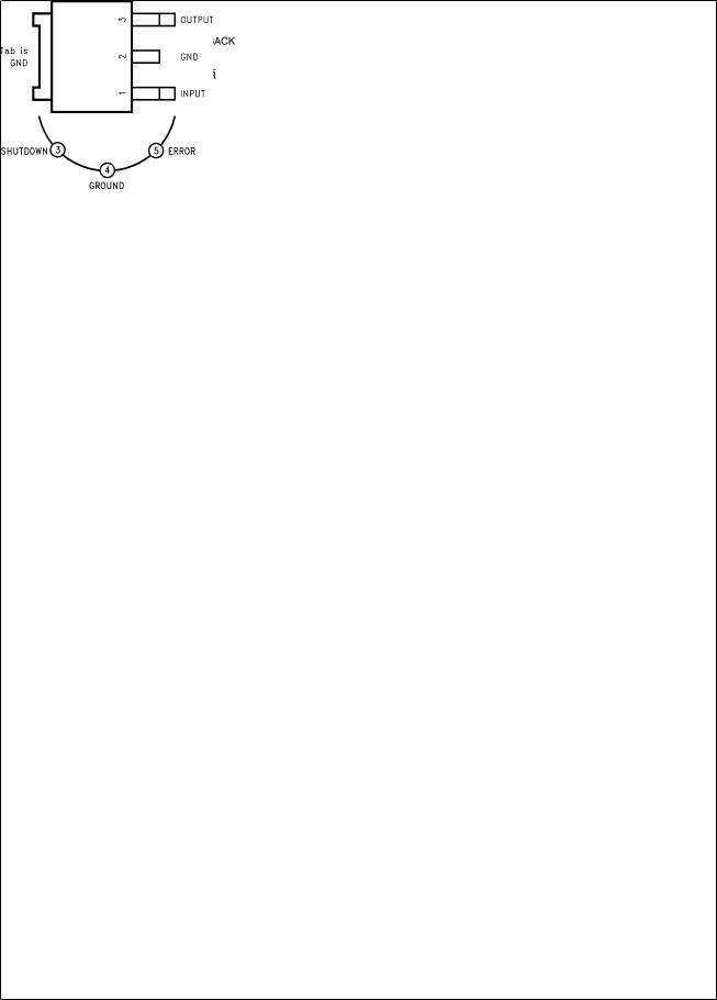
Connection Diagrams
TO-92 Plastic Package (Z)
DS008546-2
Bottom View
Metal Can Package (H)
DS008546-19
Top View
TO-252 (D-Pak)
DS008546-70
Front View
Dual-In-Line Packages (N, J)
Surface-Mount Package (M, MM)
DS008546-26
Top View
10-Lead Ceramic Surface-Mount Package (WG)
DS008546-64
Top View
www.national.com |
2 |

Ordering Information
Package |
|
Output Voltage |
|
|
Temperature |
|
|
|
|
|
|
|
3.0V |
3.3V |
5.0V |
|
(ÊC) |
|
|
|
|
|
|
TO-92 (Z) |
LP2950ACZ-3.0 |
LP2950ACZ-3.3 |
LP2950ACZ-5.0 |
−40 |
< TJ < 125 |
|
LP2950CZ-3.0 |
LP2950CZ-3.3 |
LP2950CZ-5.0 |
|
|
|
|
|
|
|
|
TO-252 (D-Pak) |
|
|
LP2950CDT-5.0 |
−40 |
< TJ < 125 |
N (N-08E) |
LP2951ACN-3.0 |
LP2951ACN-3.3 |
LP2951ACN |
−40 |
< TJ < 125 |
|
LP2951CN-3.0 |
LP2951CN-3.3 |
LP2951CN |
|
|
|
|
|
|
|
|
M (M08A) |
LP2951ACM-3.0 |
LP2951ACM-3.3 |
LP2951ACM |
−40 < TJ < 125 |
|
|
LP2951CM-3.0 |
LP2951CM-3.3 |
LP2951CM |
|
|
|
|
|
|
|
|
MM (MUA08A) |
LP2951ACMM-3.0 |
LP2951ACMM-3.3 |
LP2951ACMM |
−40 < TJ < 125 |
|
|
LP2951CMM-3.0 |
LP2951CMM-3.3 |
LP2951CMM |
|
|
|
|
|
|
|
|
J (J08A) |
|
|
LP2951ACJ |
−40 |
< TJ < 125 |
|
|
|
LP2951CJ |
|
|
|
|
|
LP2951J |
−55 |
< TJ < 150 |
|
|
|
LP2951J/883 |
|
|
|
|
|
5926-3870501MPA |
|
|
|
|
|
|
|
|
H (H08C) |
|
|
LP2951H/883 |
−55 |
< TJ < 150 |
|
|
|
5962-3870501MGA |
|
|
|
|
|
|
|
|
WG (WG10A) |
|
|
LP2951WG/883 |
−55 < TJ < 150 |
|
|
|
|
5962-3870501MXA |
|
|
|
|
|
|
|
|
Package Marking for MM Package:
Order Number |
Package Marking |
|
|
LP2951ACMM |
L0DA |
|
|
LP2951CMM |
L0DB |
|
|
LP2951ACMM-3.3 |
L0CA |
|
|
LP2951CMM-3.3 |
L0CB |
|
|
LP2951ACMM-3.0 |
L0BA |
|
|
LP2951CMM-3.0 |
L0BB |
|
|
LP2950/LP2951
3 |
www.national.com |

LP2950/LP2951
Absolute Maximum Ratings (Note 1)
If Military/Aerospace specified devices are required, please contact the National Semiconductor Sales Office/ Distributors for availability and specifications.
Input Supply Voltage |
−0.3 to +30V |
SHUTDOWN Input Voltage, |
|
Error Comparator Output |
|
Voltage, (Note 9) |
|
FEEDBACK Input Voltage |
−1.5 to +30V |
(Note 9) (Note 10) |
|
Power Dissipation |
Internally Limited |
Junction Temperature (TJ) |
+150ÊC |
Ambient Storage Temperature |
−65Ê to +150ÊC |
Soldering Dwell Time, Temperature |
|
Wave |
4 seconds, 260ÊC |
Infrared |
10 seconds, 240ÊC |
Vapor Phase |
75 seconds, 219ÊC |
ESD |
TBD |
Operating Ratings (Note 1)
Maximum Input Supply Voltage |
30V |
Junction Temperature Range |
|
(TJ) (Note 8) |
|
LP2951 |
−55Ê to +150ÊC |
LP2950AC-XX, LP2950C-XX, |
|
LP2951AC-XX, LP2951C-XX |
−40Ê to +125ÊC |
Electrical Characteristics (Note 2)
|
|
|
|
LP2951 |
|
LP2950AC-XX |
|
LP2950C-XX |
|
||
|
|
Conditions |
|
|
|
LP2951AC-XX |
|
LP2951C-XX |
|
||
|
|
|
|
|
|
|
|
|
|
|
|
Parameter |
|
|
Tested |
|
Tested |
Design |
|
Tested |
Design |
Units |
|
|
(Note 2) |
|
|
|
|||||||
|
|
Typ |
Limit |
Typ |
Limit |
Limit |
Typ |
Limit |
Limit |
|
|
|
|
|
|
||||||||
|
|
|
|
(Notes 3, 16) |
|
(Note 3) |
(Note 4) |
|
(Note 3) |
(Note 4) |
|
|
|
|
|
|
|
|
|
|
|
|
|
3V VERSIONS (Note 17) |
|
|
|
|
|
|
|
|
|
|
|
|
|
|
|
|
|
|
|
|
|
|
|
Output Voltage |
|
TJ = 25ÊC |
3.0 |
3.015 |
3.0 |
3.015 |
|
3.0 |
3.030 |
|
V max |
|
|
|
|
2.985 |
|
2.985 |
|
|
2.970 |
|
V min |
|
|
|
|
|
|
|
|
|
|
|
|
|
|
−25ÊC ≤ TJ ≤ 85ÊC |
3.0 |
|
3.0 |
|
3.030 |
3.0 |
|
3.045 |
V max |
|
|
|
|
|
|
|
2.970 |
|
|
2.955 |
V min |
|
|
|
|
|
|
|
|
|
|
|
|
|
|
Full Operating |
3.0 |
3.036 |
3.0 |
|
3.036 |
3.0 |
|
3.060 |
V max |
|
|
Temperature Range |
|
2.964 |
|
|
2.964 |
|
|
2.940 |
V min |
|
|
|
|
|
|
|
|
|
|
|
|
Output Voltage |
|
100 µA ≤ IL ≤ 100 mA |
3.0 |
3.045 |
3.0 |
|
3.042 |
3.0 |
|
3.072 |
V max |
|
|
TJ ≤ TJMAX |
|
2.955 |
|
|
2.958 |
|
|
2.928 |
V min |
3.3V VERSIONS (Note 17) |
|
|
|
|
|
|
|
|
|
|
|
|
|
|
|
|
|
|
|
|
|
|
|
Output Voltage |
|
TJ = 25ÊC |
3.3 |
3.317 |
3.3 |
3.317 |
|
3.3 |
3.333 |
|
V max |
|
|
|
|
3.284 |
|
3.284 |
|
|
3.267 |
|
V min |
|
|
|
|
|
|
|
|
|
|
|
|
|
|
−25ÊC ≤ TJ ≤ 85ÊC |
3.3 |
|
3.3 |
|
3.333 |
3.3 |
|
3.350 |
V max |
|
|
|
|
|
|
|
3.267 |
|
|
3.251 |
V min |
|
|
|
|
|
|
|
|
|
|
|
|
|
|
Full Operating |
3.3 |
3.340 |
3.3 |
|
3.340 |
3.3 |
|
3.366 |
V max |
|
|
Temperature Range |
|
3.260 |
|
|
3.260 |
|
|
3.234 |
V min |
|
|
|
|
|
|
|
|
|
|
|
|
Output Voltage |
|
100 µA ≤ IL ≤ 100 mA |
3.3 |
3.350 |
3.3 |
|
3.346 |
3.3 |
|
3.379 |
V max |
|
|
TJ ≤ TJMAX |
|
3.251 |
|
|
3.254 |
|
|
3.221 |
V min |
5V VERSIONS (Note 17) |
|
|
|
|
|
|
|
|
|
|
|
|
|
|
|
|
|
|
|
|
|
|
|
Output Voltage |
|
TJ = 25ÊC |
5.0 |
5.025 |
5.0 |
5.025 |
|
5.0 |
5.05 |
|
V max |
|
|
|
|
4.975 |
|
4.975 |
|
|
4.95 |
|
V min |
|
|
|
|
|
|
|
|
|
|
|
|
|
|
−25ÊC ≤ TJ ≤ 85ÊC |
5.0 |
|
5.0 |
|
5.05 |
5.0 |
|
5.075 |
V max |
|
|
|
|
|
|
|
4.95 |
|
|
4.925 |
V min |
|
|
|
|
|
|
|
|
|
|
|
|
|
|
Full Operating |
5.0 |
5.06 |
5.0 |
|
5.06 |
5.0 |
|
5.1 |
V max |
|
|
Temperature Range |
|
4.94 |
|
|
4.94 |
|
|
4.9 |
V min |
|
|
|
|
|
|
|
|
|
|
|
|
Output Voltage |
|
100 µA ≤ IL ≤ 100 mA |
5.0 |
5.075 |
5.0 |
|
5.075 |
5.0 |
|
5.12 |
V max |
|
|
TJ ≤ TJMAX |
|
4.925 |
|
|
4.925 |
|
|
4.88 |
V min |
ALL VOLTAGE OPTIONS |
|
|
|
|
|
|
|
|
|
|
|
|
|
|
|
|
|
|
|
|
|
|
|
Output Voltage |
|
(Note 12) |
20 |
120 |
20 |
|
100 |
50 |
|
150 |
ppm/ÊC |
Temperature Coefficient |
|
|
|
|
|
|
|
|
|
|
|
|
|
|
|
|
|
|
|
|
|
|
|
Line Regulation |
|
(VONOM + 1)V ≤ Vin ≤ 30V |
0.03 |
0.1 |
0.03 |
0.1 |
|
0.04 |
0.2 |
|
% max |
(Note 14) |
|
(Note 15) |
|
0.5 |
|
|
0.2 |
|
|
0.4 |
% max |
|
|
|
|
|
|
|
|
||||
|
|
|
|
|
|
|
|
|
|
|
|
Load Regulation |
|
100 µA ≤ IL ≤ 100 mA |
0.04 |
0.1 |
0.04 |
0.1 |
|
0.1 |
0.2 |
|
% max |
(Note 14) |
|
|
|
0.3 |
|
|
0.2 |
|
|
0.3 |
% max |
|
|
|
|
|
|
|
|
||||
|
|
|
|
|
|
|
|
|
|
|
|
www.national.com |
4 |

Electrical Characteristics (Note 2) |
(Continued) |
|
|
|
|
|
|
|
||||
|
|
|
|
|
|
|
|
|
|
|
|
|
|
|
|
|
|
LP2951 |
|
LP2950AC-XX |
|
LP2950C-XX |
|
||
|
|
Conditions |
|
|
|
|
LP2951AC-XX |
|
LP2951C-XX |
|
||
|
|
|
|
|
|
|
|
|
|
|
|
|
Parameter |
|
|
|
Tested |
|
Tested |
Design |
|
Tested |
Design |
Units |
|
|
(Note 2) |
|
|
|
|
|||||||
|
|
Typ |
|
Limit |
Typ |
Limit |
Limit |
Typ |
Limit |
Limit |
|
|
|
|
|
|
|
||||||||
|
|
|
|
|
(Notes 3, 16) |
|
(Note 3) |
(Note 4) |
|
(Note 3) |
(Note 4) |
|
|
|
|
|
|
|
|
|
|
|
|
|
|
ALL VOLTAGE OPTIONS |
|
|
|
|
|
|
|
|
|
|
|
|
|
|
|
|
|
|
|
|
|
|
|
|
|
Dropout Voltage |
|
IL = 100 µA |
|
|
80 |
|
80 |
|
|
80 |
|
mV max |
(Note 5) |
|
|
50 |
|
150 |
50 |
|
150 |
50 |
|
150 |
mV max |
|
|
|
|
|
|
|||||||
|
|
|
|
|
|
|
|
|
|
|
|
|
|
|
IL = 100 mA |
|
|
450 |
|
450 |
|
|
450 |
|
mV max |
|
|
|
380 |
|
600 |
380 |
|
600 |
380 |
|
600 |
mV max |
|
|
|
|
|
|
|
|
|
|
|
|
|
Ground |
|
IL = 100 µA |
75 |
|
120 |
75 |
120 |
|
75 |
120 |
|
µA max |
Current |
|
|
|
|
140 |
|
|
140 |
|
|
140 |
µA max |
|
|
|
|
|
|
|
|
|
|
|
|
|
|
|
IL = 100 mA |
8 |
|
12 |
8 |
12 |
|
8 |
12 |
|
mA max |
|
|
|
|
|
14 |
|
|
14 |
|
|
14 |
mA max |
|
|
|
|
|
|
|
|
|
|
|
|
|
Dropout |
|
Vin = (VONOM − 0.5)V |
110 |
|
170 |
110 |
170 |
|
110 |
170 |
|
µA max |
Ground Current |
|
IL = 100 µA |
|
|
200 |
|
|
200 |
|
|
200 |
µA max |
Current Limit |
|
Vout = 0 |
160 |
|
200 |
160 |
200 |
|
160 |
200 |
|
mA max |
|
|
|
|
|
220 |
|
|
220 |
|
|
220 |
mA max |
|
|
|
|
|
|
|
|
|
|
|
|
|
Thermal Regulation |
|
(Note 13) |
0.05 |
|
0.2 |
0.05 |
0.2 |
|
0.05 |
0.2 |
|
%/W max |
|
|
|
|
|
|
|
|
|
|
|
|
|
Output Noise, |
|
CL = 1 µF (5V Only) |
430 |
|
|
430 |
|
|
430 |
|
|
µV rms |
10 Hz to 100 kHz |
|
CL = 200 µF |
160 |
|
|
160 |
|
|
160 |
|
|
µV rms |
|
|
CL = 3.3 µF |
|
|
|
|
|
|
|
|
|
|
|
|
(Bypass = 0.01 µF |
100 |
|
|
100 |
|
|
100 |
|
|
µV rms |
|
|
Pins 7 to 1 (LP2951)) |
|
|
|
|
|
|
|
|
|
|
|
|
|
|
|
|
|
|
|
|
|
|
|
8-PIN VERSIONS ONLY |
|
|
|
LP2951 |
|
LP2951AC-XX |
|
LP2951C-XX |
|
|||
|
|
|
|
|
|
|
|
|
|
|
|
|
Reference |
|
|
1.235 |
|
1.25 |
1.235 |
1.25 |
|
1.235 |
1.26 |
|
V max |
Voltage |
|
|
|
|
1.26 |
|
|
1.26 |
|
|
1.27 |
V max |
|
|
|
|
|
1.22 |
|
1.22 |
|
|
1.21 |
|
V min |
|
|
|
|
|
1.2 |
|
|
1.2 |
|
|
1.2 |
V min |
|
|
|
|
|
|
|
|
|
|
|
|
|
Reference |
|
(Note 7) |
|
|
1.27 |
|
|
1.27 |
|
|
1.285 |
V max |
Voltage |
|
|
|
|
1.19 |
|
|
1.19 |
|
|
1.185 |
V min |
|
|
|
|
|
|
|
|
|
|
|
|
|
Feedback Pin |
|
|
20 |
|
40 |
20 |
40 |
|
20 |
40 |
|
nA max |
Bias Current |
|
|
|
|
60 |
|
|
60 |
|
|
60 |
nA max |
|
|
|
|
|
|
|
|
|
|
|
|
|
Reference Voltage |
|
(Note 12) |
20 |
|
|
20 |
|
|
50 |
|
|
ppm/ÊC |
Temperature Coefficient |
|
|
|
|
|
|
|
|
|
|
|
|
|
|
|
|
|
|
|
|
|
|
|
|
|
Feedback Pin Bias |
|
|
0.1 |
|
|
0.1 |
|
|
0.1 |
|
|
nA/ÊC |
Current Temperature |
|
|
|
|
|
|
|
|
|
|
|
|
Coefficient |
|
|
|
|
|
|
|
|
|
|
|
|
|
|
|
|
|
|
|
|
|
|
|
|
|
Error Comparator |
|
|
|
|
|
|
|
|
|
|
|
|
|
|
|
|
|
|
|
|
|
|
|
|
|
Output Leakage |
|
VOH = 30V |
0.01 |
|
1 |
0.01 |
1 |
|
0.01 |
1 |
|
µA max |
Current |
|
|
|
|
2 |
|
|
2 |
|
|
2 |
µA max |
|
|
|
|
|
|
|
|
|
|
|
|
|
Output Low |
|
Vin = (VONOM − 0.5)V |
150 |
|
250 |
150 |
250 |
|
150 |
250 |
|
mV max |
Voltage |
|
IOL = 400 µA |
|
|
400 |
|
|
400 |
|
|
400 |
mV max |
Upper Threshold |
|
(Note 6) |
60 |
|
40 |
60 |
40 |
|
60 |
40 |
|
mV min |
Voltage |
|
|
|
|
25 |
|
|
25 |
|
|
25 |
mV min |
|
|
|
|
|
|
|
|
|
|
|
|
|
Lower Threshold |
|
(Note 6) |
75 |
|
95 |
75 |
95 |
|
75 |
95 |
|
mV max |
Voltage |
|
|
|
|
140 |
|
|
140 |
|
|
140 |
mV max |
|
|
|
|
|
|
|
|
|
|
|
|
|
Hysteresis |
|
(Note 6) |
15 |
|
|
15 |
|
|
15 |
|
|
mV |
|
|
|
|
|
|
|
|
|
|
|
|
|
Shutdown Input |
|
|
|
|
|
|
|
|
|
|
|
|
|
|
|
|
|
|
|
|
|
|
|
|
|
Input |
|
|
1.3 |
|
|
1.3 |
|
|
1.3 |
|
|
V |
Logic |
|
Low (Regulator ON) |
|
|
0.6 |
|
|
0.7 |
|
|
0.7 |
V max |
Voltage |
|
High (Regulator OFF) |
|
|
2.0 |
|
|
2.0 |
|
|
2.0 |
V min |
|
|
|
|
|
|
|
|
|
|
|
|
|
LP2950/LP2951
5 |
www.national.com |
LP2950/LP2951
Electrical Characteristics (Note 2) (Continued)
|
|
|
LP2951 |
|
LP2950AC-XX |
|
LP2950C-XX |
|
||
|
Conditions |
|
|
|
LP2951AC-XX |
|
LP2951C-XX |
|
||
|
|
|
|
|
|
|
|
|
|
|
Parameter |
|
Tested |
|
Tested |
Design |
|
Tested |
Design |
Units |
|
(Note 2) |
|
|
|
|||||||
|
Typ |
Limit |
Typ |
Limit |
Limit |
Typ |
Limit |
Limit |
|
|
|
|
|
||||||||
|
|
|
(Notes 3, 16) |
|
(Note 3) |
(Note 4) |
|
(Note 3) |
(Note 4) |
|
|
|
|
|
|
|
|
|
|
|
|
Shutdown Input |
|
|
|
|
|
|
|
|
|
|
|
|
|
|
|
|
|
|
|
|
|
Shutdown Pin Input |
Vshutdown = 2.4V |
30 |
50 |
30 |
50 |
|
30 |
50 |
|
µA max |
Current |
|
|
100 |
|
|
100 |
|
|
100 |
µA max |
|
|
|
|
|
|
|
||||
|
|
|
|
|
|
|
|
|
|
|
|
Vshutdown = 30V |
450 |
600 |
450 |
600 |
|
450 |
600 |
|
µA max |
|
|
|
750 |
|
|
750 |
|
|
750 |
µA max |
|
|
|
|
|
|
|
|
|
|
|
Regulator Output |
(Note 11) |
3 |
10 |
3 |
10 |
|
3 |
10 |
|
µA max |
Current in Shutdown |
|
|
20 |
|
|
20 |
|
|
20 |
µA max |
|
|
|
|
|
|
|
||||
|
|
|
|
|
|
|
|
|
|
|
Note 1: Absolute Maximum Ratings are limits beyond which damage to the device may occur. Operating Ratings are conditions under which operation of the device is guaranteed. Operating Ratings do not imply guaranteed performance limits. For guaranteed performance limits and associated test conditions, see the Electrical Characteristics tables.
Note 2: Unless otherwise specified all limits guaranteed for VIN = (VONOM + 1)V, IL = 100 µA and CL = 1 µF for 5V versions and 2.2 µF for 3V and 3.3V versions. Limits appearing in boldface type apply over the entire junction temperature range for operation. Limits appearing in normal type apply for TA = TJ = 25ÊC. Additional
conditions for the 8-pin versions are FEEDBACK tied to VTAP, OUTPUT tied to SENSE, and VSHUTDOWN £ 0.8V. Note 3: Guaranteed and 100% production tested.
Note 4: Guaranteed but not 100% production tested. These limits are not used to calculate outgoing AQL levels.
Note 5: Dropout Voltage is defined as the input to output differential at which the output voltage drops 100 mV below its nominal value measured at 1V differential. At very low values of programmed output voltage, the minimum input supply voltage of 2V (2.3V over temperature) must be taken into account.
Note 6: Comparator thresholds are expressed in terms of a voltage differential at the Feedback terminal below the nominal reference voltage measured at Vin = (VONOM + 1)V. To express these thresholds in terms of output voltage change, multiply by the error amplifier gain = Vout/Vref = (R1 + R2)/R2.
For example, at a programmed output voltage of 5V, the Error output is guaranteed to go low when the output drops by 95 mV x 5V/1.235V = 384 mV. Thresholds remain constant as a percent of Vout as Vout is varied, with the dropout warning occurring at typically 5% below nominal, 7.5% guaranteed.
Note 7: Vref £ Vout £ (Vin − 1V), 2.3V £ Vin £ 30V, 100 µA £ IL £ 100 mA, TJ £ TJMAX.
Note 8: The junction-to-ambient thermal resistances are as follows: 180ÊC/W and 160ÊC/W for the TO-92 package with 0.40 inch and 0.25 inch leads to the printed circuit board (PCB) respectively, 105ÊC/W for the molded plastic DIP (N), 130ÊC/W for the ceramic DIP (J), 160ÊC/W for the molded plastic SOP (M), 200Ê C/W for the molded plastic MSOP (MM), and 160ÊC/W for the metal can package (H). The above thermal resistances for the N, J, M, and MM packages apply when the package is soldered directly to the PCB. Junction-to-case thermal resistance for the H package is 20ÊC/W. Junction-to-case thermal resistance for the TO-252 package is 5.4ÊC/W.
Note 9: May exceed input supply voltage.
Note 10: When used in dual-supply systems where the output terminal sees loads returned to a negative supply, the output voltage should be diode-clamped to ground.
Note 11: Vshutdown ³ 2V, Vin £ 30V, Vout = 0, Feedback pin tied to VTAP.
Note 12: Output or reference voltage temperature coefficient is defined as the worst case voltage change divided by the total temperature range.
Note 13: Thermal regulation is defined as the change in output voltage at a time T after a change in power dissipation is applied, excluding load or line regulation effects. Specifications are for a 50 mA load pulse at VIN = 30V (1.25W pulse) for T = 10 ms.
Note 14: Regulation is measured at constant junction temperature, using pulse testing with a low duty cycle. Changes in output voltage due to heating effects are covered under the specification for thermal regulation.
Note 15: Line regulation for the LP2951 is tested at 150ÊC for IL = 1 mA. For IL = 100 µA and TJ = 125ÊC, line regulation is guaranteed by design to 0.2%. See Typical Performance Characteristics for line regulation versus temperature and load current.
Note 16: A Military RETS specification is available on request. At time of printing, the LP2951 RETS specification complied with the boldface limits in this column. The LP2951H, WG, or J may also be procured as Standard Military Drawing Spec #5962-3870501MGA, MXA, or MPA.
Note 17: All LP2950 devices have the nominal output voltage coded as the last two digits of the part number. In the LP2951 products, the 3.0V and 3.3V versions are designated by the last two digits, but the 5V version is denoted with no code at this location of the part number (refer to ordering information table).
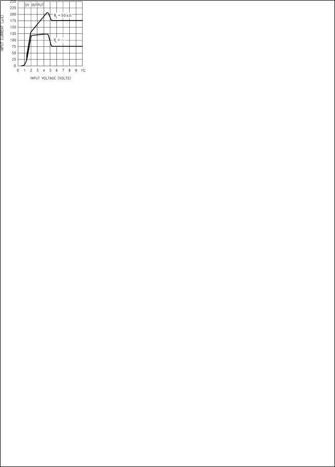
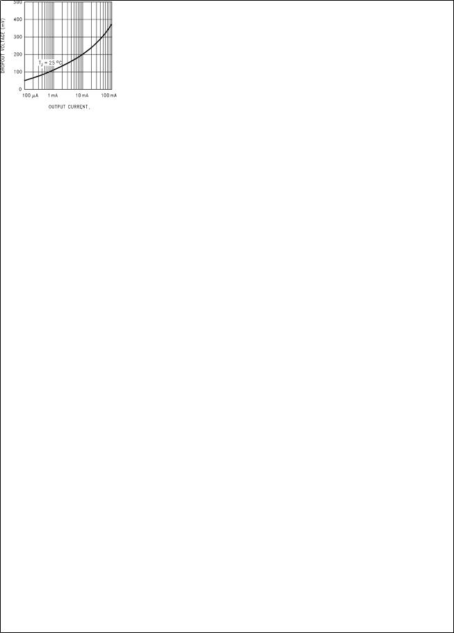
Typical Performance Characteristics
Quiescent Current |
Dropout Characteristics |
Input Current |
DS008546-27 |
DS008546-28 |
DS008546-29 |
www.national.com |
6 |
Typical Performance Characteristics (Continued)
Input Current |
Output Voltage vs. |
Quiescent Current |
|
Temperature of 3 |
|
|
Representative Units |
|
DS008546-30 |
DS008546-32 |
|
|
|
DS008546-31 |
Quiescent Current Quiescent Current Quiescent Current
DS008546-33 DS008546-34 DS008546-35
Short Circuit Current Dropout Voltage Dropout Voltage
DS008546-36 |
DS008546-37 |
DS008546-38 |
LP2950/LP2951
7 |
www.national.com |
 Loading...