


NSC LMS8117AMPX-3.3, LMS8117AMP-ADJ, LMS8117AMP-1.8, LMS8117ADTX-ADJ, LMS8117ADTX-3.3 Datasheet
...July 2001
LMS8117A
1A Low-Dropout Linear Regulator
General Description
The LMS8117A is a series of low dropout voltage regulators with a dropout of 1.2V at 1A of load current. It has the same pin-out as National Semiconductor's industry standard LM317.
The LMS8117A is available in an adjustable version, which can set the output voltage from 1.25V to 13.8V with only two external resistors. In addition, it is also available in two fixed voltages, 1.8V and 3.3V.
The LMS8117A offers current limiting and thermal shutdown. Its circuit includes a zener trimmed bandgap reference to assure output voltage accuracy to within ±1%.
The LMS8117A series is available in SOT-223 and TO-252 D-PAK packages. A minimum of 10µF tantalum capacitor is required at the output to improve the transient response and stability.
Features
nAvailable in 1.8V, 3.3V, and Adjustable Versions
nSpace Saving SOT-223 and TO-252 Packages
nCurrent Limiting and Thermal Protection
n Output Current |
1A |
|
n Temperature Range |
0ÊC to 125ÊC |
|
n |
Line Regulation |
0.2% (Max) |
n |
Load Regulation |
0.4% (Max) |
Applications
nPost Regulator for Switching DC/DC Converter
nHigh Efficiency Linear Regulators
nBattery Charger
nBattery Powered Instrumentation
Typical Application
Fixed Output Regulator
DS101196-28
Regulator Linear Dropout-Low 1A LMS8117A
© 2001 National Semiconductor Corporation |
DS101196 |
www.national.com |
LMS8117A
Ordering Information
|
Temperature Range |
|
|
NSC |
|
Package |
(TJ) |
Packaging Marking |
Transport Media |
||
Drawing |
|||||
|
0ÊC to +125ÊC |
|
|
||
|
|
|
|
||
|
|
|
|
|
|
3-lead |
LMS8117AMP-ADJ |
LS0A |
1k Tape and Reel |
MP04A |
|
SOT-223 |
|
|
|
|
|
LMS8117AMPX-ADJ |
LS0A |
2k Tape and Reel |
|
||
|
|
|
|
|
|
|
LMS8117AMP-1.8 |
LS00 |
1k Tape and Reel |
|
|
|
|
|
|
|
|
|
LMS8117AMPX-1.8 |
LS00 |
2k Tape and Reel |
|
|
|
|
|
|
|
|
|
LMS8117AMP-3.3 |
LS01 |
1k Tape and Reel |
|
|
|
|
|
|
|
|
|
LMS8117AMPX-3.3 |
LS01 |
2k Tape and Reel |
|
|
|
|
|
|
|
|
3-lead TO-252 |
LMS8117ADT-ADJ |
LMS8117ADT-ADJ |
Rails |
TD03B |
|
|
|
|
|
|
|
|
LMS8117ADTX-ADJ |
LMS8117ADT-ADJ |
2.5k Tape and Reel |
|
|
|
|
|
|
|
|
|
LMS8117ADT-1.8 |
LMS8117ADT-1.8 |
Rails |
|
|
|
|
|
|
|
|
|
LMS8117ADTX-1.8 |
LMS8117ADT-1.8 |
2.5k Tape and Reel |
|
|
|
|
|
|
|
|
|
LMS8117ADT-3.3 |
LMS8117ADT-3.3 |
Rails |
|
|
|
|
|
|
|
|
|
LMS8117ADTX-3.3 |
LMS8117ADT-3.3 |
2.5k Tape and Reel |
|
|
|
|
|
|
|
|
Connection Diagrams |
|
|
|
||
|
SOT-223 |
|
TO-252 |
|
|
DS101196-99
Top View
DS101196-38
Top View
www.national.com |
2 |

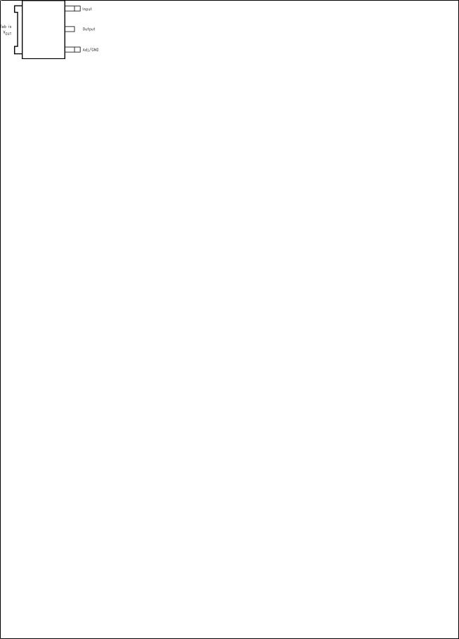
Block Diagram
LMS8117A
DS101196-1
3 |
www.national.com |

LMS8117A
Absolute Maximum Ratings (Note 1)
If Military/Aerospace specified devices are required, please contact the National Semiconductor Sales Office/ Distributors for availability and specifications.
Maximum Input Voltage (VIN to GND) |
|
|
LMS8117A-ADJ, LMS8117A-1.8, |
|
|
LMS8117A-3.3 |
20V |
|
Power Dissipation (Note 2) |
Internally Limited |
|
Junction Temperature (TJ) |
150ÊC |
|
(Note 2) |
||
|
||
Storage Temperature Range |
-65ÊC to 150ÊC |
Soldering Information |
|
Infrared (20 sec) |
235ÊC |
ESD Tolerance (Note 3) |
2000V |
Operating Ratings (Note 1)
Input Voltage (VIN to GND) |
|
LMS8117A-ADJ, LMS8117A-1.8, |
|
LMS8117A-3.3 |
15V |
Junction Temperature Range |
0ÊC to 125ÊC |
(TJ)(Note 2) |
|
Electrical Characteristics
Typicals and limits appearing in normal type apply for TJ = 25ÊC. Limits appearing in Boldface type apply over the entire junction temperature range for operation, 0ÊC to 125ÊC.
Symbol |
Parameter |
Conditions |
Min |
Typ |
Max |
Units |
|
(Note 5) |
(Note 4) |
(Note 5) |
|||||
|
|
|
|
||||
|
|
|
|
|
|
|
|
VREF |
Reference Voltage |
LMS8117A-ADJ |
|
|
|
|
|
|
|
IOUT = 10mA, VIN-VOUT = 2V, TJ = 25ÊC |
1.238 |
1.250 |
1.262 |
V |
|
|
|
10mA ≤ IOUT ≤ 1A, 1.4V ≤ VIN-VOUT ≤ |
1.225 |
1.250 |
1.270 |
V |
|
|
|
10V |
|
|
|
|
|
|
|
|
|
|
|
|
|
VOUT |
Output Voltage |
LMS8117A-1.8 |
|
|
|
|
|
|
|
IOUT = 10mA, VIN = 3.8V, TJ = 25ÊC |
1.782 |
1.800 |
1.818 |
V |
|
|
|
0 ≤ IOUT ≤ 1A, 3.2V ≤ VIN ≤ 10V |
1.746 |
1.800 |
1.854 |
V |
|
|
|
LMS8117A-3.3 |
|
|
|
|
|
|
|
IOUT = 10mA, VIN = 5V TJ = 25ÊC |
3.267 |
3.300 |
3.333 |
V |
|
|
|
0 ≤ IOUT ≤ 1A, 4.75V ≤ VIN ≤ 10V |
3.235 |
3.300 |
3.365 |
V |
|
VOUT |
Line Regulation |
LMS8117A-ADJ |
|
|
|
|
|
|
(Note 6) |
IOUT = 10mA, 1.5V ≤ VIN-VOUT ≤ 13.75V |
|
0.035 |
0.2 |
% |
|
|
|
LMS8117A-1.8 |
|
1 |
6 |
mV |
|
|
|
IOUT = 0mA, 3.2V ≤ VIN ≤ 10V |
|
|
|
|
|
|
|
LMS8117A-3.3 |
|
|
|
|
|
|
|
IOUT = 0mA, 4.75V ≤ VIN ≤ 15V |
|
1 |
6 |
mV |
|
VOUT |
Load Regulation |
LMS8117A-ADJ |
|
|
|
|
|
|
(Note 6) |
VIN-VOUT = 3V, 10mA ≤ IOUT ≤ 1A |
|
0.2 |
0.4 |
% |
|
|
|
LMS8117A-1.8 |
|
|
|
|
|
|
|
VIN = 3.2V, 0 ≤ IOUT ≤ 1A |
|
1 |
10 |
mV |
|
|
|
LMS8117A-3.3 |
|
|
|
|
|
|
|
VIN = 4.75V, 0 ≤ IOUT ≤ 1A |
|
1 |
10 |
mV |
|
VIN-V OUT |
Dropout Voltage |
IOUT = 100mA |
|
1.1 |
1.15 |
V |
|
|
(Note 7) |
IOUT = 500mA |
|
1.15 |
1.2 |
V |
|
|
|
IOUT = 1A |
|
1.2 |
1.25 |
V |
|
ILIMIT |
Current Limit |
VIN-VOUT = 5V, TJ = 25ÊC |
1.0 |
1.4 |
1.9 |
A |
|
|
Minimum Load |
LMS8117A-ADJ |
|
|
|
|
|
|
Current (Note 8) |
VIN = 15V |
|
1.7 |
5 |
mA |
|
|
Quiescent Current |
LMS8117A-1.8 |
|
5 |
10 |
mA |
|
|
|
VIN ≤ 15V |
|
|
|
|
|
|
|
LMS8117A-3.3 |
|
|
|
|
|
|
|
VIN ≤ 15V |
|
5 |
10 |
mA |
|
|
Thermal Regulation |
TA = 25ÊC, 30ms Pulse |
|
0.01 |
0.1 |
%/W |
|
|
Ripple Regulation |
fRIPPLE = 120Hz, VIN-VOUT = 3V |
60 |
75 |
|
dB |
|
|
|
VRIPPLE = 1VPP |
|
|
|
|
|
|
Adjust Pin Current |
|
|
60 |
120 |
µA |
|
|
|
|
|
|
|
|
|
|
Adjust Pin Current |
10mA ≤ IOUT ≤ 1A, |
|
|
|
|
|
|
Change |
1.4V ≤ VIN-VOUT ≤ 10V |
|
0.2 |
5 |
µA |
www.national.com |
4 |

Electrical Characteristics (Continued)
Typicals and limits appearing in normal type apply for TJ = 25ÊC. Limits appearing in Boldface type apply over the entire junction temperature range for operation, 0ÊC to 125ÊC.
Symbol |
Parameter |
Conditions |
Min |
Typ |
Max |
Units |
|
(Note 5) |
(Note 4) |
(Note 5) |
|||||
|
|
|
|
||||
|
|
|
|
|
|
|
|
|
Temperature Stability |
|
|
0.5 |
|
% |
|
|
|
|
|
|
|
|
|
|
Long Term Stability |
TA = 125ÊC, 1000Hrs |
|
0.3 |
|
% |
|
|
RMS Output Noise |
(% of VOUT), 10Hz ≤ f ≤ 10kHz |
|
0.003 |
|
% |
|
|
Thermal Resistance |
3-Lead SOT-223 |
|
15.0 |
|
ÊC/W |
|
|
Junction-to-Case |
3-Lead TO-252 |
|
10 |
|
ÊC/W |
|
|
|
|
|
|
|
|
|
|
Thermal Resistance |
3-Lead SOT-223 |
|
136 |
|
ÊC/W |
|
|
Junction-to-Ambient |
3-Lead TO-252 (Note 9) |
|
92 |
|
ÊC/W |
|
|
(No heat sink; |
|
|
|
|
|
|
|
No air flow) |
|
|
|
|
|
|
|
|
|
|
|
|
|
Note 1: Absolute Maximum Ratings indicate limits beyond which damage to the device may occur. Operating Ratings indicate conditions for which the device is intended to be functional, but specific performance is not guaranteed. For guaranteed specifications and the test conditions, see the Electrical Characteristics.
Note 2: The maximum power dissipation is a function of TJ(MAX) , θJA, and TA. The maximum allowable power dissipation at any ambient temperature is PD = (TJ(MAX)±TA)/θJA. All numbers apply for packages soldered directly into a PC board.
Note 3: For testing purposes, ESD was applied using human body model, 1.5kΩ in series with 100pF.
Note 4: Typical Values represent the most likely parametric norm.
Note 5: All limits are guaranteed by testing or statistical analysis.
Note 6: Load and line regulation are measured at constant junction room temperature.
Note 7: The dropout voltage is the input/output differential at which the circuit ceases to regulate against further reduction in input voltage. It is measured when the output voltage has dropped 100mV from the nominal value obtained at VIN = VOUT +1.5V.
Note 8: The minimum output current required to maintain regulation.
Note 9: Minimum pad size of 0.038in2
LMS8117A
5 |
www.national.com |
 Loading...