


NSC LM555J-883, LM555H-883, LM555H-MLS, LM555CMX, LM555CMMX Datasheet
...
February 2000
LM555
Timer
General Description
The LM555 is a highly stable device for generating accurate time delays or oscillation. Additional terminals are provided for triggering or resetting if desired. In the time delay mode of operation, the time is precisely controlled by one external resistor and capacitor. For astable operation as an oscillator, the free running frequency and duty cycle are accurately controlled with two external resistors and one capacitor. The circuit may be triggered and reset on falling waveforms, and the output circuit can source or sink up to 200mA or drive TTL circuits.
Features
nDirect replacement for SE555/NE555
nTiming from microseconds through hours
nOperates in both astable and monostable modes
nAdjustable duty cycle
nOutput can source or sink 200 mA
nOutput and supply TTL compatible
nTemperature stability better than 0.005% per ÊC
nNormally on and normally off output
nAvailable in 8-pin MSOP package
Applications
nPrecision timing
nPulse generation
nSequential timing
nTime delay generation
nPulse width modulation
nPulse position modulation
nLinear ramp generator
Schematic Diagram
DS007851-1
Timer LM555
© 2000 National Semiconductor Corporation |
DS007851 |
www.national.com |
LM555
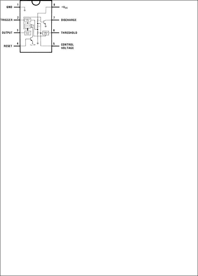
Connection Diagram
Dual-In-Line, Small Outline
and Molded Mini Small Outline Packages
|
|
|
DS007851-3 |
|
|
|
Top View |
|
|
Ordering Information |
|
|
|
|
|
|
|
|
|
Package |
Part Number |
Package Marking |
Media Transport |
NSC Drawing |
|
|
|
|
|
8-Pin SOIC |
LM555CM |
LM555CM |
Rails |
M08A |
|
|
|
|
|
|
LM555CMX |
LM555CM |
2.5k Units Tape and Reel |
|
|
|
|||
|
|
|
|
|
8-Pin MSOP |
LM555CMM |
Z55 |
1k Units Tape and Reel |
MUA08A |
|
|
|
|
|
|
LM555CMMX |
Z55 |
3.5k Units Tape and Reel |
|
|
|
|||
|
|
|
|
|
8-Pin MDIP |
LM555CN |
LM555CN |
Rails |
N08E |
|
|
|
|
|
www.national.com |
2 |

Absolute Maximum Ratings (Note 2)
If Military/Aerospace specified devices are required, please contact the National Semiconductor Sales Office/ Distributors for availability and specifications.
Supply Voltage |
+18V |
Power Dissipation (Note 3) |
|
LM555CM, LM555CN |
1180 mW |
LM555CMM |
613 mW |
Operating Temperature Ranges |
|
LM555C |
0ÊC to +70ÊC |
Storage Temperature Range |
−65ÊC to +150ÊC |
Soldering Information |
|
Dual-In-Line Package |
|
Soldering (10 Seconds) |
260ÊC |
Small Outline Packages |
|
(SOIC and MSOP) |
|
Vapor Phase (60 Seconds) |
215ÊC |
Infrared (15 Seconds) |
220ÊC |
See AN-450 ªSurface Mounting Methods and Their Effect on Product Reliabilityº for other methods of soldering surface mount devices.
Electrical Characteristics (Notes 1, 2)
(TA = 25ÊC, VCC = +5V to +15V, unless othewise specified)
Parameter |
Conditions |
|
Limits |
|
Units |
|
|
|
|
|
|
|
|
|
LM555C |
|
|
|
|
|
|
|
|
|
|
Min |
Typ |
Max |
|
|
|
|
|
|
|
Supply Voltage |
|
4.5 |
|
16 |
V |
|
|
|
|
|
|
Supply Current |
VCC = 5V, RL = ∞ |
|
3 |
6 |
|
|
VCC = 15V, RL = ∞ |
|
10 |
15 |
mA |
|
(Low State) (Note 4) |
|
|
|
|
|
|
|
|
|
|
Timing Error, Monostable |
|
|
|
|
|
Initial Accuracy |
|
|
1 |
|
% |
Drift with Temperature |
RA = 1k to 100kΩ, |
|
50 |
|
ppm/ÊC |
|
C = 0.1µF, (Note 5) |
|
|
|
|
Accuracy over Temperature |
|
|
1.5 |
|
% |
Drift with Supply |
|
|
0.1 |
|
%/V |
|
|
|
|
|
|
Timing Error, Astable |
|
|
|
|
|
Initial Accuracy |
|
|
2.25 |
|
% |
Drift with Temperature |
RA, RB = 1k to 100kΩ, |
|
150 |
|
ppm/ÊC |
|
C = 0.1µF, (Note 5) |
|
|
|
|
Accuracy over Temperature |
|
|
3.0 |
|
% |
Drift with Supply |
|
|
0.30 |
|
%/V |
|
|
|
|
|
|
Threshold Voltage |
|
|
0.667 |
|
x VCC |
Trigger Voltage |
VCC = 15V |
|
5 |
|
V |
|
VCC = 5V |
|
1.67 |
|
V |
Trigger Current |
|
|
0.5 |
0.9 |
µA |
|
|
|
|
|
|
Reset Voltage |
|
0.4 |
0.5 |
1 |
V |
|
|
|
|
|
|
Reset Current |
|
|
0.1 |
0.4 |
mA |
|
|
|
|
|
|
Threshold Current |
(Note 6) |
|
0.1 |
0.25 |
µA |
|
|
|
|
|
|
Control Voltage Level |
VCC = 15V |
9 |
10 |
11 |
V |
|
VCC = 5V |
2.6 |
3.33 |
4 |
|
|
|
||||
Pin 7 Leakage Output High |
|
|
1 |
100 |
nA |
|
|
|
|
|
|
Pin 7 Sat (Note 7) |
|
|
|
|
|
Output Low |
VCC = 15V, I7 = 15mA |
|
180 |
|
mV |
Output Low |
VCC = 4.5V, I7 = 4.5mA |
|
80 |
200 |
mV |
LM555
3 |
www.national.com |

LM555
Electrical Characteristics (Notes 1, 2) (Continued)
(TA = 25ÊC, VCC = +5V to +15V, unless othewise specified)
Parameter |
Conditions |
|
Limits |
|
Units |
|
|
|
|
|
|
|
|
|
LM555C |
|
|
|
|
|
|
|
|
|
|
Min |
Typ |
Max |
|
|
|
|
|
|
|
Output Voltage Drop (Low) |
VCC = 15V |
|
|
|
|
|
ISINK = 10mA |
|
0.1 |
0.25 |
V |
|
ISINK = 50mA |
|
0.4 |
0.75 |
V |
|
ISINK = 100mA |
|
2 |
2.5 |
V |
|
ISINK = 200mA |
|
2.5 |
|
V |
|
VCC = 5V |
|
|
|
|
|
ISINK = 8mA |
|
|
|
V |
|
ISINK = 5mA |
|
0.25 |
0.35 |
V |
Output Voltage Drop (High) |
ISOURCE = 200mA, VCC = 15V |
|
12.5 |
|
V |
|
ISOURCE = 100mA, VCC = 15V |
12.75 |
13.3 |
|
V |
|
VCC = 5V |
2.75 |
3.3 |
|
V |
Rise Time of Output |
|
|
100 |
|
ns |
|
|
|
|
|
|
Fall Time of Output |
|
|
100 |
|
ns |
|
|
|
|
|
|
Note 1: All voltages are measured with respect to the ground pin, unless otherwise specified.
Note 2: Absolute Maximum Ratings indicate limits beyond which damage to the device may occur. Operating Ratings indicate conditions for which the device is functional, but do not guarantee specific performance limits. Electrical Characteristics state DC and AC electrical specifications under particular test conditions which guarantee specific performance limits. This assumes that the device is within the Operating Ratings. Specifications are not guaranteed for parameters where no limit is given, however, the typical value is a good indication of device performance.
Note 3: For operating at elevated temperatures the device must be derated above 25ÊC based on a +150ÊC maximum junction temperature and a thermal resistance of 106ÊC/W (DIP), 170ÊC/W (S0-8), and 204ÊC/W (MSOP) junction to ambient.
Note 4: Supply current when output high typically 1 mA less at VCC = 5V. Note 5: Tested at VCC = 5V and VCC = 15V.
Note 6: This will determine the maximum value of RA + RB for 15V operation. The maximum total (RA + RB) is 20MΩ.
Note 7: No protection against excessive pin 7 current is necessary providing the package dissipation rating will not be exceeded.
Note 8: Refer to RETS555X drawing of military LM555H and LM555J versions for specifications.
www.national.com |
4 |
 Loading...