


LM7171MD8
NSC LM7171MD8, LM7171BIWMX, LM7171BIWM, LM7171BIN, LM7171BIM Datasheet
...
LM7171
Very High Speed, High Output Current, Voltage
Feedback Amplifier
General Description
The LM7171 is a high speed voltage feedback amplifier that
has the slewing characteristic of a current feedback ampli-
fier; yet it can be used inalltraditionalvoltage feedback am-
plifier configurations. The LM7171 is stable for gains as low
as +2 or −1. It provides a very high slew rate at 4100V/µs
and a wide unity-gain bandwidth of 200 MHz while consum-
ing only 6.5 mA of supply current. It is ideal for video and
high speed signal processing applications such as HDSL
and pulse amplifiers. With 100 mA output current, the
LM7171 can be used for video distribution, as a transformer
driver or as a laser diode driver.
Operation on
±
15V power supplies allows for large signal
swings and provides greater dynamic range and
signal-to-noise ratio. The LM7171 offers low SFDR and
THD, ideal for ADC/DAC systems. In addition, the LM7171 is
specified for
±
5V operation for portable applications.
The LM7171 is built on National’s advanced VIP
™
III (Verti-
cally integrated PNP) complementary bipolar process.
Features
(Typical Unless Otherwise Noted)
n Easy-To-Use Voltage Feedback Topology
n Very High Slew Rate: 4100V/µs
n Wide Unity-Gain Bandwidth: 200 MHz
n −3 dB Frequency
@
A
V
=
+2: 220 MHz
n Low Supply Current: 6.5 mA
n High Open Loop Gain: 85 dB
n High Output Current: 100 mA
n Differential Gain and Phase: 0.01
%
, 0.02˚
n Specified for
±
15V and
±
5V Operation
Applications
n HDSL and ADSL Drivers
n Multimedia Broadcast Systems
n Professional Video Cameras
n Video Amplifiers
n Copiers/Scanners/Fax
n HDTV Amplifiers
n Pulse Amplifiers and Peak Detectors
n CATV/Fiber Optics Signal Processing
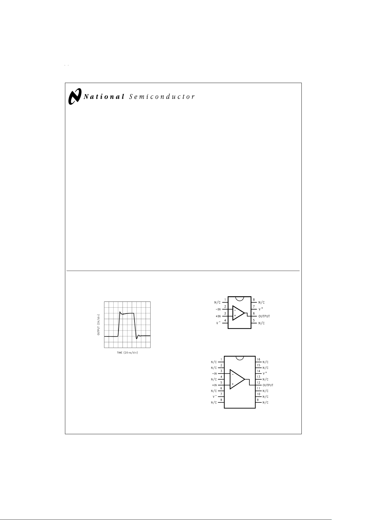
Typical Performance Connection Diagrams
VIP
™
is a trademark of National Semiconductor Corporation.
Large Signal Pulse Response
A
V
=
+2, V
S
=
±
15V
DS012385-1
8-Pin DIP/SO
DS012385-2
Top View
16-Pin Wide Body SO
DS012385-3
Top View
May 1999
LM7171 Very High Speed, High Output Current, Voltage Feedback Amplifier
© 1999 National Semiconductor Corporation DS012385 www.national.com
Ordering Information
Package Temperature Range Transport
Media
NSC
Drawing
Industrial Military
−40˚C to +85˚C −55˚C to +125˚C
8-Pin DIP LM7171AIN, LM7171BIN Rails N08E
8-Pin CDIP LM7171AMJ-QML
LM7171AMJ-QMLV
5962-95536 Rails J08A
10-Pin Ceramic
SOIC
LM7171AMWG-QML
LM7171AMWG-QMLV
5962-95536 Trays WG10A
8-Pin LM7171AIM, LM7171BIM Rails M08A
Small Outline LM7171AIMX, LM7171BIMX Tape and Reel
16-Pin LM7171AIWM, LM7171BIWM Rails M16B
Small Outline LM7171AWMX, LM7171BWMX Tape and Reel
www.national.com 2
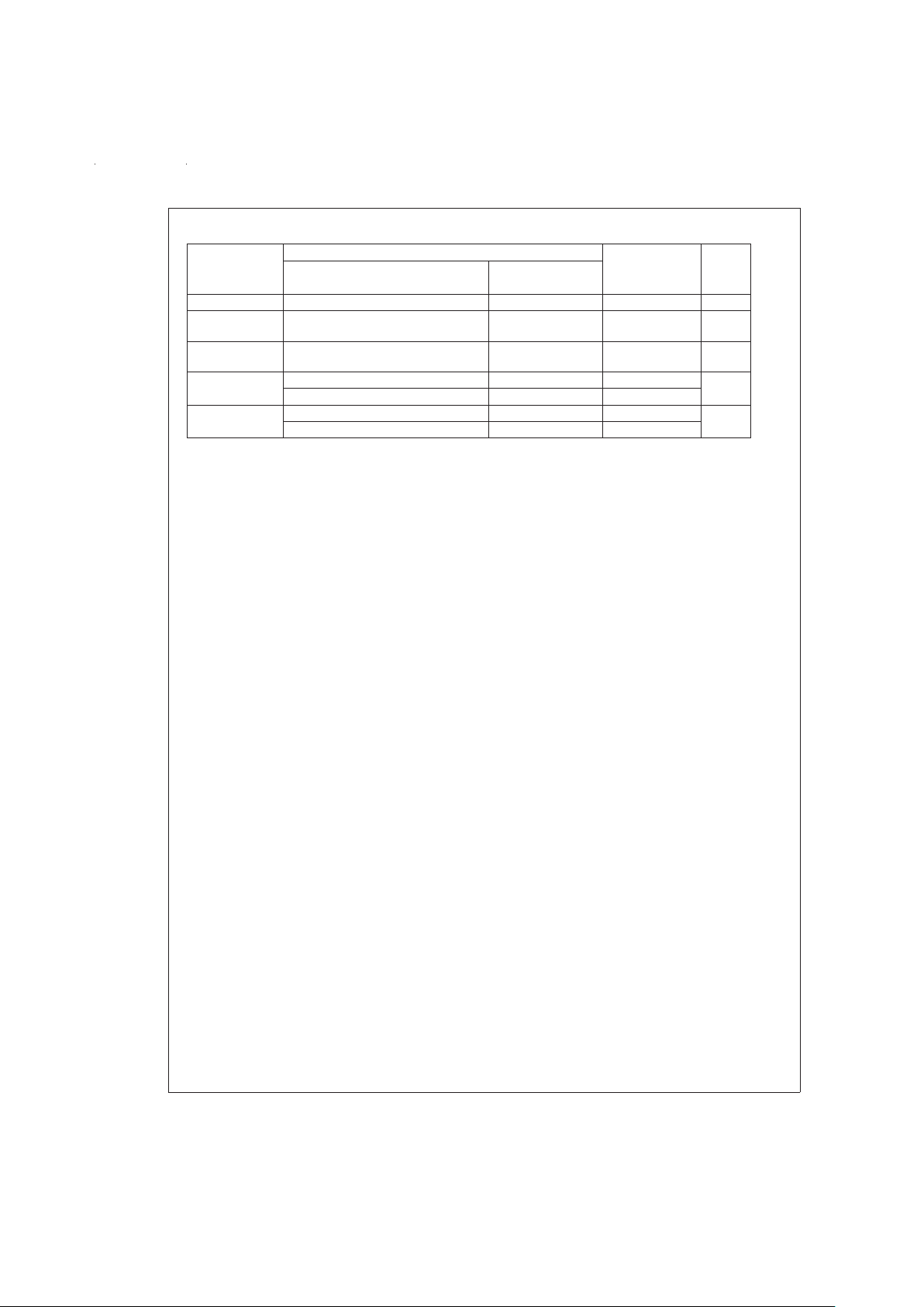
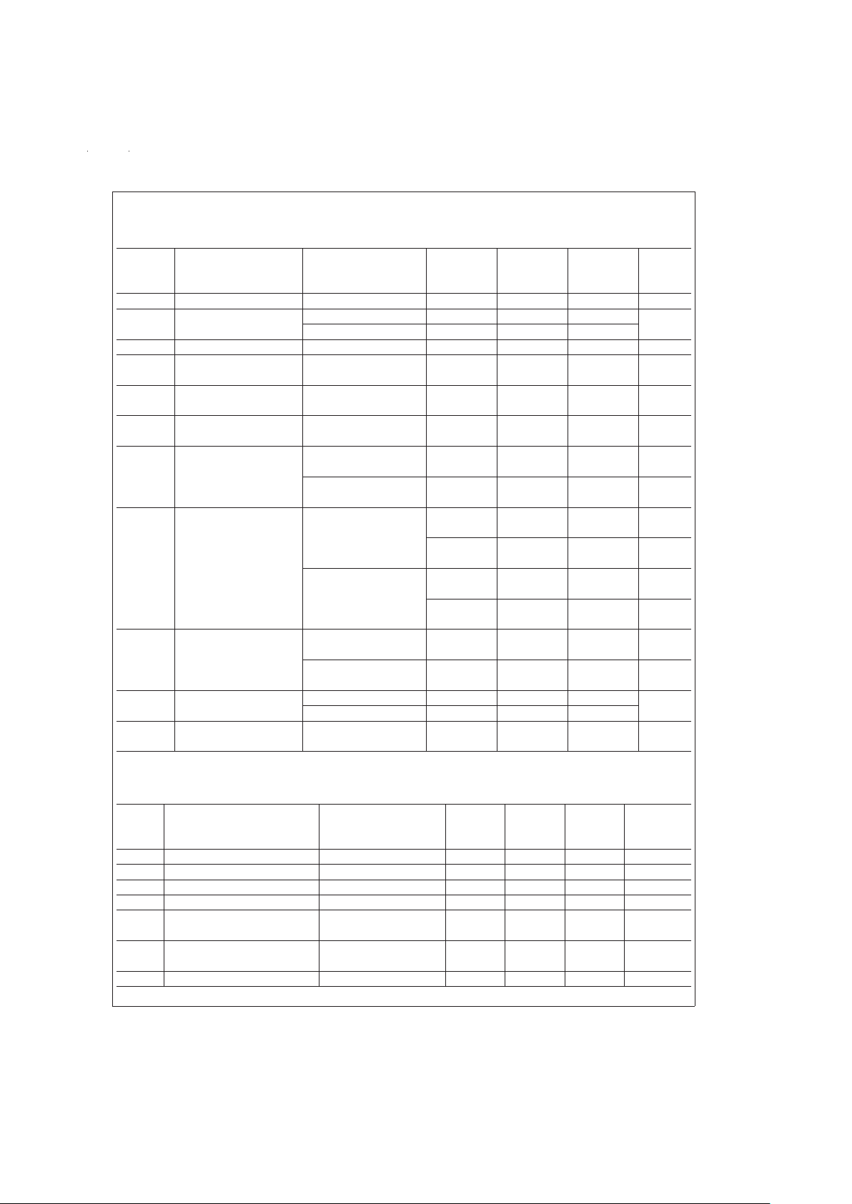
Absolute Maximum Ratings (Note 1)
If Military/Aerospace specified devices are required,
please contact the National Semiconductor Sales Office/
Distributors for availability and specifications.
ESD Tolerance (Note 2) 2.5 kV
Supply Voltage (V
+
–V
−
) 36V
Differential Input Voltage (Note 11)
±
10V
Output Short Circuit to Ground
(Note 3) Continuous
Storage Temperature Range −65˚C to +150˚C
Maximum Junction Temperature
(Note 4) 150˚C
Operating Ratings (Note 1)
Supply Voltage 5.5V ≤ V
S
≤ 36V
Junction Temperature Range
LM7171AI, LM7171BI −40˚C ≤ T
J
≤ +85˚C
Thermal Resistance (θ
JA
)
N Package, 8-Pin Molded DIP 108˚C/W
M Package, 8-Pin Surface Mount 172˚C/W
M Package, 16-Pin Surface Mount 95˚C/W
±
15V DC Electrical Characteristics
Unless otherwise specified, all limits guaranteed for T
J
=
25˚C, V
+
=
+15V, V
−
=
−15V, V
CM
=
0V, and R
L
=
1kΩ.Boldface
limits apply at the temperature extremes
Symbol Parameter Conditions Typ
(Note 5)
LM7171AI LM7171BI Units
Limit Limit
(Note 6) (Note 6)
V
OS
Input Offset Voltage 0.2 1 3 mV
47max
TC V
OS
Input Offset Voltage 35 µV/˚C
Average Drift
I
B
Input Bias Current 2.7 10 10 µA
12 12 max
I
OS
Input Offset Current 0.1 4 4 µA
66max
R
IN
Input Resistance Common Mode 40 MΩ
Differential Mode 3.3
R
O
Open Loop Output 15 Ω
Resistance
CMRR Common Mode V
CM
=
±
10V 105 85 75 dB
Rejection Ratio 80 70 min
PSRR Power Supply V
S
=
±
15V to
±
5V 90 85 75 dB
Rejection Ratio 80 70 min
V
CM
Input Common-Mode CMRR
>
60 dB
±
13.35 V
Voltage Range
A
V
Large Signal Voltage R
L
=
1kΩ 85 80 75 dB
Gain (Note 7) 75 70 min
R
L
=
100Ω 81 75 70 dB
70 66 min
V
O
Output Swing R
L
=
1kΩ 13.3 13 13 V
12.7 12.7 min
−13.2 −13 −13 V
−12.7 −12.7 max
R
L
=
100Ω 11.8 10.5 10.5 V
9.5 9.5 min
−10.5 −9.5 −9.5 V
−9 −9 max
Output Current Sourcing, R
L
=
100Ω 118 105 105 mA
(Open Loop) 95 95 min
(Note 8) Sinking, R
L
=
100Ω 105 95 95 mA
90 90 max
www.national.com3
±
15V DC Electrical Characteristics (Continued)
Unless otherwise specified, all limits guaranteed for T
J
=
25˚C, V
+
=
+15V, V
−
=
−15V, V
CM
=
0V, and R
L
=
1kΩ.Boldface
limits apply at the temperature extremes
Symbol Parameter Conditions Typ
(Note 5)
LM7171AI LM7171BI Units
Limit Limit
(Note 6) (Note 6)
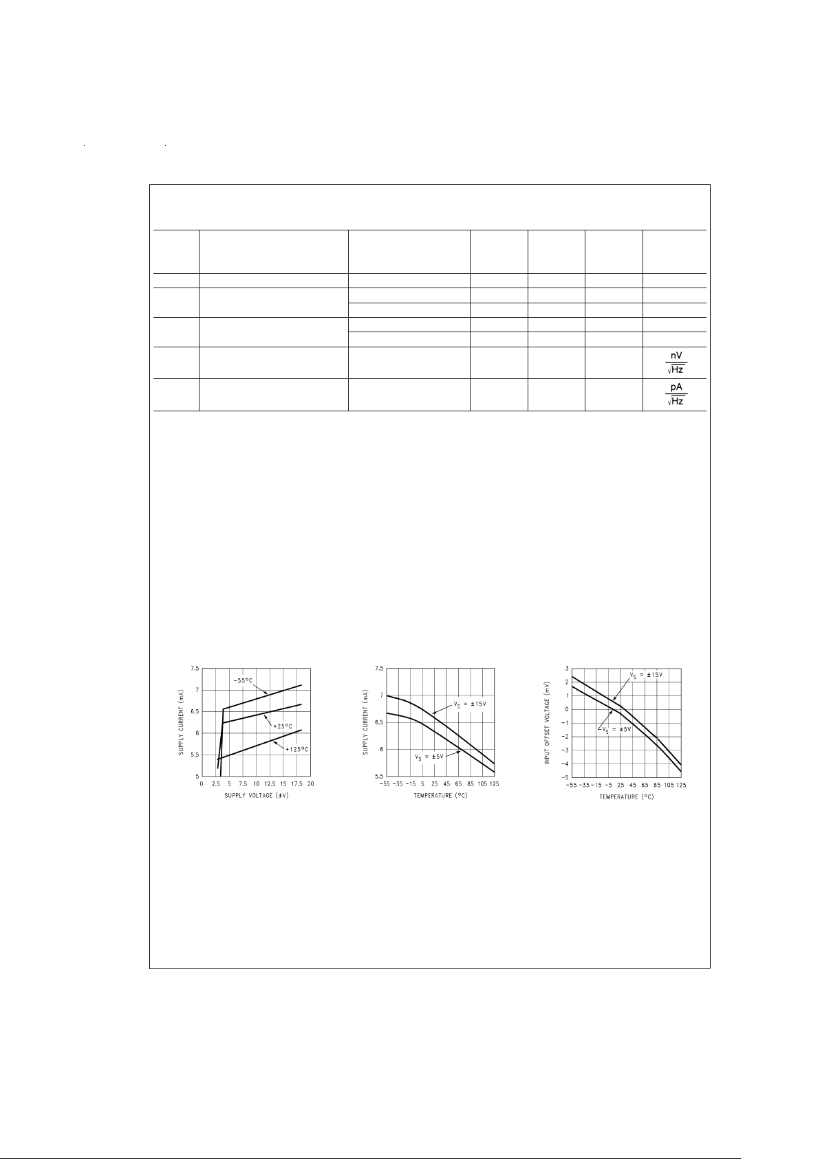
Output Current Sourcing, R
L
=
100Ω 100 mA
(in Linear Region) Sinking, R
L
=
100Ω 100
I
SC
Output Short Circuit Sourcing 140 mA
Current Sinking 135
I
S
Supply Current 6.5 8.5 8.5 mA
9.5 9.5 max
±
15V AC Electrical Characteristics
Unless otherwise specified, T
J
=
25˚C, V
+
=
+15V, V
−
=
−15V, V
CM
=
0V, and R
L
=
1kΩ.
Typ LM7171AI LM7171BI
Symbol Parameter Conditions (Note 5) Limit Limit Units
(Note 6) (Note 6)
SR Slew Rate (Note 9) A
V
=
+2, V
IN
=
13 V
PP
4100 V/µs
A
V
=
+2, V
IN
=
10 V
PP
3100
Unity-Gain Bandwidth 200 MHz
−3 dB Frequency A
V
=
+2 220 MHz
φ
m
Phase Margin 50 Deg
t
s
Settling Time (0.1
%
)A
V
=
−1, V
O
=
±
5V 42 ns
R
L
=
500Ω
t
p
Propagation Delay A
V
=
−2, V
IN
=
±
5V, 5 ns
R
L
=
500Ω
A
D
Differential Gain (Note 10) 0.01
%
φ
D
Differential Phase (Note 10) 0.02 Deg
Second Harmonic (Note 12) f
IN
=
10 kHz −110 dBc
f
IN
=
5 MHz −75 dBc
Third Harmonic (Note 12) f
IN
=
10 kHz −115 dBc
f
IN
=
5 MHz −55 dBc
e
n
Input-Referred f
=
10 kHz
14
Voltage Noise
i
n
Input-Referred f
=
10 kHz
1.5
Current Noise
±
5V DC Electrical Characteristics
Unless otherwise specified, all limits guaranteed for T
J
=
25˚C, V
+
=
+5V, V
−
=
−5V, V
CM
=
0V, and R
L
=
1kΩ.Boldface lim-
its apply at the temperature extremes
Typ LM7171AI LM7171BI
Symbol Parameter Conditions (Note 5) Limit Limit Units
(Note 6) (Note 6)
V
OS
Input Offset Voltage 0.3 1.5 3.5 mV
47max
TC V
OS
Input Offset Voltage 35 µV/˚C
Average Drift
I
B
Input Bias Current 3.3 10 10 µA
12 12 max
I
OS
Input Offset Current 0.1 4 4 µA
www.national.com 4
±
5V DC Electrical Characteristics (Continued)
Unless otherwise specified, all limits guaranteed for T
J
=
25˚C, V
+
=
+5V, V
−
=
−5V, V
CM
=
0V, and R
L
=
1kΩ.Boldface lim-
its apply at the temperature extremes
Typ LM7171AI LM7171BI
Symbol Parameter Conditions (Note 5) Limit Limit Units
(Note 6) (Note 6)
66max
R
IN
Input Resistance Common Mode 40 MΩ
Differential Mode 3.3
R
O
Output Resistance 15 Ω
CMRR Common Mode V
CM
=
±
2.5V 104 80 70 dB
Rejection Ratio 75 65 min
PSRR Power Supply V
S
=
±
15V to
±
5V 90 85 75 dB
Rejection Ratio 80 70 min
V
CM
Input Common-Mode CMRR
>
60 dB
±
3.2 V
Voltage Range
A
V
Large Signal Voltage R
L
=
1kΩ 78 75 70 dB
Gain (Note 7) 70 65 min
R
L
=
100Ω 76 72 68 dB
67 63 min
V
O
Output Swing R
L
=
1kΩ 3.4 3.2 3.2 V
33min
−3.4 −3.2 −3.2 V
−3 −3 max
R
L
=
100Ω 3.1 2.9 2.9 V
2.8 2.8 min
−3.0 −2.9 −2.9 V
−2.8 −2.8 max
Output Current Sourcing, R
L
=
100Ω 31 29 29 mA
(Open Loop) (Note 8) 28 28 min
Sinking, R
L
=
100Ω 30 29 29 mA
28 28 max
I
SC
Output Short Circuit Sourcing 135 mA
Current Sinking 100
I
S
Supply Current 6.2 8 8 mA
99max
±
5V AC Electrical Characteristics
Unless otherwise specified, T
J
=
25˚C, V
+
=
+5V, V
−
=
−5V, V
CM
=
0V, and R
L
=
1kΩ.
Typ LM7171AI LM7171BI
Symbol Parameter Conditions (Note 5) Limit Limit Units
(Note 6) (Note 6)
SR Slew Rate (Note 9) A
V
=
+2, V
IN
=
3.5 V
PP
950 V/µs
Unity-Gain Bandwidth 125 MHz
−3 dB Frequency A
V
=
+2 140 MHz
φ
m
Phase Margin 57 Deg
t
s
Settling Time (0.1
%
)A
V
=
−1, V
O
=
±
1V, 56 ns
R
L
=
500Ω
t
p
Propagation Delay A
V
=
−2, V
IN
=
±
1V, 6 ns
R
L
=
500Ω
A
D
Differential Gain (Note 1) 0.02
%
www.national.com5
±
5V AC Electrical Characteristics (Continued)
Unless otherwise specified, T
J
=
25˚C, V
+
=
+5V, V
−
=
−5V, V
CM
=
0V, and R
L
=
1kΩ.
Typ LM7171AI LM7171BI
Symbol Parameter Conditions (Note 5) Limit Limit Units
(Note 6) (Note 6)
φ
D
Differential Phase (Note 10) 0.03 Deg
Second Harmonic (Note 12) f
IN
=
10 kHz −102 dBc
f
IN
=
5 MHz −70 dBc
Third Harmonic (Note 12) f
IN
=
10 kHz −110 dBc
f
IN
=
5 MHz −51 dBc
e
n
Input-Referred f
=
10 kHz 14
Voltage Noise
i
n
Input-Referred f
=
10 kHz
1.8
Current Noise
Note 1: Absolute Maximum Ratings indicate limits beyond which damage to the device may occur. Operating Ratings indicate conditions for which the device is in-
tended to be functional, but specific performance is not guaranteed. For guaranteed specifications and the test conditions, see the Electrical Characteristics.
Note 2: Human body model, 1.5 kΩ in series with 100 pF.
Note 3: Applies to both single-supply and split-supply operation. Continuous short circuit operation at elevated ambient temperature can result in exceeding the
maximum allowed junction temperature of 150˚C.
Note 4: The maximum power dissipation is a function of T
J(max)
, θ
JA
, and T
A
. The maximum allowable power dissipation at any ambient temperature is P
D
=
(T
J(max)
–T
A
)/θ
JA
. All numbers apply for packages soldered directly into a PC board.
Note 5: Typifcal values represent the most likely parametric norm.
Note 6: All limits are guaranteed by testing or statistical analysis.
Note 7: Large signal voltage gain is the total output swing divided by the input signal required to produce that swing. For V
S
=
±
15V, V
OUT
=
±
5V. For V
S
=
±
5V,
V
OUT
=
±
1V.
Note 8: The open loop output current is guaranteed, by the measurement of the open loop output voltage swing, using 100Ω output load.
Note 9: Slew Rate is the average of the raising and falling slew rates.
Note 10: Differential gain and phase are measured with A
V
=
+2, V
IN
=
1V
PP
at 3.58 MHz and both input and output 75Ω terminated.
Note 11: Input differential voltage is applied at V
S
=
±
15V.
Note 12: Harmonics are measured with V
IN
=
1V
PP
,A
V
=
+2 and R
L
=
100Ω.
Typical Performance Characteristics unless otherwise noted, T
A
= 25˚C
Supply Current
vs Supply Voltage
DS012385-63
Supply Current
vs Temperature
DS012385-64
Input Offset Voltage
vs Temperature
DS012385-65
www.national.com 6
 Loading...