


NSC LP2980AIM5X-2.8, LP2980AIM5X-2.5, LP2980AIM5-3.3, LP2980AIM5-2.5, LP2980IM5X-5.0 Datasheet
...April 2000
LP2980
Micropower 50 mA Ultra Low-Dropout Regulator
General Description
The LP2980 is a 50 mA, fixed-output voltage regulator designed specifically to meet the requirements of battery-powered applications.
Using an optimized VIP™ (Vertically Integrated PNP) process, the LP2980 delivers unequaled performance in all specifications critical to battery-powered designs:
Dropout Voltage. Typically 120 mV @ 50 mA load, and 7 mV @ 1 mA load.
Ground Pin Current. Typically 375 µA @ 50 mA load, and 80 µA @ 1 mA load.
Sleep Mode. Less than 1 µA quiescent current when ON/ OFF pin is pulled low.
Smallest Possible Size. SOT-23 and micro SMD packages use an absolute minimum board space.
Minimum Part Count. Requires only 1 µF of external capacitance on the regulator output.
Precision Output. 0.5% tolerance output voltages available (A grade).
5.0V, 3.3V, and 3.0V versions available as standard products.
Features
nUltra low dropout voltage
nOutput voltage accuracy 0.5% (A Grade)
nGuaranteed 50 mA output current
nSmallest possible size (SOT-23, micro SMD package)
nRequires only 1 µF external capacitance
n< 1 µA quiescent current when shutdown
nLow ground pin current at all load currents
nHigh peak current capability (150 mA typical)
nWide supply voltage range (16V max)
nFast dynamic response to line and load
nLow ZOUT over wide frequency range
nOvertemperature/overcurrent protection
n−40ÊC to +125ÊC junction temperature range
Applications
nCellular Phone
nPalmtop/Laptop Computer
nPersonal Digital Assistant (PDA)
nCamcorder, Personal Stereo, Camera
Block Diagram
DS012078-1
Connection Diagram and Ordering Information
5-Lead Small Outline Package (M5)
DS012078-3
Top View
See NS Package Number MF05A For ordering information see Table 1
micro SMD, 5 Bump Package (BPA05)
DS012078-60
Bottom View
See NS Package Number BPA05
VIP™ is a trademark of National Semiconductor Corporation.
Regulator Dropout-Low Ultra mA 50 Micropower LP2980
© 2000 National Semiconductor Corporation |
DS012078 |
www.national.com |

LP2980
Ordering Information
TABLE 1. Package Marking and Order Information
Output Voltage |
Grade |
Order Information |
Package |
Supplied as: |
(V) |
|
|
Marking |
|
|
|
|
|
|
5-Lead Small Outline Package (M5) |
|
|
|
|
For output voltages ≤ 2V, refer to LP2980LV datasheet. If a non-standard voltage is required, see LP2980-ADJ.
2.5 |
A |
LP2980AIM5X-2.5 |
L0NA |
3000 Units on Tape and Reel |
|
|
|
|
|
2.5 |
A |
LP2980AIM5-2.5 |
L0NA |
1000 Units on Tape and Reel |
|
|
|
|
|
2.5 |
STD |
LP2980IM5X-2.5 |
L0NB |
3000 Units on Tape and Reel |
|
|
|
|
|
2.5 |
STD |
LP2980IM5-2.5 |
L0NB |
1000 Units on Tape and Reel |
|
|
|
|
|
2.6 |
A |
LP2980AIM5X-2.6 |
L48A |
3000 Units on Tape and Reel |
|
|
|
|
|
2.6 |
A |
LP2980AIM5-2.6 |
L48A |
1000 Units on Tape and Reel |
|
|
|
|
|
2.6 |
STD |
LP2980IM5X-2.6 |
L48B |
3000 Units on Tape and Reel |
|
|
|
|
|
2.6 |
STD |
LP2980IM5-2.6 |
L48B |
1000 Units on Tape and Reel |
|
|
|
|
|
2.7 |
A |
LP2980AIM5X-2.7 |
L26A |
3000 Units on Tape and Reel |
|
|
|
|
|
2.7 |
A |
LP2980AIM5-2.7 |
L26A |
1000 Units on Tape and Reel |
|
|
|
|
|
2.7 |
STD |
LP2980IM5X-2.7 |
L26B |
3000 Units on Tape and Reel |
|
|
|
|
|
2.7 |
STD |
LP2980IM5-2.7 |
L26B |
1000 Units on Tape and Reel |
|
|
|
|
|
2.8 |
A |
LP2980AIM5X-2.8 |
L13A |
3000 Units on Tape and Reel |
|
|
|
|
|
2.8 |
A |
LP2980AIM5-2.8 |
L13A |
1000 Units on Tape and Reel |
|
|
|
|
|
2.8 |
STD |
LP2980IM5X-2.8 |
L13B |
3000 Units on Tape and Reel |
|
|
|
|
|
2.8 |
STD |
LP2980IM5-2.8 |
L13B |
1000 Units on Tape and Reel |
|
|
|
|
|
2.9 |
A |
LP2980AIM5X-2.9 |
L12A |
3000 Units on Tape and Reel |
|
|
|
|
|
2.9 |
A |
LP2980AIM5-2.9 |
L12A |
1000 Units on Tape and Reel |
|
|
|
|
|
2.9 |
STD |
LP2980IM5X-2.9 |
L12B |
3000 Units on Tape and Reel |
|
|
|
|
|
2.9 |
STD |
LP2980IM5-2.9 |
L12B |
1000 Units on Tape and Reel |
|
|
|
|
|
3.0 |
A |
LP2980AIM5X-3.0 |
L02A |
3000 Units on Tape and Reel |
|
|
|
|
|
3.0 |
A |
LP2980AIM5-3.0 |
L02A |
1000 Units on Tape and Reel |
|
|
|
|
|
3.0 |
STD |
LP2980IM5X-3.0 |
L02B |
3000 Units on Tape and Reel |
|
|
|
|
|
3.0 |
STD |
LP2980IM5-3.0 |
L02B |
1000 Units on Tape and Reel |
|
|
|
|
|
3.1 |
A |
LP2980AIM5X-3.1 |
L30A |
3000 Units on Tape and Reel |
|
|
|
|
|
3.1 |
A |
LP2980AIM5-3.1 |
L30A |
1000 Units on Tape and Reel |
|
|
|
|
|
3.1 |
STD |
LP2980IM5X-3.1 |
L30B |
3000 Units on Tape and Reel |
|
|
|
|
|
3.1 |
STD |
LP2980IM5-3.1 |
L30B |
1000 Units on Tape and Reel |
|
|
|
|
|
3.2 |
A |
LP2980AIM5X-3.2 |
L31A |
3000 Units on Tape and Reel |
|
|
|
|
|
3.2 |
A |
LP2980AIM5-3.2 |
L31A |
1000 Units on Tape and Reel |
|
|
|
|
|
3.2 |
STD |
LP2980IM5X-3.2 |
L31B |
3000 Units on Tape and Reel |
|
|
|
|
|
3.2 |
STD |
LP2980IM5-3.2 |
L31B |
1000 Units on Tape and Reel |
|
|
|
|
|
3.3 |
A |
LP2980AIM5X-3.3 |
L00A |
3000 Units on Tape and Reel |
|
|
|
|
|
3.3 |
A |
LP2980AIM5-3.3 |
L00A |
1000 Units on Tape and Reel |
|
|
|
|
|
3.3 |
STD |
LP2980IM5X-3.3 |
L00B |
3000 Units on Tape and Reel |
|
|
|
|
|
3.3 |
STD |
LP2980IM5-3.3 |
L00B |
1000 Units on Tape and Reel |
|
|
|
|
|
3.5 |
A |
LP2980AIM5X-3.5 |
L27A |
3000 Units on Tape and Reel |
|
|
|
|
|
3.5 |
A |
LP2980AIM5-3.5 |
L27A |
1000 Units on Tape and Reel |
|
|
|
|
|
3.5 |
STD |
LP2980IM5X-3.5 |
L27B |
3000 Units on Tape and Reel |
|
|
|
|
|
3.5 |
STD |
LP2980IM5-3.5 |
L27B |
1000 Units on Tape and Reel |
|
|
|
|
|
3.6 |
A |
LP2980AIM5X-3.6 |
L28A |
3000 Units on Tape and Reel |
|
|
|
|
|
3.6 |
A |
LP2980AIM5-3.6 |
L28A |
1000 Units on Tape and Reel |
|
|
|
|
|
3.6 |
STD |
LP2980IM5X-3.6 |
L28B |
3000 Units on Tape and Reel |
|
|
|
|
|
3.6 |
STD |
LP2980IM5-3.6 |
L28B |
1000 Units on Tape and Reel |
|
|
|
|
|
www.national.com |
2 |

Ordering Information (Continued)
TABLE 1. Package Marking and Order Information (Continued)
Output Voltage |
Grade |
Order Information |
Package |
Supplied as: |
(V) |
|
|
Marking |
|
|
|
|
|
|
For output voltages ≤ 2V, refer to LP2980LV datasheet. If a non-standard voltage is required, see LP2980-ADJ.
3.8 |
A |
LP2980AIM5X-3.8 |
L21A |
3000 Units on Tape and Reel |
|
|
|
|
|
3.8 |
A |
LP2980AIM5-3.8 |
L21A |
1000 Units on Tape and Reel |
|
|
|
|
|
3.8 |
STD |
LP2980IM5X-3.8 |
L21B |
3000 Units on Tape and Reel |
|
|
|
|
|
3.8 |
STD |
LP2980IM5-3.8 |
L21B |
1000 Units on Tape and Reel |
|
|
|
|
|
4.0 |
A |
LP2980AIM5X-4.0 |
L25A |
3000 Units on Tape and Reel |
|
|
|
|
|
4.0 |
A |
LP2980AIM5-4.0 |
L25A |
1000 Units on Tape and Reel |
|
|
|
|
|
4.0 |
STD |
LP2980IM5X-4.0 |
L25B |
3000 Units on Tape and Reel |
|
|
|
|
|
4.0 |
STD |
LP2980IM5-4.0 |
L25B |
1000 Units on Tape and Reel |
|
|
|
|
|
4.5 |
A |
LP2980AIM5X-4.5 |
L0XA |
3000 Units on Tape and Reel |
|
|
|
|
|
4.5 |
A |
LP2980AIM5-4.5 |
L0XA |
1000 Units on Tape and Reel |
|
|
|
|
|
4.5 |
STD |
LP2980IM5X-4.5 |
L0XB |
3000 Units on Tape and Reel |
|
|
|
|
|
4.5 |
STD |
LP2980IM5-4.5 |
L0XB |
1000 Units on Tape and Reel |
|
|
|
|
|
4.7 |
A |
LP2980AIM5X-4.7 |
L37A |
3000 Units on Tape and Reel |
|
|
|
|
|
4.7 |
A |
LP2980AIM5-4.7 |
L37A |
1000 Units on Tape and Reel |
|
|
|
|
|
4.7 |
STD |
LP2980IM5X-4.7 |
L37B |
3000 Units on Tape and Reel |
|
|
|
|
|
4.7 |
STD |
LP2980IM5-4.7 |
L37B |
1000 Units on Tape and Reel |
|
|
|
|
|
5.0 |
A |
LP2980AIM5X-5.0 |
L01A |
3000 Units on Tape and Reel |
|
|
|
|
|
5.0 |
A |
LP2980AIM5-5.0 |
L01A |
1000 Units on Tape and Reel |
|
|
|
|
|
5.0 |
STD |
LP2980IM5X-5.0 |
L01B |
3000 Units on Tape and Reel |
|
|
|
|
|
5.0 |
STD |
LP2980IM5-5.0 |
L01B |
1000 Units on Tape and Reel |
|
|
|
|
|
micro SMD, 5 Bump Package (BPA05) |
|
|
||
|
|
|
|
|
3.3 |
A |
LP2980AIBP-3.3 |
|
250 Units on Tape and Reel |
|
|
|
|
|
3.3 |
A |
LP2980AIBPX-3.3 |
|
3000 Units on Tape and Reel |
|
|
|
|
|
3.3 |
STD |
LP2980IBP-3.3 |
|
250 Units on Tape and Reel |
|
|
|
|
|
3.3 |
STD |
LP2980IBPX-3.3 |
|
3000 Units on Tape and Reel |
|
|
|
|
|
5.0 |
A |
LP2980AIBP-5.0 |
|
250 Units on Tape and Reel |
|
|
|
|
|
5.0 |
A |
LP2980AIBPX-5.0 |
|
3000 Units on Tape and Reel |
|
|
|
|
|
5.0 |
STD |
LP2980IBP-5.0 |
|
250 Units on Tape and Reel |
|
|
|
|
|
5.0 |
STD |
LP2980IBPX-5.0 |
|
3000 Units on Tape and Reel |
|
|
|
|
|
LP2980
3 |
www.national.com |

LP2980
Absolute Maximum Ratings (Note 1)
If Military/Aerospace specified devices are required, please contact the National Semiconductor Sales Office/ Distributors for availability and specifications.
Storage Temperature Range |
−65ÊC to +150ÊC |
Operating Junction Temperature |
|
Range |
−40ÊC to +125ÊC |
Lead Temperature |
|
(Soldering, 5 sec.) |
260ÊC |
ESD Rating (Note 2) |
2 kV |
Power Dissipation (Note 3) |
Internally Limited |
Input Supply Voltage (Survival) |
−0.3V to +16V |
Input Supply Voltage (Operating) |
2.1V to +16V |
Shutdown Input Voltage (Survival) |
−0.3V to +16V |
Output Voltage (Survival), (Note 4) |
−0.3V to +9V |
IOUT (Survival) |
Short Circuit Protected |
Input-Output Voltage (Survival), |
|
(Note 5) |
−0.3V to +16V |
Electrical Characteristics
Limits in standard typeface are for TJ = 25ÊC, and limits in boldface type apply over the full operating temperature range. Unless otherwise specified: VIN = VO(NOM) + 1V, IL = 1 mA, COUT = 1 µF, VON/OFF = 2V.
Symbol |
Parameter |
Conditions |
Typ |
LP2980AI-XX |
LP2980I-XX |
Units |
||
|
|
|
|
(Note 6) |
(Note 6) |
|
||
|
|
|
|
|
|
|
|
|
|
|
|
|
Min |
Max |
Min |
Max |
|
|
|
|
|
|
|
|
|
|
DVO |
Output Voltage |
IL = 1 mA |
|
−0.50 |
0.50 |
−1.0 |
1.0 |
|
|
Tolerance |
|
|
|
|
|
|
%VNOM |
|
|
|
|
|
|
|
|
|
|
|
1 mA < IL < 50 mA |
|
−0.75 |
0.75 |
−1.5 |
1.5 |
|
|
|
|
|
|||||
|
|
|
|
−2.5 |
2.5 |
−3.5 |
3.5 |
|
|
|
|
|
|
|
|
|
|
|
Output Voltage |
VO(NOM) + 1V |
0.007 |
|
0.014 |
|
0.014 |
%/V |
|
Line Regulation |
£ VIN £ 16V |
|
|
0.032 |
|
0.032 |
|
|
|
|
|
|
|
|
|
|
VIN±VO |
Dropout Voltage |
IL = 0 |
1 |
|
3 |
|
3 |
mV |
|
(Note 7) |
|
|
|
5 |
|
5 |
|
|
|
|
|
|
|
|
|
|
|
|
IL = 1 mA |
7 |
|
10 |
|
10 |
|
|
|
|
|
|
15 |
|
15 |
|
|
|
|
|
|
|
|
|
|
|
|
IL = 10 mA |
40 |
|
60 |
|
60 |
|
|
|
|
|
|
90 |
|
90 |
|
|
|
|
|
|
|
|
|
|
|
|
IL = 50 mA |
120 |
|
150 |
|
150 |
|
|
|
|
|
|
225 |
|
225 |
|
|
|
|
|
|
|
|
|
|
IGND |
Ground Pin Current |
IL = 0 |
65 |
|
95 |
|
95 |
µA |
|
|
|
|
|
125 |
|
125 |
|
|
|
|
|
|
|
|
|
|
|
|
IL = 1 mA |
80 |
|
110 |
|
110 |
|
|
|
|
|
|
170 |
|
170 |
|
|
|
|
|
|
|
|
|
|
|
|
IL = 10 mA |
140 |
|
220 |
|
220 |
|
|
|
|
|
|
460 |
|
460 |
|
|
|
|
|
|
|
|
|
|
|
|
IL = 50 mA |
375 |
|
600 |
|
600 |
|
|
|
|
|
|
1200 |
|
1200 |
|
|
|
|
|
|
|
|
|
|
|
|
VON/OFF < 0.18V |
0 |
|
1 |
|
1 |
|
VON/OFF |
ON/OFF Input Voltage |
High = O/P ON |
1.4 |
1.6 |
|
1.6 |
|
V |
|
(Note 8) |
Low = O/P OFF |
0.55 |
|
0.18 |
|
0.18 |
|
|
|
|
|
|
|
|
|
|
ION/OFF |
ON/OFF Input Current |
VON/OFF = 0 |
0 |
|
−1 |
|
−1 |
µA |
|
|
VON/OFF = 5V |
5 |
|
15 |
|
15 |
|
IO(PK) |
Peak Output Current |
VOUT ³ VO(NOM) − 5% |
150 |
100 |
|
100 |
|
mA |
en |
Output Noise |
BW = 300 Hz±50 kHz, |
160 |
|
|
|
|
µV |
|
Voltage (RMS) |
COUT = 10 µF |
|
|
|
|
|
|
|
Ripple Rejection |
f = 1 kHz |
63 |
|
|
|
|
dB |
|
|
COUT = 10 µF |
|
|
|
|
|
|
|
|
|
|
|
|
|
|
|
IO(MAX) |
Short Circuit Current |
RL = 0 (Steady State) |
150 |
|
|
|
|
mA |
|
|
(Note 9) |
|
|
|
|
|
|
|
|
|
|
|
|
|
|
|
Note 1: Absolute maximum ratings indicate limits beyond which damage to the component may occur. Electrical specifications do not apply when operating the device outside of its rated operating conditions.
Note 2: The ESD rating of pins 3 and 4 is 1 kV.
www.national.com |
4 |

Electrical Characteristics (Continued)
Note 3: The maximum allowable power dissipation is a function of the maximum junction temperature, TJ(MAX), the junction-to-ambient thermal resistance, θJA, and the ambient temperature, TA. The maximum allowable power dissipation at any ambient temperature is calculated using:
The value of θJA for the SOT-23 package is 220ÊC/W and the micro SMD package is 320ÊC/W. Exceeding the maximum allowable power dissipation will cause excessive die temperature, and the regulator will go into thermal shutdown.
Note 4: If used in a dual-supply system where the regulator load is returned to a negative supply, the LP2980 output must be diode-clamped to ground.
Note 5: The output PNP structure contains a diode between the VIN and VOUT terminals that is normally reverse-biased. Reversing the polarity from VIN to VOUT will turn on this diode (see Application Hints).
Note 6: Limits are 100% production tested at 25ÊC. Limits over the operating temperature range are guaranteed through correlation using Statistical Quality Control (SQC) methods. The limits are used to calculate National's Average Outgoing Quality Level (AOQL).
Note 7: Dropout voltage is defined as the input to output differential at which the output voltage drops 100 mV below the value measured with a 1V differential.
Note 8: The ON/OFF inputs must be properly driven to prevent misoperation. For details, refer to Application Hints.
Note 9: See Typical Performance Characteristics curves.
Basic Application Circuit
DS012078-2
*ON/OFF input must be actively terminated. Tie to VIN if this function is not to be used.
**Minimum Output Capacitance is 1 µF to insure stability over full load current range. More capacitance provides superior dynamic performance and additional stability margin (see Application Hints).
***Do not make connections to this pin.
LP2980
5 |
www.national.com |
LP2980
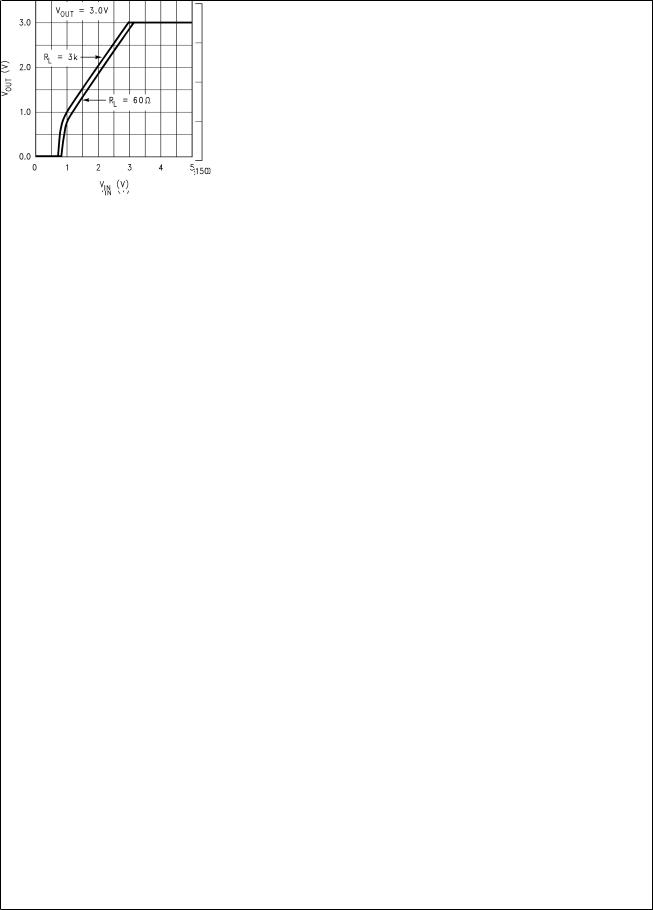
Typical Performance Characteristics Unless otherwise specified: TA = 25ÊC, VIN = VO(NOM) + 1V, COUT = 2.2 µF, all voltage options, ON/OFF pin tied to VIN.
Output Voltage vs |
Output Voltage vs |
Temperature |
Temperature |
DS012078-9 DS012078-39
Output Voltage vs |
Dropout Characteristics |
Temperature |
|
DS012078-16
|
DS012078-40 |
Dropout Characteristics |
Dropout Characteristics |
DS012078-14
DS012078-15
www.national.com |
6 |
 Loading...