


NSC LP2986AIM-3.3, LP2986AIM-3.0, LP2986IMM-3.0, LP2986IM-5.0, LP2986IM-3.0 Datasheet
...March 1999
LP2986
Micropower, 200 mA Ultra Low-Dropout Fixed or Adjustable Voltage Regulator
General Description
The LP2986 is a 200 mA precision LDO voltage regulator which offers the designer a higher performance version of the industry standard LP2951.
Using an optimized VIP™ (Vertically Integrated PNP) process, the LP2986 delivers superior performance:
Dropout Voltage: Typically 180 mV @ 200 mA load, and 1 mV @ 1 mA load.
Ground Pin Current: Typically 1 mA @ 200 mA load, and 200 µA @ 10 mA load.
Sleep Mode: The LP2986 draws less than 1 µA quiescent current when shutdown pin is pulled low.
Error Flag: The built-in error flag goes low when the output drops approximately 5% below nominal.
Precision Output: The standard product versions available can be pin-strapped (using the internal resistive divider) to provide output voltages of 5.0V, 3.3V, or 3.0V with guaranteed accuracy of 0.5% (ªAº grade) and %1 (standard grade) at room temperature.
Features
nUltra low dropout voltage
nGuaranteed 200 mA output current
nSO-8 and mini-SO8 surface mount packages
n<1 µA quiescent current when shutdown
nLow ground pin current at all loads
n0.5% output voltage accuracy (ªAº grade)
nHigh peak current capability (400 mA typical)
nWide supply voltage range (16V max)
nOvertemperature/overcurrent protection
n−40ÊC to +125ÊC junction temperature range
Applications
nCellular Phone
nPalmtop/Laptop Computer
nCamcorder, Personal Stereo, Camera
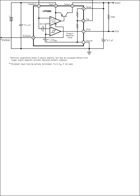
Block Diagram
DS012935-1
VIP™ is a trademark of National Semiconductor Corporation.
Regulator Voltage Adjustable or Fixed Dropout-Low Ultra mA 200 Micropower, LP2986
© 1999 National Semiconductor Corporation |
DS012935 |
www.national.com |
Connection Diagram and Ordering Information
Surface Mount Packages:
Mini SO-8 Package Type MM: See NS Package Drawing Number MUA08A
SO-8 Package Type M: See NS Package Drawing Number M08A
DS012935-2
Top View
For ordering information, refer to Table 1 of this document.
Basic Application Circuits
Application Using Internal Resistive Divider
DS012935-3
www.national.com |
2 |

Basic Application Circuits (Continued)
Application Using External Divider
|
|
|
|
|
DS012935-4 |
Ordering Information |
|
|
|||
|
|
TABLE 1. Package Marking and Ordering Information |
|
||
|
|
|
|
|
|
Output Voltage |
Grade |
|
Order Information |
Package Marking |
Supplied as: |
|
|
|
|
|
|
5 |
A |
|
LP2986AIMMX-5.0 |
L41A |
3.5k Units on Tape and Reel |
|
|
|
|
|
|
5 |
A |
|
LP2986AIMM-5.0 |
L41A |
250 Units on Tape and Reel |
|
|
|
|
|
|
5 |
STD |
|
LP2986IMMX-5.0 |
L41B |
3.5k Units on Tape and Reel |
|
|
|
|
|
|
5 |
STD |
|
LP2986IMM-5.0 |
L41B |
250 Units on Tape and Reel |
|
|
|
|
|
|
3.3 |
A |
|
LP2986AIMMX-3.3 |
L40A |
3.5k Units on Tape and Reel |
|
|
|
|
|
|
3.3 |
A |
|
LP2986AIMM-3.3 |
L40A |
250 Units on Tape and Reel |
|
|
|
|
|
|
3.3 |
STD |
|
LP2986IMMX-3.3 |
L40B |
3.5k Units on Tape and Reel |
|
|
|
|
|
|
3.3 |
STD |
|
LP2986IMM-3.3 |
L40B |
250 Units on Tape and Reel |
|
|
|
|
|
|
3.0 |
A |
|
LP2986AIMMX-3.0 |
L39A |
3.5k Units on Tape and Reel |
|
|
|
|
|
|
3.0 |
A |
|
LP2986AIMM-3.0 |
L39A |
250 Units on Tape and Reel |
|
|
|
|
|
|
3.0 |
STD |
|
LP2986IMMX-3.0 |
L39B |
3.5k Units on Tape and Reel |
|
|
|
|
|
|
3.0 |
STD |
|
LP2986IMM-3.0 |
L39B |
250 Units on Tape and Reel |
|
|
|
|
|
|
5 |
A |
|
LP2986AIMX-5.0 |
2986AIM5.0 |
2.5k Units on Tape and Reel |
|
|
|
|
|
|
5 |
A |
|
LP2986AIM-5.0 |
2986AIM5.0 |
Shipped in Anti-Static Rails |
|
|
|
|
|
|
5 |
STD |
|
LP2986IMX-5.0 |
2986IM5.0 |
2.5k Units on Tape and Reel |
|
|
|
|
|
|
5 |
STD |
|
LP2986IM-5.0 |
2986IM5.0 |
Shipped in Anti-Static Rails |
|
|
|
|
|
|
3.3 |
A |
|
LP2986AIMX-3.3 |
2986AIM3.3 |
2.5k Units on Tape and Reel |
|
|
|
|
|
|
3.3 |
A |
|
LP2986AIM-3.3 |
2986AIM3.3 |
Shipped in Anti-Static Rails |
|
|
|
|
|
|
3.3 |
STD |
|
LP2986IMX-3.3 |
2986IM3.3 |
2.5k Units on Tape and Reel |
|
|
|
|
|
|
3.3 |
STD |
|
LP2986IM-3.3 |
2986IM3.3 |
Shipped in Anti-Static Rails |
|
|
|
|
|
|
3.0 |
A |
|
LP2986AIMX-3.0 |
2986AIM3.0 |
2.5k Units on Tape and Reel |
|
|
|
|
|
|
3.0 |
A |
|
LP2986AIM-3.0 |
2986AIM3.0 |
Shipped in Anti-Static Rails |
|
|
|
|
|
|
3.0 |
STD |
|
LP2986IMX-3.0 |
2986IM3.0 |
2.5k Units on Tape and Reel |
|
|
|
|
|
|
3.0 |
STD |
|
LP2986IM-3.0 |
2986IM3.0 |
Shipped in Anti-Static Rails |
|
|
|
|
|
|
3 |
www.national.com |

Absolute Maximum Ratings (Note 1)
If Military/Aerospace specified devices are required, please contact the National Semiconductor Sales Office/ Distributors for availability and specifications.
Storage Temperature Range |
−65ÊC to +150ÊC |
Operating Junction |
|
Temperature Range |
−40ÊC to +125ÊC |
Lead Temperature |
|
(Soldering, 5 seconds) |
260ÊC |
ESD Rating (Note 2) |
2 kV |
Power Dissipation (Note 3) |
Internally Limited |
Input Supply Voltage |
|
(Survival) |
−0.3V to +16V |
Input Supply Voltage |
|
(Operating) |
2.1V to +16V |
Shutdown Pin |
−0.3V to +16V |
Feedback Pin |
−0.3V to +5V |
Output Voltage |
|
(Survival) (Note 4) |
−0.3V to +16V |
IOUT (Survival) |
Short Circuit Protected |
Input-Output Voltage |
|
(Survival) (Note 5) |
−0.3V to +16V |
Electrical Characteristics
Limits in standard typeface are for T J = 25ÊC, and limits in boldface type apply over the full operating temperature range. Unless otherwise specified: VIN = VO(NOM) + 1V, IL = 1 mA, COUT = 4.7 µF, CIN = 2.2 µF, VS/D = 2V.
|
|
|
|
|
LM2986AI-X.X |
LM2986I-X.X |
|
||
Symbol |
Parameter |
Conditions |
Typical |
(Note 6) |
(Note 6) |
Units |
|||
|
|
|
|
|
Min |
Max |
Min |
Max |
|
|
|
|
|
|
|
|
|
|
|
VO |
Output Voltage |
|
|
5.0 |
4.975 |
5.025 |
4.950 |
5.050 |
|
|
(5.0V Versions) |
0.1 mA < IL |
< 200 mA |
5.0 |
4.960 |
5.040 |
4.920 |
5.080 |
|
|
|
|
|
4.910 |
5.090 |
4.860 |
5.140 |
|
|
|
|
|
|
|
|
||||
|
|
|
|
|
|
|
|
|
|
|
Output Voltage |
|
|
3.3 |
3.283 |
3.317 |
3.267 |
3.333 |
|
|
(3.3V Versions) |
|
|
|
|
|
|
|
|
|
0.1 mA < IL |
< 200 mA |
3.3 |
3.274 |
3.326 |
3.247 |
3.353 |
V |
|
|
|
|
|
3.241 |
3.359 |
3.208 |
3.392 |
|
|
|
|
|
|
|
|
||||
|
|
|
|
|
|
|
|
|
|
|
Output Voltage |
|
|
3.0 |
2.985 |
3.015 |
2.970 |
3.030 |
|
|
(3.0V Versions) |
|
|
|
|
|
|
|
|
|
0.1 mA < IL |
< 200 mA |
3.0 |
2.976 |
3.024 |
2.952 |
3.048 |
|
|
|
|
|
|
2.946 |
3.054 |
2.916 |
3.084 |
|
|
|
|
|
|
|
|
||||
|
|
|
|
|
|
|
|
|
|
|
Output Voltage Line |
VO(NOM) + 1V £ VIN £ |
0.007 |
|
0.014 |
|
0.014 |
%/V |
|
|
Regulation |
16V |
|
|
|
|
|
||
|
|
|
0.032 |
|
0.032 |
||||
|
|
|
|
|
|
|
|
||
|
|
|
|
|
|
|
|
|
|
VIN±VO |
Dropout Voltage |
IL = 100 µA |
|
1 |
|
2.0 |
|
2.0 |
|
|
(Note 7) |
|
|
|
3.5 |
|
3.5 |
|
|
|
|
|
|
|
|
|
|||
|
|
|
|
|
|
|
|
|
|
|
|
IL = 75 mA |
|
90 |
|
120 |
|
120 |
mV |
|
|
|
|
|
170 |
|
170 |
||
|
|
|
|
|
|
|
|
||
|
|
|
|
|
|
|
|
|
|
|
|
IL = 200 mA |
|
180 |
|
230 |
|
230 |
|
|
|
|
|
|
350 |
|
350 |
|
|
|
|
|
|
|
|
|
|
||
|
|
|
|
|
|
|
|
|
|
IGND |
Ground Pin Current |
IL = 100 µA |
|
100 |
|
120 |
|
120 |
|
|
|
|
|
|
150 |
|
150 |
µA |
|
|
|
|
|
|
|
|
|||
|
|
|
|
|
|
|
|
|
|
|
|
IL = 75 mA |
|
500 |
|
800 |
|
800 |
|
|
|
|
|
|
|
||||
|
|
|
|
|
1400 |
|
1400 |
|
|
|
|
|
|
|
|
|
|
||
|
|
|
|
|
|
|
|
|
|
|
|
IL = 200 mA |
|
1 |
|
2.1 |
|
2.1 |
mA |
|
|
|
|
|
3.7 |
|
3.7 |
||
|
|
|
|
|
|
|
|
||
|
|
|
|
|
|
|
|
|
|
|
|
VS/D < 0.3V |
|
0.05 |
|
1.5 |
|
1.5 |
µA |
IO(PK) |
Peak Output Current |
VOUT ³ VO(NOM) − 5 % |
400 |
250 |
|
250 |
|
|
|
IO(MAX) |
Short Circuit Current |
RL = 0 (Steady State) |
400 |
|
|
|
|
mA |
|
|
|
(Note 11) |
|
|
|
|
|
|
|
|
|
|
|
|
|
|
|
|
|
|
|
|
|
|
|
|
|
|
|
en |
Output Noise Voltage |
BW = 300 Hz to 50 |
160 |
|
|
|
|
µV(RMS) |
|
|
(RMS) |
kHz, COUT = 10 µF |
|
|
|
|
|||
|
|
|
|
|
|
|
|||
|
Ripple Rejection |
f = 1 kHz, COUT = 10 µF |
65 |
|
|
|
|
dB |
|
|
|
|
|
|
|
|
|
||
|
|
|
|
|
|
|
|
|
|
www.national.com |
4 |
Electrical Characteristics (Continued)
Limits in standard typeface are for T J = 25ÊC, and limits in boldface type apply over the full operating temperature range. Unless otherwise specified: VIN = VO(NOM) + 1V, IL = 1 mA, COUT = 4.7 µF, CIN = 2.2 µF, VS/D = 2V.
|
|
|
|
LM2986AI-X.X |
LM2986I-X.X |
|
||
Symbol |
Parameter |
Conditions |
Typical |
(Note 6) |
(Note 6) |
Units |
||
|
|
|
|
Min |
Max |
Min |
Max |
|
|
|
|
|
|
|
|
|
|
|
Output Voltage |
(Note 9) |
20 |
|
|
|
|
ppm/ÊC |
|
Temperature Coefficient |
|
|
|
|
|
||
|
|
|
|
|
|
|
|
|
|
|
|
|
|
|
|
|
|
FEEDBACK PIN |
|
|
|
|
|
|
|
|
|
|
|
|
|
|
|
|
|
VFB |
Feedback Pin Voltage |
|
1.23 |
1.21 |
1.25 |
1.20 |
1.26 |
|
|
|
|
1.20 |
1.26 |
1.19 |
1.27 |
V |
|
|
|
|
|
|||||
|
|
|
|
|
|
|
|
|
|
|
(Note 10) |
1.23 |
1.19 |
1.28 |
1.18 |
1.29 |
|
|
|
|
|
|
|
|
|
|
|
FB Pin Voltage |
(Note 9) |
20 |
|
|
|
|
ppm/ÊC |
|
Temperature Coefficient |
|
|
|
|
|
||
|
|
|
|
|
|
|
|
|
|
|
|
|
|
|
|
|
|
IFB |
Feedback Pin Bias |
IL = 200 mA |
150 |
|
330 |
|
330 |
nA |
|
Current |
|
|
760 |
|
760 |
||
|
|
|
|
|
|
|||
|
|
|
|
|
|
|
|
|
|
FB Pin Bias Current |
(Note 9) |
0.1 |
|
|
|
|
nA/ÊC |
|
Temperature Coefficient |
|
|
|
|
|
||
|
|
|
|
|
|
|
|
|
|
|
|
|
|
|
|
|
|
SHUTDOWN INPUT |
|
|
|
|
|
|
|
|
|
|
|
|
|
|
|
|
|
VS/D |
S/D Input Voltage |
VH = O/P ON |
1.4 |
1.6 |
|
1.6 |
|
V |
|
(Note 8) |
VL = O/P OFF |
0.55 |
|
0.18 |
|
0.18 |
|
|
|
|
|
|||||
IS/D |
S/D Input Current |
VS/D = 0 |
0 |
|
−1 |
|
−1 |
µA |
|
|
VS/D = 5V |
5 |
|
15 |
|
15 |
|
|
|
|
|
|
||||
ERROR COMPARATOR |
|
|
|
|
|
|
|
|
|
|
|
|
|
|
|
|
|
IOH |
Output ªHIGHº Leakage |
VOH = 16V |
0.01 |
|
1 |
|
1 |
µA |
|
|
|
|
2 |
|
2 |
||
|
|
|
|
|
|
|
||
|
|
|
|
|
|
|
|
|
VOL |
Output ªLOWº Voltage |
VIN = VO(NOM) − 0.5V, |
150 |
|
220 |
|
220 |
mV |
|
|
IO(COMP) = 300 µA |
|
350 |
|
350 |
||
|
|
|
|
|
|
|||
VTHR |
Upper Threshold |
|
−4.6 |
−5.5 |
−3.5 |
−5.5 |
−3.5 |
|
(MAX) |
Voltage |
|
−7.7 |
−2.5 |
−7.7 |
−2.5 |
|
|
|
|
|
||||||
|
|
|
|
|
|
|
|
%VOUT |
VTHR |
Lower Threshold |
|
−6.6 |
−8.9 |
−4.9 |
−8.9 |
−4.9 |
|
(MIN) |
Voltage |
|
−13.0 |
−3.3 |
−13.0 |
−3.3 |
|
|
|
|
|
||||||
|
|
|
|
|
|
|
|
|
HYST |
Hysteresis |
|
2.0 |
|
|
|
|
|
|
|
|
|
|
|
|
|
|
Note 1: Absolute Maximum Ratings indicate limits beyond which damage to the component may occur. Electrical specifications do not apply when operating the device outside of its rated operating conditions.
Note 2: The ESD rating of the Feedback pin is 500V and the Tap pin is 1.5 kV.
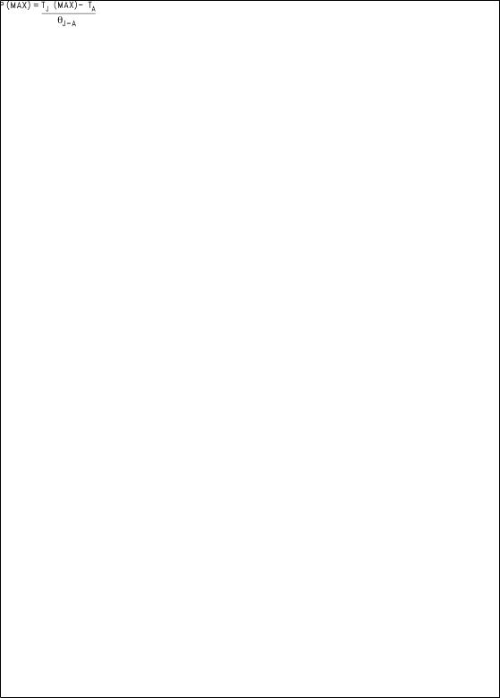
Note 3: The maximum allowable power dissipation is a function of the maximum junction temperature, TJ(MAX), the junction-to-ambient thermal resistance, θJ−A , and the ambient temperature, TA. The maximum allowable power dissipation at any ambient temperature is calculated using:
The value of θJ−A for the SO-8 (M) package is 160ÊC/W, and the mini SO-8 (MM) package is 200ÊC/W. Exceeding the maximum allowable power dissipation will cause excessive die temperature, and the regulator will go into thermal shutdown.
Note 4: If used in a dual-supply system where the regulator load is returned to a negative supply, the LM2986 output must be diode-clamped to ground.
Note 5: The output PNP structure contains a diode between the V IN and VOUT terminals that is normally reverse-biased. Forcing the output above the input will turn on this diode and may induce a latch-up mode which can damage the part (see Application Hints).
Note 6: Limits are 100% production tested at 25ÊC. Limits over the operating temperature range are guaranteed through correlation using Statistical Quality Control (SQC) methods. The limits are used to calculate National's Average Outgoing Quality Level (AOQL).
Note 7: Dropout voltage is defined as the input to output differential at which the output voltage drops 100 mV below the value measured with a 1V differential.
Note 8: To prevent mis-operation, the Shutdown input must be driven by a signal that swings above VH and below VL with a slew rate not less than 40 mV/µs (see Application Hints).
Note 9: Temperature coefficient is defined as the maximum (worst-case) change divided by the total temperature range.
Note 10: VFB ≤ VOUT ≤ (VIN − 1), 2.5V ≤ VIN ≤ 16V, 100 µA ≤ IL ≤ 200 mA, TJ ≤ 125ÊC.
Note 11: See Typical Performance Characteristics curves.
5 |
www.national.com |
 Loading...