


NSC LP3986TL-3333, LP3986TL-2929, LP3986TL-285285, LP3986TL-2828, LP3986BLX285285 Datasheet
...May 2003
LP3986
Dual Micropower 150 mA Ultra Low-Dropout CMOS Voltage Regulators in micro SMD Package
General Description
The LP3986 is a 150 mA dual low dropout regulator designed for portable and wireless applications with demanding performance and board space requirements.
The LP3986 is stable with a small 1 µF ±30% ceramic output capacitor requiring smallest possible board space.
The LP3986’s performance is optimized for battery powered systems to deliver ultra low noise, extremely low dropout voltage and low quiescent current independent of load current. Regulator ground current increases very slightly in dropout, further prolonging the battery life. Optional external bypass capacitor reduces the output noise further without slowing down the load transient response. Fast start-up time is achieved by utilizing a speed-up circuit that actively precharges the bypass capacitor. Power supply rejection is better than 60 dB at low frequencies and 55 dB at 10 kHz. High power supply rejection is maintained at low input voltage levels common to battery operated circuits.
The LP3986 is available in a micro SMD package. Performance is specified for a −40˚C to +125˚C temperature range. For single LDO applications, please refer to the LP3985 datasheet.
Features
nMiniature 8-I/O micro SMD package
nStable with 1µF ceramic and high quality tantalum output capacitors
nFast turn-on
nTwo independent regulators
nLogic controlled enable
nOver current and thermal protection
Key Specifications
nGuaranteed 150 mA output current per regulator
n1nA typical quiescent current when both regulators in shutdown mode
n60 mV typical dropout voltage at 150 mA output current
n115 µA typical ground current
n40 µV typical output noise
n200 µs fast turn-on circuit
n−40˚C to +125˚C junction temperature
Applications
nCDMA cellular handsets
nGSM cellular handsets
nPortable information appliances
nPortable battery applications
Typical Application Circuit
20003401
SMD micro in Regulators Voltage CMOS Dropout-Low Ultra mA 150 Micropower Dual LP3986
Package
© 2003 National Semiconductor Corporation |
DS200034 |
www.national.com |

LP3986
Block Diagram
LP3986
20003402
Pin Description
Name |
*micro SMD |
Function |
|
|
|
VOUT2 |
A1 |
Output Voltage of the second LDO |
EN2 |
B1 |
Enable input for the second LDO |
BYPASS |
C1 |
Bypass capacitor for the bandgap |
|
|
|
GND |
C2 |
Common ground |
|
|
|
GND |
C3 |
Common ground |
|
|
|
EN1 |
B3 |
Enable input for the first LDO |
VOUT1 |
A3 |
Output Voltage of the first LDO |
VIN |
A2 |
Common input for both LDOs |
* Note: The pin numbering scheme for the micro SMD package was revised in April 2002 to conform to JEDEC standard. Only the pin numbers were revised. No changes to the physical location of the inputs/outputs were made. For reference purposes, the obsolete
numbering scheme had VOUT2 as pin 1, EN2 as pin 2, BYPASS as pin 3, GND as pins 4 and 5, EN1 as pin 6, VOUT1 as pin 7, and VIN as pin 8.
Connection Diagram
20003404
Top View
8 Bump micro SMD Package See NS Package Number BLA08
www.national.com |
2 |
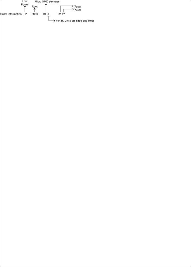
Ordering Information
For micro SMD Package (BL has thickness of 0.995mm)
Output |
Grade |
Package |
LP3986 Supplied as 250 Units, |
LP3986 Supplied as 3000 |
|
Voltage (V) |
Marking |
Tape and Reel |
Units, Tape and Reel |
||
|
|||||
|
|
|
|
|
|
2.52.8 |
STD |
14 |
LP3986BL-2528 |
LP3986BLX-2528 |
|
|
|
|
|
|
|
2.82.8 |
STD |
10 |
LP3986BL-2828 |
LP3986BLX-2828 |
|
|
|
|
|
|
|
2.852.85 |
STD |
11 |
LP3986BL-285285 |
LP3986BLX285285 |
|
|
|
|
|
|
|
2.92.9 |
STD |
15 |
LP3986BL-2929 |
LP3986BLX-2929 |
|
|
|
|
|
|
|
3.03.0 |
STD |
12 |
LP3986BL-3030 |
LP3986BLX-3030 |
|
|
|
|
|
|
|
3.13.1 |
STD |
13 |
LP3986BL-3131 |
LP3986BLX-3131 |
|
|
|
|
|
|
|
3.13.3 |
STD |
16 |
LP3986BL-3133 |
LP3986BLX-3133 |
|
|
|
|
|
|
|
3.33.3 |
STD |
17 |
LP3986BL-3333 |
LP3986BLX-3333 |
|
|
|
|
|
|
For micro SMD Package (TL has thickness of 0.600mm)
Output |
Grade |
Package |
LP3986 Supplied as 250 Units, |
LP3986 Supplied as 3000 |
|
Voltage (V) |
Marking |
Tape and Reel |
Units, Tape and Reel |
||
|
|||||
|
|
|
|
|
|
2.52.8 |
STD |
14 |
LP3986TL-2528 |
LP3986TLX-2528 |
|
|
|
|
|
|
|
2.82.8 |
STD |
10 |
LP3986TL-2828 |
LP3986TLX-2828 |
|
|
|
|
|
|
|
2.852.85 |
STD |
11 |
LP3986TL-285285 |
LP3986TLX285285 |
|
|
|
|
|
|
|
2.92.9 |
STD |
15 |
LP3986TL-2929 |
LP3986TLX-2929 |
|
|
|
|
|
|
|
3.03.0 |
STD |
12 |
LP3986TL-3030 |
LP3986TLX-3030 |
|
|
|
|
|
|
|
3.13.1 |
STD |
13 |
LP3986TL-3131 |
LP3986TLX-3131 |
|
|
|
|
|
|
|
3.13.3 |
STD |
16 |
LP3986TL-3133 |
LP3986TLX-3133 |
|
|
|
|
|
|
|
3.33.3 |
STD |
17 |
LP3986TL-3333 |
LP3986TLX-3333 |
|
|
|
|
|
|
20003403
LP3986
3 |
www.national.com |

LP3986
Absolute Maximum Ratings (Notes 1,
2)
If Military/Aerospace specified devices are required, please contact the National Semiconductor Sales Office/ Distributors for availability and specifications.
VIN, VEN |
−0.3 to 6.5V |
VOUT |
−0.3 to (VIN+0.3V) ≤ 6.5V |
Junction Temperature |
150˚C |
Storage Temperature |
−65˚C to +150˚C |
Pad Temp. (Note 3) |
235˚C |
Maximum Power Dissipation |
|
(Note 4) |
364mW |
ESD Rating (Note 5) |
|
Human Body Model |
2kV |
Machine Model |
200V |
Operating Ratings (Notes 1, 2)
VIN |
2.5 to 6V |
VEN |
0 to (VIN+ 0.3V) ≤ 6V |
Junction Temperature |
−40˚C to +125˚C |
Thermal Resistance |
|
θJA |
220˚C/W |
Maximum Power Dissipation (Note 6) |
250mW |
Electrical Characteristics
Unless otherwise specified: VIN = VOUT(nom) + 0.5V, CIN = 1 µF, IOUT = 1mA, COUT = 1 µF, CBYPASS = 0.01µF. Typical values and limits appearing in standard typeface are for TJ = 25˚C. Limits appearing in boldface type apply over the entire junction
temperature range for operation, −40˚C to +125˚C. (Note 7) (Note 8)
Symbol |
Parameter |
Conditions |
Typ |
|
Limit |
Units |
|
|
|
|
|||||
Min |
|
Max |
|||||
|
|
|
|
|
|
||
|
|
|
|
|
|
|
|
|
Output Voltage |
IOUT = 1mA |
|
−2.5 |
|
2.5 |
% of |
|
Tolerance |
|
|
−3.0 |
|
3.0 |
VOUT(nom) |
|
Line Regulation Error |
VIN = (VOUT(nom) + 0.5V) to |
0.006 |
|
|
0.092 |
|
∆VOUT |
(Note 9) |
6.0V, |
|
|
|
0.128 |
%/V |
|
|
IOUT = 1 mA |
|
|
|
|
|
|
Load Regulation Error |
IOUT = 1mA to 150 mA |
0.003 |
|
|
0.006 |
%/mA |
|
(Note 10) |
|
|
|
|
0.01 |
|
|
|
|
|
|
|
||
|
|
|
|
|
|
|
|
|
Output AC Line |
VIN = VOUT(nom) + 1V, |
1.5 |
|
|
|
mVP-P |
|
Regulation |
IOUT = 150 mA (Figure 1) |
|
|
|
|
|
|
|
|
|
|
|
||
|
|
VIN = 3.1V, |
60 |
|
|
|
|
|
|
f = 1 kHz, |
|
|
|
|
|
PSRR |
Power Supply Rejection |
IOUT = 50 mA (Figure 2) |
|
|
|
|
dB |
Ratio |
VIN = 3.1V, |
50 |
|
|
|
||
|
|
|
|
|
|||
|
|
f = 10 kHz, |
|
|
|
|
|
|
|
IOUT = 50 mA (Figure 2) |
|
|
|
|
|
IQ |
Quiescent Current |
Both Regulators ON |
115 |
|
|
200 |
|
|
|
VEN = 1.4V, IOUT = 0 mA |
|
|
|
|
|
|
|
Both Regulators ON |
220 |
|
|
320 |
|
|
|
VEN = 1.4V, IOUT = 0 to 150 |
|
|
|
|
|
|
|
mA |
|
|
|
|
|
|
|
|
|
|
|
|
|
|
|
One Regulator ON |
75 |
|
|
130 |
µA |
|
|
VEN = 1.4V IOUT = 0 mA |
|
|
|
|
|
|
|
|
|
|
|
|
|
|
|
One Regulator ON |
130 |
|
|
200 |
|
|
|
VEN = 1.4V IOUT = 0 to 150 |
|
|
|
|
|
|
|
mA |
|
|
|
|
|
|
|
|
|
|
|
|
|
|
|
VEN = 0.4V, Both Regulators |
0.001 |
|
|
2 |
|
|
|
OFF (shutdown) |
|
|
|
4 |
|
|
|
|
|
|
|
|
|
|
Dropout Voltage |
IOUT = 1 mA |
0.4 |
|
|
2 |
mV |
|
(Note 11) |
IOUT = 150 mA |
60 |
|
|
100 |
|
|
|
|
|
||||
ISC |
Short Circuit Current |
Output Grounded |
600 |
|
|
|
mA |
|
Limit |
|
|
|
|
|
|
|
|
|
|
|
|
|
|
|
|
|
|
|
|
|
|
IOUT(PK) |
Peak Output Current |
VOUT ≥ VOUT(nom) - 5% |
500 |
300 |
|
|
mA |
TON |
Turn-On Time |
CBYPASS = 0.01 µF |
200 |
|
|
|
µs |
|
(Note 12) |
|
|
|
|
|
|
|
|
|
|
|
|
|
|
|
|
|
|
|
|
|
|
www.national.com |
4 |
 Loading...