


NSC LMV339MX, LMV339MTX, LMV339MT, LMV339M, LMV331M7X Datasheet
...August 1999
LMV331 Single / LMV393 Dual / LMV339 Quad General Purpose, Low Voltage, TinyPack Comparators
General Description
The LMV393 and LMV339 are low voltage (2.7-5V) versions of the dual and quad comparators, LM393/339, which are specified at 5-30V. The LMV331 is the single version, which is available in space saving SC70-5 and SOT23-5 packages. SC70-5 is approximately half the size of SOT23-5.
The LMV393 is available in 8-pin SOIC and 8-pin MSOP. The LMV339 is available in 14-pin SOIC and 14-pin TSSOP.
The LMV331/393/339 is the most cost-effective solution where space, low voltage, low power and price are the primary specification in circuit design for portable consumer products. They offer specifications that meet or exceed the familiar LM393/339 at a fraction of the supply current.
The chips are built with National's advanced Submicron Silicon-Gate BiCMOS process. The LMV331/393/339 have bipolar input and output stages for improved noise performance.
Features
(For 5V Supply, Typical Unless Otherwise Noted)
nSpace Saving SC70-5 Package (2.0 x 2.1 x 1.0 mm)
nSpace Saving SOT23-5 Package (3.00 x 3.01 x
1.43mm)
nGuaranteed 2.7V and 5V Performance
n |
Industrial Temperature Range |
−40ÊC to +85ÊC |
n |
Low Supply Current |
60µA/Channel |
n Input Common Mode Voltage Range Includes Ground |
||
n Low Output Saturation Voltage |
200 mV |
|
Applications
nMobile Communications
nNotebooks and PDA's
nBattery Powered Electronics
nGeneral Purpose Portable Device
nGeneral Purpose Low Voltage Applications
Connection Diagrams
5-Pin SC70-5/SOT23-5 |
14-Pin SO/TSSOP |
DS100080-1
Top View
8-Pin SO/MSOP
DS100080-3
Top View
DS100080-2
Top View
TinyPack Voltage, Low Purpose, General Quad LMV339 / Dual LMV393 / Single LMV331
Comparators
© 1999 National Semiconductor Corporation |
DS100080 |
www.national.com |

Ordering Information
|
Temperature Range |
Packaging |
|
Transport |
NSC |
Package |
|
Marking |
|
Media |
Drawing |
Industrial |
|
||||
|
−40ÊC to +85ÊC |
|
|
|
|
|
|
|
|
|
|
5-pin SC70-5 |
LMV331M7 |
C13 |
1k |
Units Tape and Reel |
MAA05 |
|
|
|
|
|
|
|
LMV331M7X |
C13 |
3k |
Units Tape and Reel |
|
|
|
|
|
|
|
5-pin SOT23-5 |
LMV331M5 |
C12 |
1k |
Units Tape and Reel |
MA05B |
|
|
|
|
|
|
|
LMV331M5X |
C12 |
3k |
Units Tape and Reel |
|
|
|
|
|
|
|
8-pin Small Outline |
LMV393M |
LMV393M |
Rails |
M08A |
|
|
|
|
|
|
|
|
LMV393MX |
LMV393M |
2.5k Units Tape and Reel |
||
|
|
||||
|
|
|
|
|
|
8-pin MSOP |
LMV393MM |
LMV393 |
1k |
UnitsTape and Reel |
MUA08A |
|
|
|
|
|
|
|
LMV393MMX |
LMV393 |
3.5k Units Tape and Reel |
||
|
|
||||
|
|
|
|
|
|
14-pin Small Outline |
LMV339M |
LMV339M |
Rails |
M14A |
|
|
|
|
|
|
|
|
LMV339MX |
LMV339M |
2.5k Units Tape and Reel |
||
|
|
||||
|
|
|
|
|
|
14-pin TSSOP |
LMV339MT |
LMV339MT |
Rails |
MTC14 |
|
|
|
|
|
|
|
|
LMV339MTX |
LMV339MT |
2.5k Units Tape and Reel |
||
|
|
||||
|
|
|
|
|
|
www.national.com |
2 |

Absolute Maximum Ratings (Note 1)
If Military/Aerospace specified devices are required, please contact the National Semiconductor Sales Office/ Distributors for availability and specifications.
ESD Tolerance (Note 2) |
|
Human Body Model |
|
LMV331/ 393/ 339 |
800V |
Machine Model LMV331/339/393 |
120V |
Differential Input Voltage |
± Supply Voltage |
Voltage on any pin |
5.5V |
(referred to V− pin) |
|
Soldering Information |
|
Infrared or Convection (20 sec) |
235ÊC |
Storage Temp. Range |
−65ÊC to +150ÊC |
Junction Temperature (Note 3) |
150ÊC |
Operating Ratings(Note 1)
Supply Voltage |
2.7V to 5.0V |
Temperature Range |
|
LMV393, LMV339, |
−40ÊC ≤ TJ ≤ +85ÊC |
LMV331 |
|
Thermal Resistance (θJA) |
|
M Package, 8-pin Surface |
190ÊC/W |
Mount |
|
M Package, 14-pin Surface |
145ÊC/W |
Mount |
|
MTC Package, 14-pin |
155ÊC/W |
TSSOP |
|
MAA05 Package, 5-pin |
478ÊC/W |
SC70-5 |
|
M05A Package 5 -pin |
265ÊC/W |
SOT23-5 |
|
MM Package, 8-pin Mini |
235ÊC/W |
Surface Mount |
|
2.7V DC Electrical Characteristics
Unless otherwise specified, all limits guaranteed for TJ = 25ÊC, V+ = 2.7V, V− |
= 0V. Boldface limits apply at the temperature |
||||||
extremes. |
|
|
|
|
|
|
|
Symbol |
|
Parameter |
Conditions |
|
Typ |
LMV331/ |
Units |
|
|
|
|
(Note 4) |
393/339 |
|
|
|
|
|
|
|
|
Limit |
|
|
|
|
|
|
|
(Note 5) |
|
|
|
|
|
|
|
|
|
VOS |
|
Input Offset Voltage |
|
|
1.7 |
7 |
mV |
|
|
|
|
|
max |
||
|
|
|
|
|
|
|
|
|
|
|
|
|
|
|
|
TCVOS |
|
Input Offset Voltage |
|
|
5 |
|
µV/ÊC |
|
|
Average Drift |
|
|
|
||
|
|
|
|
|
|
|
|
|
|
|
|
|
|
|
|
IB |
|
Input Bias Current |
|
|
10 |
250 |
nA max |
|
|
|
|
|
400 |
||
|
|
|
|
|
|
|
|
|
|
|
|
|
|
|
|
IOS |
|
Input Offset Current |
|
|
5 |
50 |
nA max |
|
|
|
|
|
150 |
|
|
|
|
|
|
|
|
|
|
|
|
|
|
|
|
|
|
VCM |
|
Input Voltage Range |
|
|
−0.1 |
|
V |
|
|
|
|
|
2.0 |
|
V |
|
|
|
|
|
|
|
|
VSAT |
|
Saturation Voltage |
Isink ≤ 1mA |
|
200 |
|
mV |
IO |
|
Output Sink Current |
VO ≤ 1.5V |
|
23 |
5 |
mA min |
IS |
|
Supply Current |
LMV331 |
|
40 |
100 |
µA max |
|
|
|
LMV393 |
|
70 |
140 |
µA max |
|
|
|
Both Comparators |
|
|
|
|
|
|
|
|
|
|
|
|
|
|
|
LMV339 |
|
140 |
200 |
µA max |
|
|
|
All four Comparators |
|
|
|
|
|
|
|
|
|
|
|
|
|
|
Output Leakage Current |
|
|
.003 |
1 |
µA max |
|
|
|
|
|
|
|
|
2.7V AC Electrical Characteristics
TJ = 25ÊC, V+ = 2.7V, RL = 5.1 kΩ, V− = 0V.
Symbol |
Parameter |
Conditions |
Typ |
Units |
|
|
|
(Note 4) |
|
|
|
|
|
|
tPHL |
Propagation Delay (High to Low) |
Input Overdrive =10 mV |
1000 |
ns |
|
|
Input Overdrive =100 mV |
350 |
ns |
|
|
|
|
|
tPLH |
Propagation Delay (Low to High) |
Input Overdrive =10 mV |
500 |
ns |
|
|
Input Overdrive =100 mV |
400 |
ns |
|
|
|
|
|
3 |
www.national.com |

5V DC Electrical Characteristics
Unless otherwise specified, all limits guaranteed for TJ = 25ÊC, V+ = 5V, V− |
= 0V. Boldface limits apply at the temperature |
||||||
extremes. |
|
|
|
|
|
|
|
|
|
|
|
|
|
|
|
Symbol |
|
Parameter |
Conditions |
|
Typ |
LMV331/ |
Units |
|
|
|
|
|
(Note 4) |
393/339 |
|
|
|
|
|
|
|
Limit |
|
|
|
|
|
|
|
(Note 5) |
|
|
|
|
|
|
|
|
|
VOS |
|
Input Offset Voltage |
|
|
1.7 |
7 |
mV |
|
|
|
|
|
|
9 |
max |
|
|
|
|
|
|
|
|
TCVOS |
|
Input Offset Voltage |
|
|
5 |
|
µV/ÊC |
|
|
Average Drift |
|
|
|
||
|
|
|
|
|
|
|
|
|
|
|
|
|
|
|
|
IB |
|
Input Bias Current |
|
|
25 |
250 |
nA max |
|
|
|
|
|
400 |
||
|
|
|
|
|
|
|
|
|
|
|
|
|
|
|
|
IOS |
|
Input Offset Current |
|
|
2 |
50 |
nA max |
|
|
|
|
|
150 |
|
|
|
|
|
|
|
|
|
|
|
|
|
|
|
|
|
|
VCM |
|
Input Voltage Range |
|
|
−0.1 |
|
V |
|
|
|
|
|
4.2 |
|
V |
|
|
|
|
|
|
|
|
AV |
|
Voltage Gain |
|
|
50 |
20 |
V/mV min |
Vsat |
|
Saturation Voltage |
Isink ≤ 4 mA |
|
200 |
400 |
mV |
|
|
|
|
|
|
700 |
max |
|
|
|
|
|
|
|
|
IO |
|
Output Sink Current |
VO ≤ 1.5V |
|
84 |
10 |
mA |
IS |
|
Supply Current |
LMV331 |
|
60 |
120 |
µA max |
|
|
|
|
|
|
150 |
|
|
|
|
|
|
|
|
|
|
|
|
LMV393 |
|
100 |
200 |
µA max |
|
|
|
Both Comparators |
|
|
250 |
|
|
|
|
|
|
|
|
|
|
|
|
LMV339 |
|
170 |
300 |
µA max |
|
|
|
All four Comparators |
|
|
350 |
|
|
|
|
|
|
|
|
|
|
|
Output Leakage Current |
|
|
.003 |
1 |
µA max |
|
|
|
|
|
|
|
|
5V AC Electrical Characteristics
TJ = 25ÊC, V+ = 5V, RL = 5.1 kΩ, V− = 0V.
Symbol |
Parameter |
Conditions |
Typ |
Units |
|
|
|
(Note 4) |
|
|
|
|
|
|
tPHL |
Propagation Delay (High to Low) |
Input Overdrive =10 mV |
600 |
ns |
|
|
Input Overdrive =100 mV |
200 |
ns |
|
|
|
|
|
tPLH |
Propagation Delay (Low to High) |
Input Overdrive =10 mV |
450 |
ns |
|
|
Input Overdrive =100 mV |
300 |
ns |
|
|
|
|
|
Note 1: Absolute Maximum Ratings indicate limits beyond which damage to the device may occur. Operating Ratings indicate conditions for which the device is intended to be functional, but specific performance is not guaranteed. For guaranteed specifications and the test conditions, see the Electrical characteristics.
Note 2: : Human body model, 1.5kΩ in series with 100 pF. Machine model, 200Ω in series with 100 pF.
Note 3: The maximum power dissipation is a function of TJ(max), θJA, and TA. The maximum allowable power dissipation at any ambient temperature is PD = (TJ(max) - TA)/θJA. All numbers apply for packages soldered directly into a PC board.
Note 4: Typical Values represent the most likely parametric norm.
Note 5: All limits are guaranteed by testing or statistical analysis.
www.national.com |
4 |
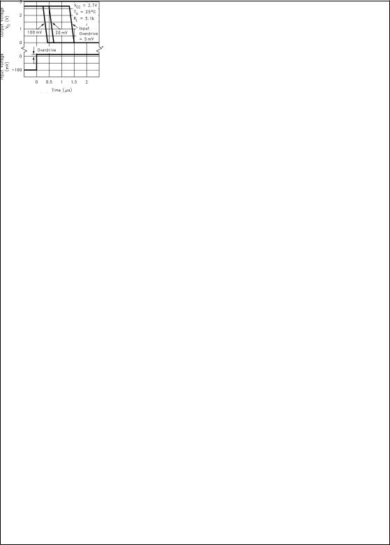
Typical Performance Characteristics Unless otherwise specified, VS = +5V, single supply, TA = 25ÊC
Supply Current vs |
Supply Current vs |
|
|
Supply Voltage Output High |
|
||
Supply Voltage Output Low |
Output Voltage vs |
||
(LMV331) |
|||
(LMV331) |
Output Current at 5V Supply |
||
|
DS100080-34 |
DS100080-33 |
DS100080-37 |
|
Output Voltage vs |
Input Bias Current vs |
Response Time vs |
|
Output Current |
|||
Supply Voltage |
Input Overdrives |
||
at 2.7 Supply |
|||
|
Negative Transition |
||
|
|
|
DS100080-36 |
DS100080-38 |
DS100080-42 |
|
Response Time for |
Response Time vs |
Response Time for |
|
Input Overdrive |
|||
Input Overdrives |
|||
Input Overdrive |
|||
Positive Transition |
|||
Negative Transition |
|||
Positive Transition |
|||
|
|||
|
|
DS100080-43
DS100080-41
DS100080-40
5 |
www.national.com |

Simplified Schematic
DS100080-47
www.national.com |
6 |

Application Circuits
Basic Comparator
A basic comparator circuit is used for converting analog signals to a digital output. The LMV331/393/339 have an open-collector output stage, which requires a pull-up resistor to a positive supply voltage for the output to switch properly. When the internal output transistor is off, the output voltage will be pulled up to the external positive voltage.
The output pull-up resistor should be chosen high enough so as to avoid excessive power dissipation yet low enough to supply enough drive to switch whatever load circuitry is used on the comparator output. On the LMV331/393/339 the pull-up resistor should range between 1k to 10kΩ.
The comparator compares the input voltage (Vin) at the
non-inverting pin to the reference voltage (Vref) at the inverting pin. If Vin is less than Vref, the output voltage (Vo) is at the saturation voltage. On the other hand, if Vin is greater than
Vref, the output voltage (Vo) is at Vcc..
DS100080-26
DS100080-4
FIGURE 1. Basic Comparator
Comparator with Hysteresis
The basic comparator configuration may oscillate or produce a noisy output if the applied differential input voltage is near the comparator's offset voltage. This usually happens when the input signal is moving very slowly across the comparator's switching threshold. This problem can be prevented by the addition of hysteresis or positive feedback.
Inverting Comparator with Hysteresis
The inverting comparator with hysteresis requires a three resistor network that are referenced to the supply voltage Vcc of the comparator. When Vin at the inverting input is less than Va, the voltage at the non-inverting node of the comparator (Vin < Va), the output voltage is high (for simplicity assume Vo switches as high as Vcc). The three network resistors can be represented as R1//R3 in series with R2. The lower input trip voltage Va1 is defined as
When Vin is greater than Va (Vin Va), the output voltage is low very close to ground. In this case the three network resistors can be presented as R2//R3 in series with R1. The upper trip voltage Va2 is defined as
The total hysteresis provided by the network is defined as Va = Va1 - Va2
To assure that the comparator will always switch fully to Vcc and not be pulled down by the load the resistors values should be chosen as follow:
Rpull-up << Rload and R1 > Rpull-up.
7 |
www.national.com |
 Loading...