


LM3704XDMMX-232
NSC LM3704XDMMX-232, LM3704XDMMX-220, LM3704XDMM-463, LM3704XDBPX-463, LM3704XDBPX-232 Datasheet
...
LM3704/LM3705
Microprocessor Supervisory Circuits with Power Fail
Input, Low Line Output and Manual Reset
General Description
The LM3704/LM3705 series of microprocessor supervisory
circuits provide the maximum flexibility for monitoring power
supplies and battery controlled functions in systems without
backup batteries. The LM3704/LM3705 series are available
in MSOP-10 and 9-bump micro SMD packages.
Built-in features include the following:
Reset: Reset is asserted during power-up, power-down, and
brownout conditions. RESET is guaranteed down to V
CC
of
1.0V.
Manual Reset Input: An input that asserts reset when pulled
low.
Power-Fail Input: A 1.225V threshold detector for power fail
warning, or to monitor a power supply other than V
CC
.
Low Line Output: This early power failure warning indicator
goes low when the supply voltage drops to a value which is
2% higher than the reset threshold voltage.
Features
n Standard Reset Threshold voltage: 3.08V
n Custom Reset Threshold voltages: For other voltages
between 2.2V and 5.0V in 10mV increments, contact
National Semiconductor Corp.
n No external components required
n Manual-Reset input
n RESET (LM3704) or RESET (LM3705) outputs
n Precision supply voltage monitor
n Factory programmable Reset Timeout Delay
n Separate Power Fail comparator
n Available in micro SMD package for minimum footprint
n
±
0.5% Reset threshold accuracy at room temperature
n
±
2% Reset threshold accuracy over temperature
extremes
n Reset assertion down to 1V V
CC
(RESET option only)
n 28 µA VCCsupply current
Applications
n Embedded Controllers and Processors
n Intelligent Instruments
n Automotive Systems
n Critical µP Power Monitoring
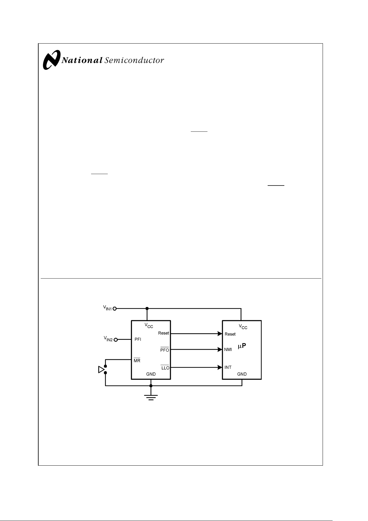
Typical Application
10136903
July 2002
LM3704/LM3705 Microprocessor Supervisory Circuits with Power Fail Input, Low Line Output and
Manual Reset
© 2002 National Semiconductor Corporation DS101369 www.national.com
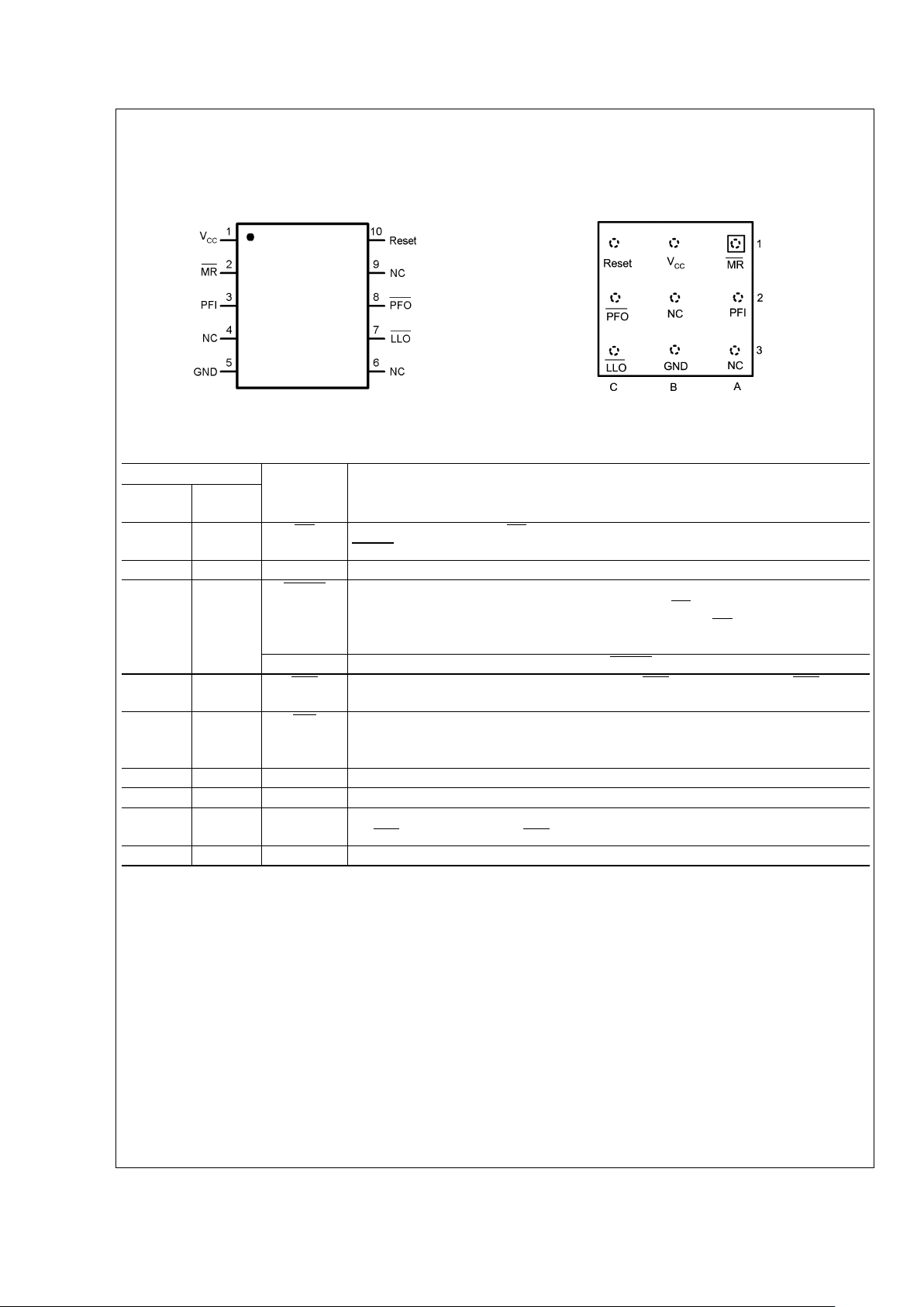
Connection Diagram
MSOP-10
Top View
(looking from the coating side)
micro SMD 9 Bump Package
BPA09
10136902
10136901
Pin Description
Pin No.
Name Function
micro
SMD
MSOP
A1 2 MR
Manual-Reset input. When MR is less than V
MRT
(Manual Reset Threshold)
RESET/RESET is engaged.
B1 1 V
CC
Power Supply input.
C1 10 RESET
Reset Logic Output. Pulses low for tRP(Reset Timeout Period) when triggered, and stays
low whenever V
CC
is below the reset threshold or when MR is below V
MRT
. It remains low
for tRPafter either VCCrises above the reset threshold, or after MR input rises above
V
MRT
(LM3704 only).
RESET Reset Logic Output. RESET is the inverse of RESET (LM3705 only).
C2 8 PFO Power-Fail Logic Output. When PFI is below V
PFT
, PFO goes low; otherwise, PFO
remains high.
C3 7 LLO
Low-Line Logic Output. Early Power-Fail warning output. Low when VCCfalls below V
LLOT
(Low-Line Output Threshold). This output can be used to generate an NMI (Non-Maskable
Interrupt) to provide an early warning of imminent power-failure.
B3 5 GND Ground reference for all signals.
A3 4, 6 NC No Connect.
A2 3 PFI Power-Fail Comparator Input. When PFI is less than V
PFT
(Power-Fail Reset Threshold),
the PFO goes low; otherwise, PFO remains high.
B2 9 NC No Connect. Test input used at factory only. Leave floating.
LM3704/LM3705
www.national.com 2
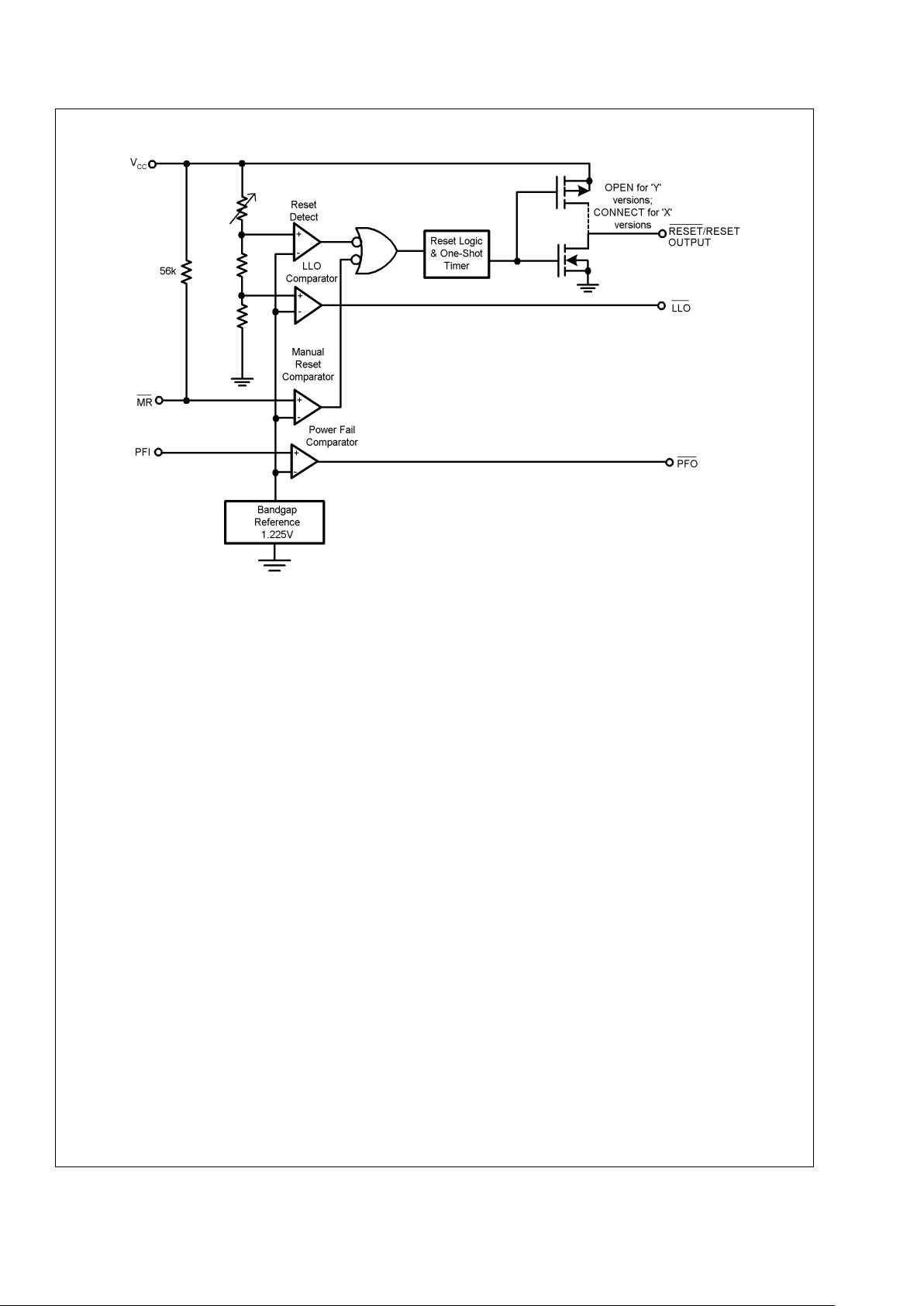
Block Diagram
10136926
LM3704/LM3705
www.national.com3
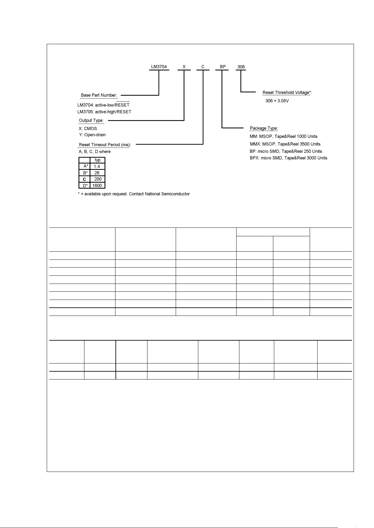
Ordering Information
10136904
*
For other voltages between 2.2V and 5.0V, please contact National Semiconductor sales office.
LM3704/LM3705
Part Number Output
Reset Timeout
Period
Package
Package
Marking
MSOP
micro
SMD
LM3704XCBP-308 totem-pole 200ms x %%I4
LM3704XCBPX-308 totem-pole 200ms x %%I4
LM3704XCMM-308 totem-pole 200ms x R35B
LM3704XCMMX-308 totem-pole 200ms x R35B
LM3705XCBP-308 totem-pole 200ms x %%I5
LM3705XCBPX-308 totem-pole 200ms x %%I5
LM3705XCMM-308 totem-pole 200ms x R36B
LM3705XCMMX-308 totem-pole 200ms x R36B
%% is the datecode and will vary with time.
Table Of Functions
Part
Number
Active
Low
Reset
Active
High
Reset
Output
(X = totem-pole)
(Y = open-drain)
Reset
Timeout
Period
Manual
Reset
Power Fail
Comparator
Low
Line
Output
LM3704 x X, Y
*
Customized x x x
LM3705 x X Customized x x x
*
= available upon request. Contact National
LM3704/LM3705
www.national.com 4
Absolute Maximum Ratings (Note 1)
If Military/Aerospace specified devices are required,
please contact the National Semiconductor Sales Office/
Distributors for availability and specifications.
Supply Voltage (V
CC
) −0.3V to 6.0V
All Other Inputs −0.3V to V
CC
+ 0.3V
ESD Ratings (Note 2)
Human Body Model
Machine Model
1.5kV
150V
Power Dissipation (Note 3)
Operating Ratings (Note 1)
Temperature Range −40˚C ≤ T
J
≤ 85˚C
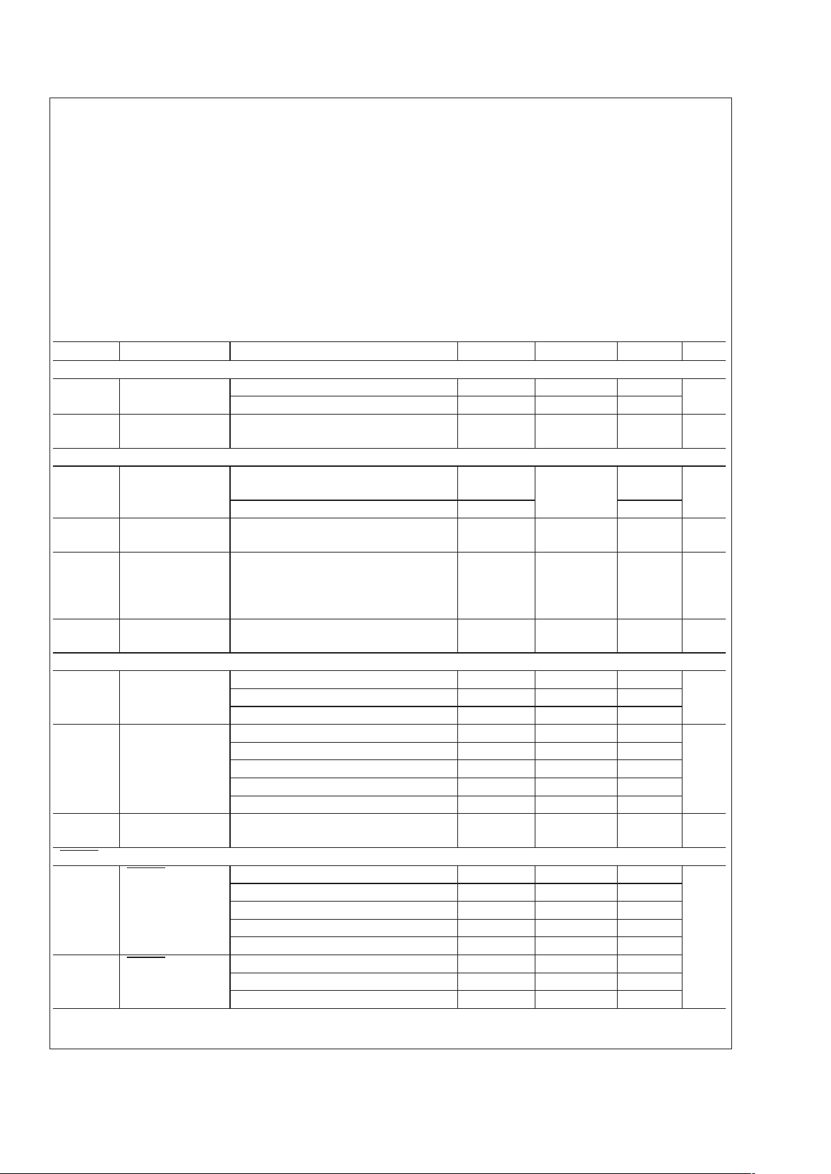
LM3704/LM3705 Series Electrical Characteristics
Limits in the standard typeface are for TJ= 25˚C and limits in boldface type apply over full operating range. Unless otherwise
specified: V
CC
= +2.2V to 5.5V.
Symbol Parameter Conditions Min Typ Max Units
POWER SUPPLY
V
CC
Operating Voltage
Range: V
CC
LM3704 1.0 5.5
V
LM3705 1.2 5.5
I
CC
VCCSupply
Current
All inputs = VCC; all outputs floating 28 50 µA
RESET THRESHOLD
V
RST
Reset Threshold VCCfalling −0.5
−2
V
RST
+0.5
+2
%
V
CC
falling: TA= 0˚C to 70˚C −1.5 +1.5
V
RSTH
Reset Threshold
Hysteresis
0.0032•V
RST
mV
t
RP
Reset Timeout
Period
Reset Timeout Period = A
Reset Timeout Period = B
Reset Timeout Period = C
Reset Timeout Period = D
1
20
140
1120
1.4
28
200
1600
2
40
280
2240
ms
t
RD
VCCto Reset
Delay
VCCfalling at 1mV/µs 20 µs
RESET (LM3705)
V
OL
RESET V
CC
>
2.25V, I
SINK
= 900µA 0.3
VV
CC
>
2.7V, I
SINK
= 1.2mA 0.3
V
CC
>
4.5V, I
SINK
= 3.2mA 0.4
V
OH
RESET V
CC
>
1.2V, I
SOURCE
= 50µA 0.8 V
CC
V
V
CC
>
1.8V, I
SOURCE
= 150µA 0.8 V
CC
V
CC
>
2.25V, I
SOURCE
= 300µA 0.8 V
CC
V
CC
>
2.7V, I
SOURCE
= 500µA 0.8 V
CC
V
CC
>
4.5V, I
SOURCE
= 800µA VCC− 1.5V
I
LKG
Output Leakage
Current
V
RESET
= 5.5V 1.0 µA
RESET (LM3704)
V
OL
RESET V
CC
>
1.0V, I
SINK
= 50µA 0.3
V
V
CC
>
1.2V, I
SINK
= 100µA 0.3
V
CC
>
2.25V, I
SINK
= 900µA 0.3
V
CC
>
2.7V, I
SINK
= 1.2mA 0.3
V
CC
>
4.5V, I
SINK
= 3.2mA 0.4
V
OH
RESET V
CC
>
2.25V, I
SOURCE
= 300µA 0.8 V
CC
V
CC
>
2.7V, I
SOURCE
= 500µA 0.8 V
CC
V
CC
>
4.5V, I
SOURCE
= 800µA VCC− 1.5V
LM3704/LM3705
www.national.com5

LM3704/LM3705 Series Electrical Characteristics (Continued)
Limits in the standard typeface are for TJ= 25˚C and limits in boldface type apply over full operating range. Unless otherwise
specified: V
CC
= +2.2V to 5.5V.
Symbol Parameter Conditions Min Typ Max Units
PFI/MR
V
PFT
PFI Input
Threshold
1.200 1.225 1.250 V
V
MRT
MR Input
Threshold
MR, Low
0.8
V
MR, High
2.0
V
PFTH
/
V
MRTH
PFI/MR Threshold
Hysteresis
PFI/MR falling: V
CC=VRST MAX
to 5.5V 0.0032•V
RST
mV
I
PFI
Input Current (PFI
only)
−75 75 nA
R
MR
MR Pull-up
Resistance
35 56 75 kΩ
t
MD
MR to Reset
Delay
12 µS
t
MR
MR Pulse Width 25 µS
PFO, LLO
V
OL
PFO, LLO Output
Voltage
V
CC
>
2.25V, I
SINK
= 900µA 0.3
V
V
CC
>
2.7V, I
SINK
= 1.2mA 0.3
V
CC
>
4.5V, I
SINK
= 3.2mA 0.4
V
OH
V
CC
>
2.25V, I
SOURCE
= 300µA 0.8 V
CC
V
CC
>
2.7V, I
SOURCE
= 500µA 0.8 V
CC
V
CC
>
4.5V, I
SOURCE
= 800µA VCC− 1.5V
LLO OUTPUT
V
LLOT
LLO Output
Threshold
(V
LLO−VRST,VCC
falling)
1.01
•
V
RST
1.02•V
RST
1.03•V
RST
V
V
LLOTH
Low-Line
Comparator
Hysteresis
0.0032
•
V
RST
mV
t
CD
Low-Line
Comparator Delay
VCCfalling at 1mV/µs 20 µs
Note 1: Absolute Maximum Ratings indicate limits beyond which damage to the device may occur. Operating Ratings indicate conditions for which the device
is intended to be functional, but do not guarantee specific performance limits. For guaranteed specifications and test conditions, see the Electrical Characteristics.
The guaranteed specifications apply only for the test conditions listed. Some performance characteristics may degrade when the device is not operated under the
listed conditions.
Note 2: The Human Body model is a 100 pF capacitor discharged through a 1.5 kΩ resistor into each pin. The machine model is a 200pF capacitor discharged
directly into each pin.
Note 3: The maximum allowable power dissipation is a function of the maximum junction temperature, T
J
(MAX), the junction-to-ambient thermal resistance, θ
J-A
,
and the ambient temperature, T
A
. The maximum allowable power dissipation at any ambient temperture is calculated using:
Where the value of θ
J-A
for the MSOP-10 package is 195˚C/W in a typical PC board mounting and the micro SMD package is 220˚C/W.
LM3704/LM3705
www.national.com 6
 Loading...