


June 1999
LM2524D/LM3524D
Regulating Pulse Width Modulator
General Description
The LM3524D family is an improved version of the industry standard LM3524. It has improved specifications and additional features yet is pin for pin compatible with existing 3524 families. New features reduce the need for additional external circuitry often required in the original version.
The LM3524D has a ±1% precision 5V reference. The current carrying capability of the output drive transistors has
been raised to 200 mA while reducing VCEsat and increasing VCE breakdown to 60V. The common mode voltage range of
the error-amp has been raised to 5.5V to eliminate the need for a resistive divider from the 5V reference.
In the LM3524D the circuit bias line has been isolated from the shut-down pin. This prevents the oscillator pulse amplitude and frequency from being disturbed by shut-down. Also at high frequencies ( 300 kHz) the max. duty cycle per output has been improved to 44% compared to 35% max. duty cycle in other 3524s.
In addition, the LM3524D can now be synchronized externally, through pin 3. Also a latch has been added to insure
one pulse per period even in noisy environments. The LM3524D includes double pulse suppression logic that insures when a shut-down condition is removed the state of the T-flip-flop will change only after the first clock pulse has arrived. This feature prevents the same output from being pulsed twice in a row, thus reducing the possibility of core saturation in push-pull designs.
Features
nFully interchangeable with standard LM3524 family
n±1% precision 5V reference with thermal shut-down
nOutput current to 200 mA DC
n60V output capability
nWide common mode input range for error-amp
nOne pulse per period (noise suppression)
nImproved max. duty cycle at high frequencies
nDouble pulse suppression
nSynchronize through pin 3
Block Diagram
DS008650-1
Modulator Width Pulse Regulating LM2524D/LM3524D
© 1999 National Semiconductor Corporation |
DS008650 |
www.national.com |

Absolute Maximum Ratings (Note 5)
If Military/Aerospace specified devices are required, please contact the National Semiconductor Sales Office/ Distributors for availability and specifications.
Supply Voltage |
40V |
Collector Supply Voltage |
|
(LM2524D) |
55V |
(LM3524D) |
40V |
Output Current DC (each) |
200 mA |
Oscillator Charging Current (Pin 7) |
5 mA |
Internal Power Dissipation |
1W |
Operating Junction Temperature |
|
Range (Note 2) |
|
LM2524D |
−40ÊC to +125ÊC |
LM3524D |
0ÊC to +125ÊC |
Maximum Junction Temperature |
150Ê |
Storage Temperature Range |
−65ÊC to +150ÊC |
Lead Temperature (Soldering 4 sec.) |
|
M, N Pkg. |
260ÊC |
Electrical Characteristics
(Note 1)
|
|
|
|
LM2524D |
|
|
LM3524D |
|
|
||
|
|
|
|
|
|
|
|
|
|
|
|
Symbol |
Parameter |
Conditions |
|
Tested |
|
Design |
|
Tested |
|
Design |
Units |
|
|
|
Typ |
Limit |
|
Limit |
Typ |
Limit |
|
Limit |
|
|
|
|
|
(Note 3) |
|
(Note 4) |
|
(Note 3) |
|
(Note 4) |
|
|
|
|
|
|
|
|
|
|
|
|
|
REFERENCE SECTION |
|
|
|
|
|
|
|
|
|
|
|
|
|
|
|
|
|
|
|
|
|
|
|
VREF |
Output Voltage |
|
5 |
4.85 |
|
4.80 |
5 |
4.75 |
|
|
VMin |
|
|
|
|
5.15 |
|
5.20 |
|
5.25 |
|
|
VMax |
VRLine |
Line Regulation |
VIN = 8V to 40V |
10 |
15 |
|
30 |
10 |
25 |
|
50 |
mVMax |
VRLoad |
Load Regulation |
IL = 0 mA to 20 mA |
10 |
15 |
|
25 |
10 |
25 |
|
50 |
mVMax |
|
Ripple Rejection |
f = 120 Hz |
66 |
|
|
|
66 |
|
|
|
dB |
|
|
|
|
|
|
|
|
|
|
|
|
IOS |
Short Circuit |
VREF = 0 |
|
25 |
|
|
|
25 |
|
|
mA Min |
|
Current |
|
50 |
|
|
|
50 |
|
|
|
|
|
|
|
|
180 |
|
|
|
200 |
|
|
mA Max |
|
|
|
|
|
|
|
|
|
|
|
|
NO |
Output Noise |
10 Hz ≤ f ≤ 10 kHz |
40 |
|
|
100 |
40 |
|
|
100 |
µVrms Max |
|
Long Term |
TA = 125ÊC |
20 |
|
|
|
20 |
|
|
|
mV/kHr |
|
Stability |
|
|
|
|
|
|
|
|
|
|
|
|
|
|
|
|
|
|
|
|
|
|
OSCILLATOR SECTION |
|
|
|
|
|
|
|
|
|
|
|
|
|
|
|
|
|
|
|
|
|
|
|
fOSC |
Max. Freq. |
RT = 1k, CT = 0.001 µF |
550 |
|
|
500 |
350 |
|
|
|
kHzMin |
|
|
(Note 7) |
|
|
|
|
|
|
|
|
|
|
|
|
|
|
|
|
|
|
|
|
|
fOSC |
Initial |
RT = 5.6k, CT = 0.01 µF |
|
17.5 |
|
|
|
17.5 |
|
|
kHzMin |
|
Accuracy |
(Note 7) |
20 |
|
|
|
20 |
|
|
|
|
|
|
|
|
22.5 |
|
|
|
22.5 |
|
|
kHzMax |
|
|
RT = 2.7k, CT = 0.01 µF |
|
34 |
|
|
|
30 |
|
|
kHzMin |
|
|
(Note 7) |
38 |
|
|
|
38 |
|
|
|
|
|
|
|
|
42 |
|
|
|
46 |
|
|
kHzMax |
fOSC |
Freq. Change |
VIN = 8 to 40V |
0.5 |
1 |
|
|
0.5 |
1.0 |
|
|
%Max |
|
with VIN |
|
|
|
|
|
|
|
|
|
|
fOSC |
Freq. Change |
TA = −55ÊC to +125ÊC |
|
|
|
|
|
|
|
|
|
|
with Temp. |
at 20 kHz RT = 5.6k, |
5 |
|
|
|
5 |
|
|
|
% |
|
|
CT = 0.01 µF |
|
|
|
|
|
|
|
|
|
VOSC |
Output Amplitude |
RT = 5.6k, CT = 0.01 µF |
3 |
2.4 |
|
|
3 |
2.4 |
|
|
VMin |
|
(Pin 3) (Note 8) |
|
|
|
|
|
|
|
|
|
|
|
|
|
|
|
|
|
|
|
|
|
|
tPW |
Output Pulse |
RT = 5.6k, CT = 0.01 µF |
0.5 |
1.5 |
|
|
0.5 |
1.5 |
|
|
µs Max |
|
Width (Pin 3) |
|
|
|
|
|
|
|
|
|
|
|
|
|
|
|
|
|
|
|
|
|
|
|
Sawtooth Peak |
RT = 5.6k, CT = 0.01 µF |
3.4 |
3.6 |
|
3.8 |
|
3.8 |
|
|
VMax |
|
Voltage |
|
|
|
|
|
|
|
|
|
|
|
|
|
|
|
|
|
|
|
|
|
|
|
Sawtooth Valley |
RT = 5.6k, CT = 0.01 µF |
1.1 |
0.8 |
|
0.6 |
|
0.6 |
|
|
VMin |
|
Voltage |
|
|
|
|
|
|
|
|
|
|
|
|
|
|
|
|
|
|
|
|
|
|
ERROR-AMP SECTION |
|
|
|
|
|
|
|
|
|
|
|
|
|
|
|
|
|
|
|
|
|
|
|
VIO |
Input Offset |
VCM = 2.5V |
2 |
8 |
|
10 |
2 |
10 |
|
|
mVMax |
|
Voltage |
|
|
|
|
|
|
|
|
|
|
|
|
|
|
|
|
|
|
|
|
|
|
IIB |
Input Bias |
VCM = 2.5V |
1 |
8 |
|
10 |
1 |
10 |
|
|
µAMax |
www.national.com |
2 |

Electrical Characteristics (Continued)
(Note 1)
|
|
|
|
|
LM2524D |
|
|
LM3524D |
|
|
||
|
|
|
|
|
|
|
|
|
|
|
|
|
Symbol |
Parameter |
|
Conditions |
|
Tested |
|
Design |
|
Tested |
|
Design |
Units |
|
|
|
|
Typ |
Limit |
|
Limit |
Typ |
Limit |
|
Limit |
|
|
|
|
|
|
(Note 3) |
|
(Note 4) |
|
(Note 3) |
|
(Note 4) |
|
|
|
|
|
|
|
|
|
|
|
|
|
|
ERROR-AMP SECTION |
|
|
|
|
|
|
|
|
|
|
||
|
|
|
|
|
|
|
|
|
|
|
|
|
|
Current |
|
|
|
|
|
|
|
|
|
|
|
|
|
|
|
|
|
|
|
|
|
|
|
|
IIO |
Input Offset |
|
VCM = 2.5V |
0.5 |
1.0 |
|
1 |
0.5 |
1 |
|
|
µAMax |
|
Current |
|
|
|
|
|
|
|
|
|
|
|
|
|
|
|
|
|
|
|
|
|
|
|
|
ICOSI |
Compensation |
|
VIN(I) − V IN(NI) = 150 mV |
|
65 |
|
|
|
65 |
|
|
µAMin |
|
Current (Sink) |
|
|
95 |
|
|
|
95 |
|
|
|
|
|
|
|
|
|
125 |
|
|
|
125 |
|
|
µAMax |
ICOSO |
Compensation |
|
VIN(NI) − V IN(I) = 150 mV |
|
−125 |
|
|
|
−125 |
|
|
µA Min |
|
Current (Source) |
|
|
−95 |
|
|
|
−95 |
|
|
|
|
|
|
|
|
|
−65 |
|
|
|
−65 |
|
|
µA Max |
AVOL |
Open Loop Gain |
|
RL = ∞, VCM = 2.5 V |
80 |
74 |
|
60 |
80 |
70 |
|
60 |
dBMin |
VCMR |
Common Mode |
|
|
|
1.5 |
|
1.4 |
|
1.5 |
|
|
VMin |
|
Input Voltage Range |
|
|
|
5.5 |
|
5.4 |
|
5.5 |
|
|
VMax |
CMRR |
Common Mode |
|
|
90 |
80 |
|
|
90 |
80 |
|
|
dBMin |
|
Rejection Ratio |
|
|
|
|
|
|
|
|
|
|
|
|
|
|
|
|
|
|
|
|
|
|
|
|
GBW |
Unity Gain |
|
AVOL = 0 dB, VCM = 2.5V |
3 |
|
|
|
2 |
|
|
|
MHz |
|
Bandwidth |
|
|
|
|
|
|
|
|
|
|
|
|
|
|
|
|
|
|
|
|
|
|
|
|
VO |
Output Voltage |
|
RL = ∞ |
|
0.5 |
|
|
|
0.5 |
|
|
VMin |
|
Swing |
|
|
|
5.5 |
|
|
|
5.5 |
|
|
VMax |
PSRR |
Power Supply |
|
VIN = 8 to 40V |
80 |
|
|
70 |
80 |
65 |
|
|
dbMin |
|
Rejection Ratio |
|
|
|
|
|
|
|
|
|
|
|
|
|
|
|
|
|
|
|
|
|
|
|
|
COMPARATOR SECTION |
|
|
|
|
|
|
|
|
|
|
||
|
|
|
|
|
|
|
|
|
|
|
|
|
|
Minimum Duty |
|
Pin 9 = 0.8V, |
0 |
0 |
|
|
0 |
0 |
|
|
%Max |
|
Cycle |
|
[RT = 5.6k, CT = 0.01 µF] |
|
|
|
|
|
|
|
|
|
|
|
|
|
|
|
|
|
|
|
|
|
|
|
Maximum Duty |
|
Pin 9 = 3.9V, |
49 |
45 |
|
|
49 |
45 |
|
|
%Min |
|
Cycle |
|
[RT = 5.6k, CT = 0.01 µF] |
|
|
|
|
|
|
|
|
|
|
|
|
|
|
|
|
|
|
|
|
|
|
|
Maximum Duty |
|
Pin 9 = 3.9V, |
44 |
35 |
|
|
44 |
35 |
|
|
%Min |
|
Cycle |
|
[RT = 1k, CT = 0.001 µF] |
|
|
|
|
|
|
|
|
|
|
|
|
|
|
|
|
|
|
|
|
|
|
VCOMPZ |
Input Threshold |
|
Zero Duty Cycle |
1 |
|
|
|
1 |
|
|
|
V |
|
(Pin 9) |
|
|
|
|
|
|
|
|
|
|
|
|
|
|
|
|
|
|
|
|
|
|
|
|
VCOMPM |
Input Threshold |
|
Maximum Duty Cycle |
3.5 |
|
|
|
3.5 |
|
|
|
V |
|
(Pin 9) |
|
|
|
|
|
|
|
|
|
|
|
|
|
|
|
|
|
|
|
|
|
|
|
|
IIB |
Input Bias |
|
|
−1 |
|
|
|
−1 |
|
|
|
µA |
|
Current |
|
|
|
|
|
|
|
|
|
|
|
|
|
|
|
|
|
|
|
|
|
|
|
|
CURRENT LIMIT SECTION |
|
|
|
|
|
|
|
|
|
|
||
|
|
|
|
|
|
|
|
|
|
|
|
|
VSEN |
Sense Voltage |
|
V(Pin 2) − V (Pin 1) ³ |
|
180 |
|
|
|
180 |
|
|
mVMin |
|
|
|
150 mV |
200 |
|
|
|
200 |
|
|
|
|
|
|
|
|
|
220 |
|
|
|
220 |
|
|
mVMax |
TC-Vsense |
Sense Voltage T.C. |
|
|
0.2 |
|
|
|
0.2 |
|
|
|
mV/ÊC |
|
Common Mode |
|
|
−0.7 |
|
|
|
−0.7 |
|
|
|
V Min |
|
Voltage Range |
|
V5 − V 4 = 300 mV |
1 |
|
|
|
1 |
|
|
|
VMax |
SHUT DOWN SECTION |
|
|
|
|
|
|
|
|
|
|
||
|
|
|
|
|
|
|
|
|
|
|
|
|
VSD |
High Input |
|
V(Pin 2) − V (Pin 1) ³ |
1 |
0.5 |
|
|
1 |
0.5 |
|
|
VMin |
|
Voltage |
|
150 mV |
|
1.5 |
|
|
|
1.5 |
|
|
VMax |
ISD |
High Input |
|
I(pin 10) |
1 |
|
|
|
1 |
|
|
|
mA |
|
Current |
|
|
|
|
|
|
|
|
|
|
|
|
|
|
|
|
|
|
|
|
|
|
|
|
OUTPUT SECTION (EACH OUTPUT) |
|
|
|
|
|
|
|
|
|
|
||
|
|
|
|
|
|
|
|
|
|
|
|
|
VCES |
Collector Emitter |
|
IC £ 100 µA |
|
55 |
|
|
|
40 |
|
|
VMin |
|
Voltage Breakdown |
|
|
|
|
|
|
|
|
|
|
|
|
|
|
|
|
|
|
|
|
|
|
|
|
3 |
www.national.com |

Electrical Characteristics (Continued)
(Note 1)
|
|
|
|
|
LM2524D |
|
|
LM3524D |
|
|
||
|
|
|
|
|
|
|
|
|
|
|
|
|
Symbol |
Parameter |
|
Conditions |
|
Tested |
|
Design |
|
Tested |
|
Design |
Units |
|
|
|
|
Typ |
Limit |
|
Limit |
Typ |
Limit |
|
Limit |
|
|
|
|
|
|
(Note 3) |
|
(Note 4) |
|
(Note 3) |
|
(Note 4) |
|
|
|
|
|
|
|
|
|
|
|
|
|
|
OUTPUT SECTION (EACH OUTPUT) |
|
|
|
|
|
|
|
|
|
|
||
|
|
|
|
|
|
|
|
|
|
|
|
|
ICES |
Collector Leakage |
|
VCE = 60V |
|
|
|
|
|
|
|
|
|
|
Current |
|
VCE = 55V |
0.1 |
50 |
|
|
|
|
|
|
µAMax |
|
|
|
VCE = 40V |
|
|
|
|
0.1 |
50 |
|
|
|
VCESAT |
Saturation |
|
IE = 20 mA |
0.2 |
0.5 |
|
|
0.2 |
0.7 |
|
|
VMax |
|
Voltage |
|
IE = 200 mA |
1.5 |
2.2 |
|
|
1.5 |
2.5 |
|
|
|
VEO |
Emitter Output |
|
IE = 50 mA |
18 |
17 |
|
|
18 |
17 |
|
|
VMin |
|
Voltage |
|
|
|
|
|
|
|
|
|
|
|
|
|
|
|
|
|
|
|
|
|
|
|
|
tR |
Rise Time |
|
VIN = 20V, |
|
|
|
|
|
|
|
|
|
|
|
|
IE = −250 µA |
200 |
|
|
|
200 |
|
|
|
ns |
|
|
|
RC = 2k |
|
|
|
|
|
|
|
|
|
tF |
Fall Time |
|
RC = 2k |
100 |
|
|
|
100 |
|
|
|
ns |
SUPPLY CHARACTERISTICS SECTION |
|
|
|
|
|
|
|
|
|
|||
|
|
|
|
|
|
|
|
|
|
|
|
|
VIN |
Input Voltage |
|
After Turn-on |
|
8 |
|
|
|
8 |
|
|
VMin |
|
Range |
|
|
|
40 |
|
|
|
40 |
|
|
VMax |
T |
Thermal Shutdown |
|
(Note 2) |
160 |
|
|
|
160 |
|
|
|
ÊC |
|
Temp. |
|
|
|
|
|
|
|
|
|
|
|
|
|
|
|
|
|
|
|
|
|
|
|
|
IIN |
Stand By Current |
|
VIN = 40V (Note 6) |
5 |
10 |
|
|
5 |
10 |
|
|
mA |
Note 1: Unless otherwise stated, these specifications apply for TA = TJ = 25ÊC. Boldface numbers apply over the rated temperature range: LM2524D is −40Ê to 85ÊC and LM3524D is 0ÊC to 70ÊC. VIN = 20V and fOSC = 20 kHz.
Note 2: For operation at elevated temperatures, devices in the N package must be derated based on a thermal resistance of 86ÊC/W, junction to ambient. Devices in the M package must be derated at 125ÊC/W, junction to ambient.
Note 3: Tested limits are guaranteed and 100% tested in production.
Note 4: Design limits are guaranteed (but not 100% production tested) over the indicated temperature and supply voltage range. These limits are not used to calculate outgoing quality level.
Note 5: Absolute maximum ratings indicate limits beyond which damage to the device may occur. DC and AC electrical specifications do not apply when operating the device beyond its rated operating conditions.
Note 6: Pins 1, 4, 7, 8, 11, and 14 are grounded; Pin 2 = 2V. All other inputs and outputs open.
Note 7: The value of a Ct capacitor can vary with frequency. Careful selection of this capacitor must be made for high frequency operation. Polystyrene was used in this test. NPO ceramic or polypropylene can also be used.
Note 8: OSC amplitude is measured open circuit. Available current is limited to 1 mA so care must be exercised to limit capacitive loading of fast pulses.
Typical Performance Characteristics
Switching Transistor |
Maximum Average Power |
Maximum & Minimum |
|
Peak Output Current |
|||
Dissipation (N, M Packages) |
Duty Cycle Threshold |
||
vs Temperature |
|||
|
Voltage |
||
|
|
DS008650-29
DS008650-28
DS008650-30
www.national.com |
4 |
Typical Performance Characteristics (Continued)
Output Transistor |
Output Transistor Emitter |
Saturation Voltage |
Voltage |
|
DS008650-31 |
DS008650-32 |
Standby Current |
|
Standby Current |
vs Voltage |
|
vs Temperature |
DS008650-34
DS008650-35
Test Circuit
Reference Transistor
Peak Output Current
DS008650-33
Current Limit Sense Voltage
DS008650-36
DS008650-4
5 |
www.national.com |

Functional Description
INTERNAL VOLTAGE REGULATOR
The LM3524D has an on-chip 5V, 50 mA, short circuit protected voltage regulator. This voltage regulator provides a supply for all internal circuitry of the device and can be used as an external reference.
For input voltages of less than 8V the 5V output should be shorted to pin 15, VIN, which disables the 5V regulator. With these pins shorted the input voltage must be limited to a maximum of 6V. If input voltages of 6V±8V are to be used, a pre-regulator, as shown in Figure 1, must be added.
DS008650-10
*Minimum CO of 10 µF required for stability.
FIGURE 1.
OSCILLATOR
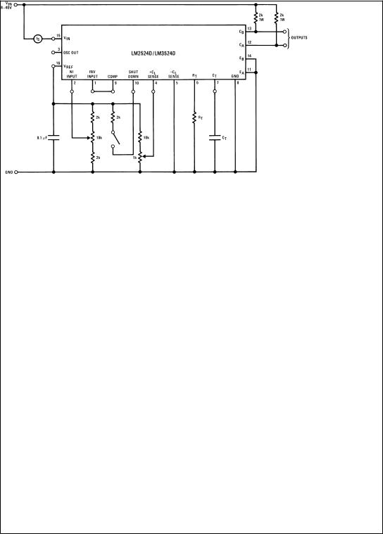
The LM3524D provides a stable on-board oscillator. Its frequency is set by an external resistor, RT and capacitor, CT. A graph of RT, CT vs oscillator frequency is shown is Figure 2. The oscillator's output provides the signals for triggering an internal flip-flop, which directs the PWM information to the outputs, and a blanking pulse to turn off both outputs during transitions to ensure that cross conduction does not occur. The width of the blanking pulse, or dead time, is controlled by the value of CT, as shown in Figure 3. The recommended values of RT are 1.8 kΩ to 100 kΩ, and for CT, 0.001 µF to 0.1 µF.
If two or more LM3524D's must be synchronized together, the easiest method is to interconnect all pin 3 terminals, tie all pin 7's (together) to a single CT, and leave all pin 6's open except one which is connected to a single RT. This method works well unless the LM3524D's are more than 6" apart.
A second synchronization method is appropriate for any circuit layout. One LM3524D, designated as master, must have its RTCT set for the correct period. The other slave LM3524D(s) should each have an RTCT set for a 10% longer period. All pin 3's must then be interconnected to allow the master to properly reset the slave units.
The oscillator may be synchronized to an external clock source by setting the internal free-running oscillator frequency 10% slower than the external clock and driving pin 3 with a pulse train (approx. 3V) from the clock. Pulse width should be greater than 50 ns to insure full synchronization.
DS008650-5
FIGURE 2.
DS008650-6
FIGURE 3.
ERROR AMPLIFIER
The error amplifier is a differential input, transconductance amplifier. Its gain, nominally 86 dB, is set by either feedback or output loading. This output loading can be done with either purely resistive or a combination of resistive and reactive components. A graph of the amplifier's gain vs output load resistance is shown in Figure 4.
DS008650-7
FIGURE 4.
The output of the amplifier, or input to the pulse width modulator, can be overridden easily as its output impedance is very high (ZO 5 MΩ). For this reason a DC voltage can be
www.national.com |
6 |
 Loading...