


LP2966IMMX-3030
NSC LP2966IMMX-3030, LP2966IMMX-2828, LP2966IMMX-1833, LP2966IMM-5050, LP2966IMM-3636 Datasheet
...
LP2966
Dual 150mA Ultra Low-Dropout Regulator
General Description
The LP2966 dual ultra low-dropout (LDO) regulator operates
from a +2.70V to +7.0V input supply. Each output delivers
150mAoverfulltemperaturerange.The IC operates with ex-
tremely low drop-out voltage and quiescent current, which
makes it very suitable for battery powered and portable ap-
plications. Each LDO in the LP2966 has independent shut-
down capability. The LP2966 provides low noise perfor-
mance with low ground pin current in an extremely small
MSOP-8 package (refer to package dimensions and connec-
tion diagram for more information on MSOP-8 package). A
wide range of preset voltage options are available for each
output. In addition to the voltage combinations listed in the
ordering information table, many more are available upon re-
quest with minimum orders. In all, 256 voltage combinations
are possible.
Key Specifications
Dropout Voltage: Varies linearly with load current. Typically
0.9 mV at 1mA load current and 135mV at 150mA load cur-
rent.
Ground Pin Current: Typically 300µA at 1mA load current
and 340µA at 100mA load current (with one shutdown pin
pulled low).
Shutdown Mode: Less than 1µA quiescent current when
both shutdown pins are pulled low.
Error Flag: Open drain output, goes low when the corre-
sponding output drops 10% below nominal.
Precision Output Voltage: Multiple output voltage options
available ranging from 1.8V to 5.0V with a guaranteed accu-
racy of
±
1% at room temperature.
Features
n Ultra low drop-out voltage
n Low ground pin current
n
<
1µA quiescent current in shutdown mode
n Independent shutdown of each LDO regulator
n Output voltage accuracy
±
1%
n Guaranteed 150mA output current at each output
n Low output noise
n Error Flags indicate status of each output
n Available in MSOP-8 surface mount packages
n Low output capacitor requirements (1µF)
n Operates with Low ESR ceramic capacitors in most
applications
n Over temperature/over current protection
n -40˚C to +125˚C junction temperature range
Applications
n Cellular and Wireless Applications
n Palmtop/Laptop Computer
n GPS systems
n Flat panel displays
n Post regulators
n USB applications
n Hand held equipment and multimeters
n Wireless data terminals
n Other battery powered applications
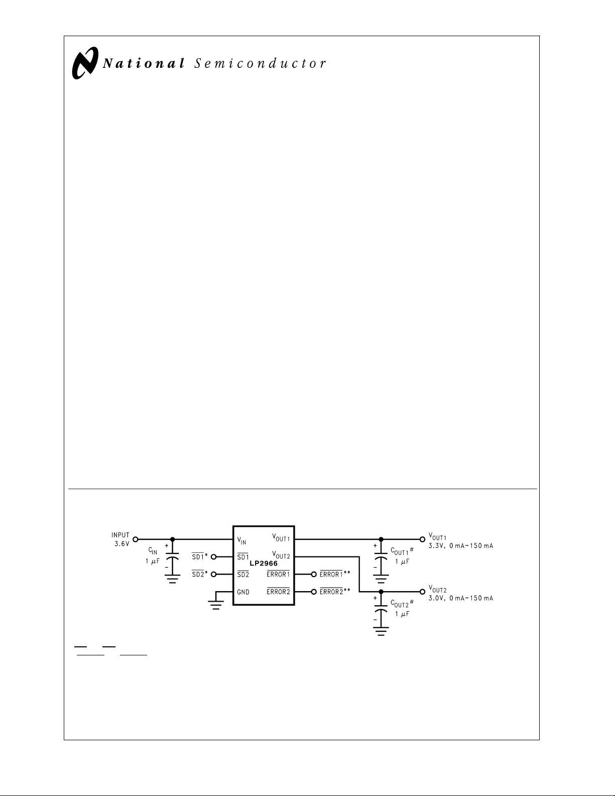
Typical Application Circuit
DS100850-30
*SD1 and SD2 must be actively terminated through a pull up resistor. Tie to V
IN
if not used.
**ERROR1 and ERROR2 are open drain outputs. These pins must be connected to ground if not used.
# Minimum output capacitance is 1µF to insure stability over full load current range. More capacitance improves superior dynamic performance and provides
additional stability margin.
April 2000
LP2966 Dual 150mA Ultra Low-Dropout Regulator
© 2000 National Semiconductor Corporation DS100850 www.national.com
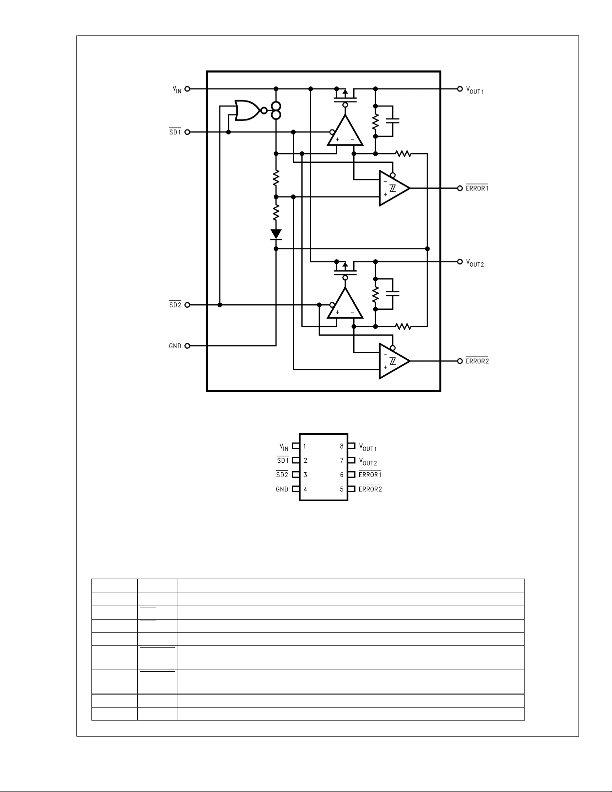
Block Diagram
Connection Diagram
Pin Description
Pin Name Function
1 VIN Input Supply pin
2 SD1
Active low shutdown pin for output 1
3 SD2
Active low shutdown pin for output 2
4 GND Ground
5 ERROR2
Error flag for output 2 - Normally high impedance, should be connected to ground if not
used.
6 ERROR1
Error flag for output 1 - Normally high impedance, should be connected to ground if not
used.
7 VOUT2 Output 2
8 VOUT1 Output 1
DS100850-31
DS100850-32
Top View
Mini SO-8 Package
8-Lead Small Outline Integrated Circuit (SOIC)
Package Code: MSOP-8
LP2966 Dual 150mA Ultra Low-Dropout Regulator
www.national.com 2
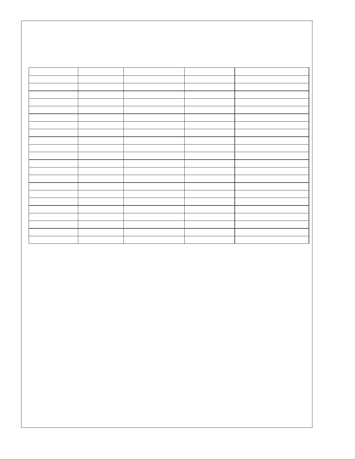
Ordering Information
The following voltage options and their combinations are possible.
5.0V, 4.0V, 3.8V, 3.6V, 3.3V, 3.2V, 3.1V, 3.0V, 2.9V, 2.8V, 2.7V, 2.6V, 2.5V, 2.4V, 2.0V and 1.8V
TABLE 1.
Output Voltage 1 Output Voltage 2 Order Number Package Marking Supplied As:
5.0 5.0 LP2966IMM-5050 LAFB 1000 units on tape and reel
5.0 5.0 LP2966IMMX-5050 LAFB 3500 units on tape and reel
3.6 3.6 LP2966IMM-3636 LAEB 1000 units on tape and reel
3.6 3.6 LP2966IMMX-3636 LAEB 3500 units on tape and reel
3.3 3.6 LP2966IMM-3336 LAHB 1000 units on tape and reel
3.3 3.6 LP2966IMMX-3336 LAHB 3500 units on tape and reel
3.3 3.3 LP2966IMM-3333 LADB 1000 units on tape and reel
3.3 3.3 LP2966IMMX-3333 LADB 3500 units on tape and reel
3.3 2.5 LP2966IMM-3325 LARB 1000 units on tape and reel
3.3 2.5 LP2966IMMX-3325 LARB 3500 units on tape and reel
3.0 3.0 LP2966IMM-3030 LACB 1000 units on tape and reel
3.0 3.0 LP2966IMMX-3030 LACB 3500 units on tape and reel
2.8 3.0 LP2966IMM-2830 LASB 1000 units on tape and reel
2.8 3.0 LP2966IMMX-2830 LASB 3500 units on tape and reel
2.8 2.8 LP2966IMM-2828 LABB 1000 units on tape and reel
2.8 2.8 LP2966IMMX-2828 LABB 3500 units on tape and reel
2.5 2.5 LP2966IMM-2525 LAAB 1000 units on tape and reel
2.5 2.5 LP2966IMMX-2525 LAAB 3500 units on tape and reel
1.8 3.3 LP2966IMM-1833 LCFB 1000 units on tape and reel
1.8 3.3 LP2966IMMX-1833 LCFB 3500 units on Tape and reel
1.8 1.8 LP2966IMM-1818 LA9B 1000 units on tape and reel
1.8 1.8 LP2966IMMX-1818 LA9B 3500 units on tape and reel
The voltage options and combinations shown in
Table 1
are available. For other custom voltage options or combinations
of voltage options, please contact your nearest National Semiconductor Sales Office.
LP2966 Dual 150mA Ultra Low-Dropout Regulator
www.national.com3
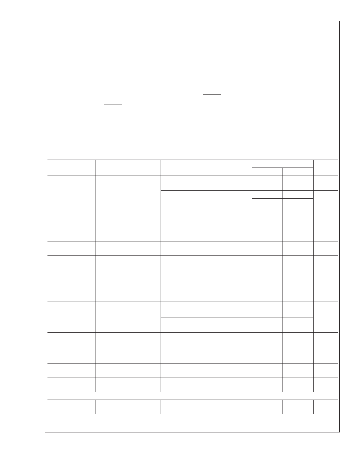
Absolute Maximum Ratings (Note 1)
If Military/Aerospace specified devices are required,
please contact the National Semiconductor Sales Office/
Distributors for availability and specifications.
Storage Temperature Range −65 to +150˚C
Lead Temp. (Soldering, 5 sec.) 260˚C
Power Dissipation (Note 2) Internally Limited
ESD Rating (Note 3) 2kV
Input Supply Voltage (Survival) −0.3V to 7.5V
Shutdown Input Voltage (Survival) −0.3V to (Vin + 0.3V)
Maximum Voltage for ERROR
Pins
10V
I
OUT
(Survival) Short Circuit
Protected
Output Voltage (Survival)(Note 6),
(Note 7)
−0.3V to (Vin + 0.3V)
Operating Ratings (Note 1)
Input Supply Voltage 2.7V to 7.0V
Shutdown Input Voltage −0.3V to (Vin + 0.3V)
Operating Junction
Temperature Range
−40˚C to +125˚C
Maximum Voltage for
ERROR pins
10V
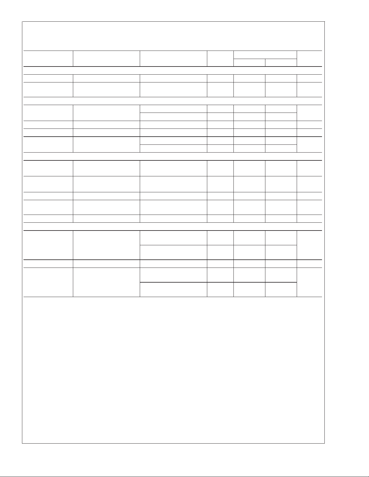
Electrical Characteristics
Limits in standard typeface are for T
j
= 25˚C, and limits in boldface type apply over the full operating junction temperature
range. Unless otherwise specified, V
IN
=V
O(NOM)
+ 1V, (Note 16), C
OUT
= 1µF, I
OUT
= 1mA, C
IN
= 1µF, V
SD1
=V
SD2
=V
IN
.
Symbol Parameter Conditions
Typ
(Note 4)
LP2966IMM (Note 5)
Unit
Min Max
V
o
(Note 13)
Output Voltage Tolerance V
OUT
+1V
<
V
IN
<
7.0V 0.0 −1 1
%V
NOM
-3 3
1mA
<
I
L
<
100mA 0.0 −1.5 1.5
%V
NOM
-3.5 3.5
∆V
O
/∆V
IN
(Note 8)
(Note 13)
Output Voltage Line
Regulation
0.1 mV/V
∆V
O
/∆I
OUT
Output Voltage Load
Regulation (Note 9)
1mA
<
I
L
<
100mA
(Note 9)
0.1 mV/mA
∆V
O2
/∆I
OUT1
Output Voltage Cross
Regulation (Note 10)
1mA
<
I
L1
<
100mA
(Note 10)
0.0004
mV/mA
V
IN
-V
OUT
Dropout Voltage
(Note 12)
I
L
= 1mA 0.9 2.0
3.0
I
L
= 100mA 90 130
mV
180
I
L
= 150mA 135 195
270
I
GND(1,0)
(Note 18) Ground Pin Current (One
LDO On)
I
L
= 1mA 300
µA
V
SD2
≤ 0.1V, V
SD1
=V
IN
I
L
= 100mA 340
V
SD2
≤ 0.1V, V
SD1
=V
IN
I
GND(1,1)
Ground Pin Current (Both
LDOs On)
I
L
= 1mA 340 450
µA
500
I
L
= 100mA 420 540
600
I
GND(0,0)
Ground Pin Current in
Shutdown Mode
V
SD1
=V
SD2
≤ 0.1V 0.006 0.3
10
µA
I
O(PK)
Peak Output Current (Note 2)
V
OUT
≥ V
OUT(NOM)
-5%
500 350
150
mA
Short Circuit Foldback Protection
I
FB
Short Circuit Foldback
Knee
(Note 2), (Note 14) 600 mA
LP2966 Dual 150mA Ultra Low-Dropout Regulator
www.national.com 4
Electrical Characteristics (Continued)
Limits in standard typeface are for T
j
= 25˚C, and limits in boldface type apply over the full operating junction temperature
range. Unless otherwise specified, V
IN
=V
O(NOM)
+ 1V, (Note 16), C
OUT
= 1µF, I
OUT
= 1mA, C
IN
= 1µF, V
SD1
=V
SD2
=V
IN
.
Symbol Parameter Conditions
Typ
(Note 4)
LP2966IMM (Note 5)
Unit
Min Max
Over Temperature Protection
Tsh(t) Shutdown Threshold 165 ˚C
Tsh(h) Thermal Shutdown
Hysteresis
25
˚C
Shutdown Input
V
SDT
Shutdown Threshold
(Note 15)
Output = Low 0 0.1
V
Output = High V
IN
V
IN
- 0.1
T
dOFF
Turn-off Delay (Note 17) I
L
= 100 mA 20 µsec
T
dON
Turn-on Delay (Note 17) I
L
= 100 mA 25 µsec
I
SD
SD Input Current V
SD
=V
IN
1
nA
V
SD
=0V 1
Error Flag Comparators
V
T
Threshold (output goes
high to low)
10 516%
(Note 11)
V
TH
Threshold Hysteresis 5 28%
(Note 11)
V
ERR(Sat)
Error Flag Saturation I
Fsink
= 100µA 0.015 0.1 V
I
EF(leak)
Error Flag Pin Leakage
Current
1nA
I
(EFsink)
Error Flag Pin Sink Current 1 mA
AC Parameters
PSRR Ripple Rejection V
IN
=V
OUT
+ 1V, f =
120Hz, V
OUT
= 3.3V
60
dB
V
IN
=V
OUT
+ 0.3V, f =
120Hz, V
OUT
= 3.3V
40
ρn(1/f) Output Noise Density f =120Hz 1 µV/
√
Hz
e
n
Output Noise Voltage (rms) BW = 10Hz − 100kHz,
C
OUT
= 10µF
150
µV(rms)
BW = 300Hz − 300kHz,
C
OUT
= 10µF
100
Note 1: Absolute maximum ratings indicate limits beyond which damage to the device may occur. Operating ratings indicate conditions for which the device is in-
tended to be functional, but do not guarantee specific performance limits. For guaranteed specifications and test conditions, see Electrical characteristics. The guar-
anteed specifications apply only for the test conditions listed. Some performance characteristics may degrade when the device is not operated under the listed test
conditions.
Note 2: At elevated temperatures, devices must be derated based on package thermal resistance. The device in the surface-mount package must be derated at θ
jA
= 235˚C/W, junction-to-ambient. Please refer to the applications section on maximum current capability for further information. The device has internal thermal pro-
tection.
Note 3: The human body model is a 100pF capacitor discharged through a 1.5kΩ resistor into each pin.
Note 4: : Typical numbers are at 25˚C and represent the most likely parametric norm.
Note 5: : Limits are 100% production tested at 25˚C. Limits over the operating temperature range are guaranteed through correlation using Statistical Quality Control
(SQC) methods. The limits are used to calculate National’s Averaging Outgoing Quality Level (AOQL).
Note 6: If used in a dual-supply system where the regulator load is returned to a negative supply, the LP2966 output must be diode-clamped to ground.
Note 7: The output PMOS structure contains a diode between the V
IN
and V
OUT
terminals that is normally reverse-biased. Reversing the polarity from V
IN
and V
OUT
will turn on this diode.
Note 8: Output voltage line regulation is defined as the change in output voltage from the nominal value due to change in input line voltage.
Note 9: Output voltage load regulation is defined as the change in output voltage from the nominal value when the load current changes from 1mAto 100mA.
Note 10: Output voltage cross regulation is defined as the percentage change in the output voltage from the nominal value at one output when the load current
changes from 1mAto full load in the other output. This is an important parameter in multiple output regulators. The specification for ∆V
O1
/∆I
OUT2
is equal to the speci-
fication for ∆V
O2
/∆I
OUT1
.
Note 11: Error Flag threshold and hysteresis are specified as the percentage below the regulated output voltage.
Note 12: Dropout voltage is defined as the input to output differential at which the output voltage drops 100mV below the nominal value. Drop-out voltage specifi-
cation applies only to output voltages greater than 2.7V.For output voltages below 2.7V, the drop-out voltage is nothing but the input to output differential, since the
minimum input voltage is 2.7V.
Note 13: Output voltage tolerance specification also includes the line regulation and load regulation.
LP2966 Dual 150mA Ultra Low-Dropout Regulator
www.national.com5
 Loading...