


LMC6684BIM
NSC LMC6684BIM, LMC6684AIM, LMC6682BIN, LMC6682BIM, LMC6682AIN Datasheet
...
LMC6681 Single/LMC6682 Dual/LMC6684 Quad
Low Voltage, Rail-To-Rail Input and Output CMOS
Amplifier with Powerdown
May 1995
LMC6681 Single/LMC6682 Dual/LMC6684 Quad Low Voltage, Rail-To-Rail Input and Output CMOS
Amplifier with Powerdown
General Description
The LMC6681/2/4 is a high performance operational amplifier which can operate over a wide range of supply voltages,
with guaranteed specifications at 1.8V, 2.2V, 3V, 5V, and
10V.
The LMC6681/2/4 provides an input common-mode voltage
range that exceeds both supplies. The rail-to-rail output
swing of the amplifier assures maximum dynamic signal
range. This rail-to-rail performance of the amplifier, combined with its high open-loop voltage gain makes it unique
among CMOS rail-to-rail amplifiers. The LMC6681/2/4 is an
excellent choice for circuits where the common-mode voltage range is a concern.
The LMC6681/2/4 has a powerdown mode which can be
controlled externally. In this powerdown mode, the supply
current decreases from 700 µA per amplifier to less than 1
µA per amplifier. The LMC6684 has two powerdown options.
Each of the powerdown pins disables two amplifiers.
The LMC6681/2/4 has been designed specifically to improve
system performance in low voltage applications. The amplifier’s 80 fA input current, 0.5 mV offset voltage, and 82 dB
CMRR maintain accuracy in battery-powered systems.
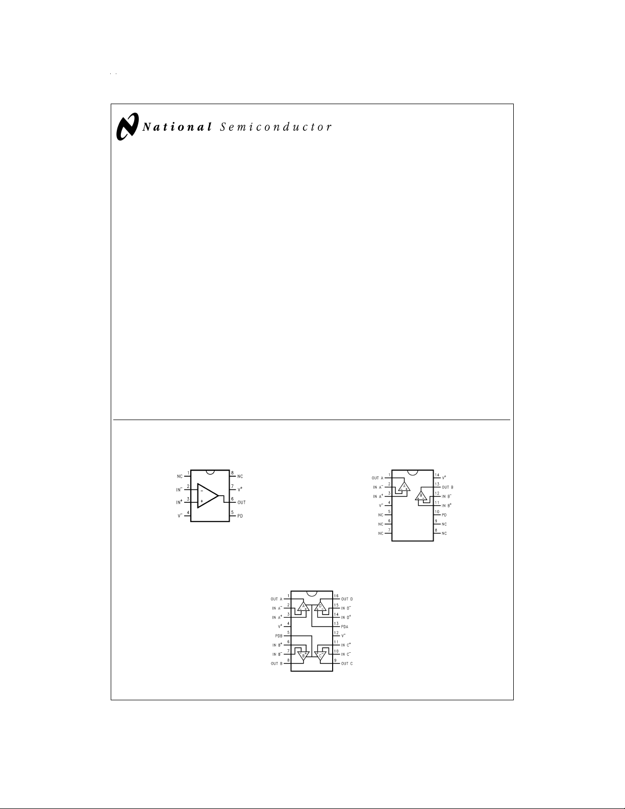
Connection Diagrams
8-Pin DIP/SO
Features
(Typical unless otherwise noted)
n Guaranteed Specs at 1.8V, 2.2V, 3V, 5V, 10V
n Rail-to-Rail Input Common-Mode Voltage Range
n Rail-to-Rail Output Swing
(within 10 mV of supply rail,
n Powerdown Mode I
(Guaranteed at V
n Ultra Low Input Current 80 fA
n High Voltage Gain (V
n Unity Gain Bandwidth 1.2 MHz
S OFF
=
1.8V, 2.2V, 3V, and 5V)
S
=
S
=
@
V
3V and R
S
≤ 1.5 µA/Amplifier
=
3V, R
10 kΩ): 120 dB
L
L
Applications
n Battery Operated Circuits
n Sensor Amplifiers
n Portable Communication Devices
n Medical Instrumentation
n Battery Monitoring Circuits
n Level Detectors, Sample-and-Hold Circuits
14-Pin DIP/SO
=
10 kΩ)
DS012042-1
Top View
Top View
16-Pin DIP/SO
DS012042-3
Top View
© 1999 National Semiconductor Corporation DS012042 www.national.com
DS012042-2
Ordering Information
Package Temperature Range NSC Transport
8-Pin Molded DIP LMC6681AIN, LMC6681BIN N08E Rails
8-Pin Small Outline LMC6681AIM, LMC6681BIM M08A Rails
14-Pin Molded DIP LMC6682AIN, LMC6682BIN N14A Rails
14-Pin Small Outline LMC6682AIM, LMC6682BIM M14A Rails
16-Pin Molded DIP LMC6684AIN, LMC6684BIN N16A Rails
16-Pin Small Outline LMC6684AIM, LMC6684BIM M16A Rails
Industrial, −40˚C to +85˚C Drawing Media
LMC6681AIMX, LMC6681B1MX M08A Tape and Reel
LMC6682AIMX, LMC6682BIMX M14A Tape and Reel
LMC6684AIMX, LMC6684BIMX M16A Tape and Reel
www.national.com 2
Absolute Maximum Ratings (Note 1)
If Military/Aerospace specified devices are required,
please contact the National Semiconductor Sales Office/
Distributors for availability and specifications.
ESD Tolerance (Note 2) 2 kV
±
Differential Input Voltage
Voltage at Input/Output Pin (V
Supply Voltage (V
+
− V−) 12V
Current at Input Pin (Note 11)
Current at Output Pin (Note 3)
Supply Voltage
+
) +0.3V, (V−) −0.3V
±
5mA
±
30 mA
Current at Power Supply Pin 35 mA
Lead Temp. (soldering, 10 sec.) 260˚C
Storage Temperature Range −65˚C to +150˚C
Junction Temperature (Note 4) 150˚C
3V DC Electrical Characteristics
Unless otherwise specified, all limits guaranteed for T
1MΩ.Boldface limits apply at the temperature extremes (Note 16).
J
=
25˚C, V
Operating Ratings (Note 1)
Supply Voltage 1.8V ≤ V
Junction Temperature Range
LMC6681AI, LMC6681BI −40˚C ≤ T
LMC6682AI, LMC6682BI −40˚C ≤ T
LMC6684AI, LMC6684BI −40˚C ≤ T
Thermal Resistance (θ
N Package, 8-pin Molded DIP 108˚C/W
M Package, 8-pin Surface Mount 172˚C/W
N Package, 14-pin Molded DIP 88˚C/W
M Package, 14-pin Surface Mount 126˚C/W
N Package, 16-pin Molded DIP 83˚C/W
M Package, 16-pin Surface Mount 114˚C/W
+
=
3.0V, V−=0V, V
)
JA
=
CM
+
=
V
V
O
/2, V
PD
=
0.6V and R
≤ 10V
S
≤ +85˚C
J
≤ +85˚C
J
≤ +85˚C
J
LMC6681AI LMC6681BI
LMC6682AI LMC6682BI
LMC6684AI LMC6684BI
Limit Limit
Units
Symbol Parameter Conditions
Typ
(Note 5)
(Note 6) (Note 6)
V
OS
Input Offset Voltage 0.5 1 3 mV
2.5 4.5 max
TCV
Input Offset Voltage 1.5 µV/˚C
OS
Average Drift
I
B
I
OS
R
IN
C
IN
Input Current (Note 12) 0.08 20 20 pA max
Input Offset Current (Note 12) 0.04 10 10 pA max
Input Resistance
>
1 Tera Ω
Input Capacitance 3 pF
CMRR Common Mode (Note 13) 82 70 65 dB
Rejection Ratio 65 62 min
PSRR Power Supply
Rejection Ratio V
V
CM
Input Common Mode CMRR>50 dB 3.23 3.18 3.18 V
±
1.5V ≤ VS≤±2.5V 82 70 65 dB
+
=
/2=V
V
O
CM
65 62 min
Voltage Range 3.00 3.00 min
−0.3 −0.18 −0.18 V
0.00 0.00 max
A
V
V
O
Large Signal
Voltage Gain
Output Swing R
=
R
600Ω (Notes 7, 12) 70 10 10 V/mV
L
=
R
10 kΩ (Notes 7, 12) 1000 12 12 V/mV
L
=
L
600Ω to V
+
/2 2.87 2.70 2.70 V
2.58 2.58 min
0.15 0.3 0.3 V
0.42 0.42 max
2kΩto V
+
/2 2.95 2.85 2.85 V
=
R
L
2.79 2.79 min
0.05 0.15 0.15 V
0.21 0.21 max
R
L
=
10 kΩ to V
+
/2 2.99 2.94 2.94 V
2.91 2.91 min
0.01 0.04 0.04 V
0.05 0.05 max
>
L
www.national.com3
3V DC Electrical Characteristics (Continued)
Unless otherwise specified, all limits guaranteed for T
1MΩ.Boldface limits apply at the temperature extremes (Note 16).
Symbol Parameter Conditions
I
SC
Output Short Sourcing, V
Circuit Current 6.7 6.7 min
Sinking, V
I
SON
Supply Current Single, LMC6681 0.7 1.13 1.13 mA
when Powered ON V
=
1.5V 1.36 1.36 max
CM
Dual, LMC6682 1.4 2.26 2.26 mA
=
V
1.5V 2.75 2.75 max
CM
Quad, LMC6684 2.8 4.52 4.52 mA
=
V
1.5V 5.42 5.42 max
I
S OFF
Supply Current Single, LMC6681 0.5 1.5 1.5 µA
when Powered OFF V
CM
=
2.3V 2.1 2.1 max
PD
Dual, LMC6682 0.5 1.5 1.5 µA
=
V
2.3V 2.1 2.1 max
PD
Quad, LMC6684 1.0 3.0. 3.0 µA
=
V
2.3V 4.2 4.2 max
PD
=
25˚C, V
J
=
0V 20 9.0 9.0 mA
O
=
3V 12 6.0 6.0 mA
O
+
=
3.0V, V−=0V, V
Typ
(Note 5)
+
=
=
V
CM
V
O
/2, V
=
PD
0.6V and R
LMC6681AI LMC6681BI
LMC6682AI LMC6682BI
LMC6684AI LMC6684BI
Limit Limit
(Note 6) (Note 6)
4.5 4.5 min
L
Units
>
www.national.com 4

1.8V and 2.2V DC Electrical Characteristics
Unless otherwise specified, all limits guaranteed for T
@
2.2V), V
(
=
@
1.8V) and R
0.3V (
PD
>
1MΩ.Boldface limits apply at the temperature extremes (Note 16).
L
=
25˚C, V+=1.8V and 2.2V, V−=0V, V
J
CM
+
=
=
V
V
O
/2, V
=
0.4V
PD
LMC6681AI LMC6681BI
Typ LMC6682AI LMC6682BI
Symbol Parameter Conditions (Note 5) LMC6684AI LMC6684BI Units
Limit Limit
(Note 6) (Note 6)
+
V
OS
Input Offset Voltage V
=
1.8V, V
+
=
V
2.2V, V
=
1.5V 0.5 3 10 mV max
CM
=
1.5V 0.5 2 6 mV
CM
3.8 7.8 max
+
TCV
Input Offset Voltage V
OS
=
2.2V 1.5 µV/˚C
Average Drift
+
I
B
I
OS
Input Current V
Input Offset Current V
CMRR Common Mode V
Rejection Ratio V
PSRR Power Supply
Rejection Ratio V
V
CM
Input Common Mode V
Voltage Range −0.15 0.0 0.0 V max
V
O
Output Swing V
=
2.2V (Note 12) 0.08 20 20 pA max
+
=
2.2V (Note 12) 0.04 10 10 pA max
+
=
2.2V (Note 13) 82 60 60 dB min
+
=
1.8V (Note 13) 82 50 50 dB min
±
1.1V ≤ VS≤±5V, 82 70 65 dB
+
=
/2=V
V
O
+
=
CMRR
+
=
V
CMRR
+
=
=
R
L
2.2V
>
1.8V
>
CM
40 dB
40 dB
2.38 2.2 2.2 V min
1.98 1.8 1.8 V min
−0.10 0.0 0.0 V max
2.2V 2.15 2.0 2.0 V
+
2kΩto V
/2 1.88 1.88 min
65 62 min
0.05 0.2 0.2 V
0.32 0.32 max
+
=
V
1.8V 1.75 1.6 1.6 V
=
R
2kΩto V
L
+
/2 1.44 1.44 min
0.05 0.2 0.2 V
0.32 0.32 max
I
SON
Supply Current Single, LMC6681 0.7 1.1 1.1 mA
when Powered ON V
=
1.5V 1.32 1.32 max
CM
Dual, LMC6682 1.4 2.2 2.2 mA
=
V
1.5V 2.7 2.7 max
CM
Quad, LMC6684 2.8 4.4 4.4 mA
=
V
1.5V 5.3 5.3 max
I
S OFF
Supply Current Single, LMC6681 0.5 1.5 1.5 µA
when Powered OFF V
CM
=
1.5V 2.7 2.7 max
PD
Dual, LMC6682 0.5 1.5 1.5 µA
=
V
1.5V 2.7 2.7 max
PD
Quad, LMC6684 1.0 3.0 3.0 µA
=
V
1.5V 5.4 5.4 max
PD
www.national.com5
5V DC Electrical Characteristics
Unless otherwise specified, all limits guaranteed for T
1MΩ.Boldface limits apply at the temperature extremes (Note 16).
=
J
25˚C, V
+
=
5.0V, V−=0V, V
+
=
=
V
CM
V
O
/2, V
=
PD
0.9V and R
LMC6681AI LMC6681BI
LMC6682AI LMC6682BI
LMC6684AI LMC6684BI
Limit Limit
Units
Symbol Parameter Conditions
Typ
(Note 5)
(Note 6) (Note 6)
V
OS
Input Offset Voltage V
=
1.5V 0.5 1 3 mV
CM
2.5 4.5 max
TCV
OS
Input Offset Voltage 1.5 µV/˚C
Average Drift
I
B
I
OS
R
IN
C
IN
Input Current (Note 12) 0.08 20 20 pA max
Input Offset Current (Note 12) 0.04 10 10 pA max
Input Resistance
>
1 Tera Ω
Input Capacitance 3 pF
CMRR Common Mode (Note 13) 82 70 65 dB
Rejection Ratio 65 62 min
PSRR Power Supply Rejection
Ratio V
V
CM
Input Common Mode CMRR>50 dB 5.3 5.18 5.18 V
±
1.5V ≤ VS≤±2.5V 82 70 65 dB
+
=
/2=V
V
O
CM
65 62 min
Voltage Range 5.00 5.00 min
−0.3 −0.18 −0.18 V
0.00 0.00 max
V
O
Output Swing R
=
L
2kΩto V
+
/2 4.9 4.85 4.85 V
4.58 4.58 min
0.05 0.2 0.2 V
0.28 0.28 max
I
SON
Supply Current Single, LMC6681 0.8 1.24 1.24 mA
when Powered ON V
=
1.5V 1.49 1.49 max
CM
Dual, LMC6682 1.5 2.48 2.48 mA
=
V
1.5V 3.00 3.00 max
CM
Quad, LMC6684 3.0 4.96 4.96 mA
=
V
1.5V 6.00 6.00 max
I
S OFF
Supply Current Single, LMC6681 0.5 1.5 1.5 µA
when Powered OFF V
CM
=
4.3V 2.1 2.1 max
PD
Dual, LMC6682 0.5 1.5 1.5 µA
=
V
4.3V 2.1 2.1 max
PD
Quad, LMC6684 1.0 3.0 3.0 µA
=
V
4.3V 4.2 4.2 max
PD
>
L
www.national.com 6
10V DC Electrical Characteristics
Unless otherwise specified, all limits guaranteed for T
>
1MΩ.Boldface limits apply at the temperature extremes (Note 16).
=
J
25˚C, V
+
=
10.0V, V−=0V, V
+
=
=
V
CM
V
O
/2, V
PD
=
1.2V and R
LMC6681AI LMC6681BI
LMC6682AI LMC6682BI
LMC6684AI LMC6684BI
Limit Limit
Units
Symbol Parameter Conditions
Typ
(Note 5)
(Note 6) (Note 6)
V
OS
Input Offset Voltage V
=
1.5V 0.5 1.5 3.5 mV
CM
3.0 5.0 max
TCV
Input Offset Voltage 1.5 µV/˚C
OS
Average Drift
I
B
I
OS
R
IN
C
IN
Input Current (Note 12) 0.08 20 20 pA max
Input Offset Current (Note 12) 0.04 10 10 pA max
Input Resistance
>
1 Tera Ω
Input Capacitance 3 pF
CMRR Common Mode (Note 13) 82 65 65 dB
Rejection Ratio 62 62 min
PSRR Positive Power Supply
Rejection Ratio V
V
CM
Input Common Mode CMRR>50 dB 10.30 10.18 10.18 V
±
1.1V ≤ VS≤±5V 82 70 65 dB
+
=
/2 65 62 min
V
O
Voltage Range 10.00 10.00 min
−0.30 −0.18 −0.18 V
0.00 0.00 max
V
O
Output Swing R
=
L
2kΩto V
+
/2 9.93 9.7 9.7 V
9.58 9.58 min
0.08 0.3 0.3 V
0.42 0.42 max
A
V
Large Signal R
=
L
2kΩto V
+
/2 Sourcing 89 25 25 V/mV
Voltage Gain (Note 12) Sinking 224 25 25 V/mV
I
SC
Output Short Circuit Sourcing, V
=
0V 65 30 30 mA
O
Current (Note 14) 22 22 min
Sinking, V
=
10V 70 30 30 mA
O
(Note 14) 22 22 min
I
SON
Supply Current Single, LMC6681 0.9 1.50 1.50 mA
when Powered ON V
=
1.5V 1.8 1.8 max
CM
Dual, LMC6682 1.6 3.00 3.00 mA
=
V
1.5V 3.6 3.6 max
CM
Quad, LMC6684 3.2 6.00 6.00 mA
=
V
1.5V 7.2 7.2 max
I
S OFF
Supply Current Single, LMC6681 0.5 5 5 µA
when Powered OFF V
CM
=
9.3V 77max
PD
Dual, LMC6682 0.5 5 5 µA
=
V
9.3V 77max
PD
Quad, LMC6684 1.0 10 10 µA
=
V
9.3V 14 14 max
PD
L
www.national.com7

Powerdown DC Threshold Characteristics
Boldface limits apply at the temperature extremes (Note 16).
Symbol Parameter Conditions
+
V
V
PD, IL
PD, IH
Powerdown Voltage Input Low (Device V
Powered ON; Amplifier meets all V
specs in the datasheet tables) V
Powerdown Voltage Input High (Device V
Powered OFF; Refer to DC Electrical V
Characteristics for I
specs) V
S OFF
=
2.2V 0.4 V
−
=
0V 0.25
+
=
3V 0.6 V
−
=
V
0V 0.45
+
=
V
5V 0.9 V
−
=
V
0V 0.75
+
=
V
10V 1.2 V
−
=
V
0V 1.05
+
=
2.2V 1.5 V
−
=
0V 1.65
+
=
3V 2.3 V
−
=
V
0V 2.45
+
=
V
5V 4.3 V
−
=
V
0V 4.45
+
=
V
10V 9.3 V
−
=
V
0V 9.45
LMC6681AI, LMC6681BI
LMC6682AI, LMC6682BI
LMC6684AI, LMC6684BI
Min Typ Max
Units
www.national.com 8
 Loading...