


M30803MC-XXXGP
Table of contents
 Loading...
Mitsubishi M30803MC-XXXGP, M30803MC-XXXFP, M30803FGGP, M30803FGFP, M30800MC-XXXGP Datasheet
...
Under
development
Description
Preliminary Specifications REV.D
Specifications in this manual are tentative and subject to change.
M16C/80 (100-pin version) group
SINGLE-CHIP 16-BIT CMOS MICROCOMPUTER
Mitsubishi microcomputers
Description
The M16C/80 (100-pin version) group of single-chip microcomputers are built using the high-performance
silicon gate CMOS process using a M16C/60 Series CPU core and are packaged in a 100-pin plastic
molded QFP. These single-chip microcomputers operate using sophisticated instructions featuring a high
level of instruction efficiency. With 16M bytes of address space, they are capable of executing instructions
at high speed. They also feature a built-in multiplier and DMAC, making them ideal for controlling office,
communications, industrial equipment, and other high-speed processing applications.
The M16C/80 (100-pin version) group includes a wide range of products with different internal memory
types and sizes and various package types.
Features
• Memory capacity..................................ROM (See ROM expansion figure.)
RAM 10/20 Kbytes
• Shortest instruction execution time......50ns (f(XIN)=20MHz)
• Supply voltage .....................................4.0 to 5.5V (f(XIN)=20MHz) Mask ROM and flash memory version
2.7 to 5.5V (f(XIN)=10MHz) Mask ROM and flash memory version
• Low power consumption ......................45mA (M30800MC-XXXFP)
• Interrupts..............................................29 internal and 8 external interrupt sources, 5 software
interrupt sources; 7 levels (including key input interrupt)
• Multifunction 16-bit timer......................5 output timers + 6 input timers
• Serial I/O..............................................5 channels
• DMAC ..................................................4 channels (trigger: 31 sources)
• DRAMC................................................Used for EDO, FP, CAS before RAS refresh, self-refresh
• A-D converter.......................................10 bits X 8 channels (Expandable up to 10 channels)
• D-A converter.......................................8 bits X 2 channels
• CRC calculation circuit.........................1 circuit
• X-Y converter.......................................1 circuit
• Watchdog timer....................................1 line
• Programmable I/O ...............................87 lines
• Input port..............................................
1 line (P85 shared with NMI pin)
• Memory expansion ..............................Available (16M bytes)
• Chip select output ................................4 lines
• Clock generating circuit .......................2 built-in clock generation circuits
(built-in feedback resistance, and external ceramic or quartz oscillator)
for UART or clock synchronous
Specifications written in this
manual are believed to be accurate, but are not guaranteed
_______
to be entirely free of error.
Specifications in this manual
may be changed for functional
or performance improvements.
Please make sure your manual
is the latest edition.
Applications
Audio, cameras, office equipment, communications equipment, portable equipment, etc.
------Table of Contents------
CPU ..............................................................11
Reset.............................................................16
Processor Mode............................................24
Clock Generating Circuit ...............................40
Protection......................................................52
Interrupts.......................................................53
Watchdog Timer............................................75
DMAC ...........................................................77
Timer.............................................................88
Serial I/O .....................................................120
A-D Converter .............................................162
D-A Converter .............................................172
CRC Calculation Circuit .............................. 174
X-Y converter ..............................................176
DRAM controller..........................................179
Programmable I/O Ports .............................186
Usage Precaution .......................................201
Electric characteristics ................................208
Flash memory version.................................255
1

Under
development
Description
Specifications in this manual are tentative and subject to change.
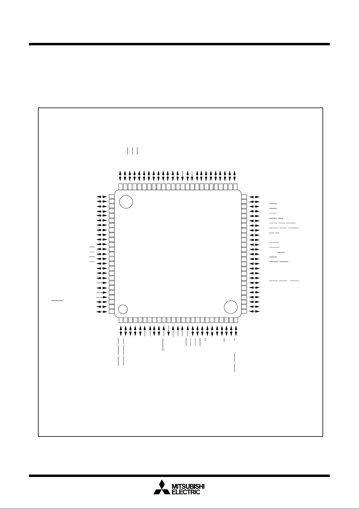
Pin Configuration
Figures 1.1.1 and 1.1.2 show the pin configurations (top view).
PIN CONFIGURATION (top view)
)
Preliminary Specifications REV.D
)
2
(/D
2
/A
2
P2
)
3
(/D
3
/A
3
P2
)
4
(/D
4
/A
4
P2
)
5
(/D
5
/A
5
P2
)
6
(/D
6
/A
6
P2
7
(/D
7
/A
7
P2
)
)
0
1
/INT5
/INT4
/INT3
(/D
(/D
8
9
10
11
/D
/D
/D
/D
0
1
2
3
P1
P1
P1
P1
15
14
13
12
/D
4
P1
0
1
/A
/D
/A
/D
/D
0
7
1
6
5
P2
P1
P2
P1
P1
)
8
(MA0)(/D
8
/A
0
P3
Vss
)
9
(MA1)(/D
9
/A
1
Vcc
P3
)
)
)
10
11
12
(MA2)(/D
(MA3)(/D
(MA4)(/D
10
11
12
/A
/A
/A
2
3
4
P3
P3
P3
Mitsubishi microcomputers
M16C/80 (100-pin version) group
SINGLE-CHIP 16-BIT CMOS MICROCOMPUTER
)
)
)
15
14
13
(MA7)(/D
(MA6)(/D
(MA8)
(MA9)
(MA10)
(MA5)(/D
15
14
13
/A
/A
/A
7
6
5
P3
P3
P3
(MA11)
16
17
18
19
/A
/A
/A
/A
0
1
2
3
P4
P4
P4
P4
P107/AN7/KI
P106/AN6/KI
P105/AN5/KI
P104/AN4/KI
P97/AD
/SCL4/STxD
P07/D
P06/D
P05/D
P04/D
P03/D
P02/D
P01/D
P00/D
P103/AN
P102/AN
P101/AN
AV
P100/AN
V
REF
AVcc
TRG/RXD4
515253545556575859606162636465666768697071727374757677787980
7
81
6
82
5
83
4
84
3
85
2
86
1
87
0
88
3
89
2
90
1
91
0
92
3
93
2
94
1
SS
95
96
0
97
98
99
00
1
4
1 2 3 4 5 6 7 8 9101112131415161718192021222324252627282930
4
4
4
/SS
4
/SRxD
4
/RTS
4
/SDA
/ANEX0/CLK
4
5
D
/CTS
X
P9
IN
/TB4
1
/ANEX1/T
/DA
6
4
P9
P9
M30800-XXXFP
3
3
3
3
/SS
3
/RTS
3
/CTS
IN
/TB3
0
/DA
3
P9
/STxD
/SRxD
3
3
/SCL
/SDA
3
3
D
D
X
X
/R
/T
IN
IN
/TB1
/TB2
1
2
P9
P9
/CLK
IN
/TB0
0
P9
BYTE
CNVss
CIN
/X
7
P8
COUT
/X
6
P8
OUT
X
RESET
IN
SS
X
V
1
0
2
CC
V
/NMI
/INT
/INT
5
3
4
P8
P8
P8
/INT
2
P8
/U
IN
/TA4
1
P8
/U
OUT
/TA4
0
P8
IN
/TA3
7
P7
OUT
/TA3
6
P7
/W
IN
/TA2
5
P7
/W
OUT
/TA2
4
P7
/V
IN
/TA1
2
/RTS
2
/CTS
3
P7
/V
OUT
/TA1
2
/CLK
2
P7
(Note)
IN
/TB5
IN
/TA0
2
/SCL
2
/RxD
1
P7
(Note)
OUT
/TA0
2
/SDA
2
D
X
/T
0
P7
P44/CS3/A20(MA12)
50
P45/CS2/A
49
48
P46/CS1/A
47
P47/CS0/A
46
P50/WRL/WR/CASL
45
P51/WRH/BHE/CASH
44
P52/RD/DW
43
P53/BCLK/ALE/CLK
42
P54/HLDA/ALE
41
P55/HOLD
40
P56/ALE/RAS
39
P57/RDY
38
P60/CTS0/RTS
37
P61/CLK
36
P62/RxD
35
34
33
32
31
3/TXD0
P6
P64/CTS1/RTS1/CTS0/CLKS
P65/CLK
P66/RxD
P67/TXD
21
22
23
OUT
0
0
0
1
1
1
1
Figure 1.1.1. Pin configuration (top view)
2
Note: This port is N-channel open drain output.
Package: 100P6S-A
Under
development
Description
PIN CONFIGURATION (top view)
P97/AD
TRG/RXD4
P96/ANEX1/TXD4/SDA4/SRxD
Preliminary Specifications REV.D
Specifications in this manual are tentative and subject to change.
)
)
)
10
P12/D
P11/D
P10/D
P07/D
P06/D
P05/D
P04/D
P03/D
P02/D
P01/D
P00/D
P107/AN7/KI
P106/AN6/KI
P105/AN5/KI
P104/AN4/KI
P103/AN
P102/AN
P101/AN
AV
P100/AN
V
AVcc
/SCL4/STxD
P95/ANEX0/CLK
REF
)
8
3
4
5
)
)
0
/INT
11
12
13
/D
/D
/D
3
4
5
P1
P1
P1
10
SS
76
9
77
8
78
79
7
6
80
5
81
4
82
83
3
2
84
1
85
0
86
3
87
2
88
1
89
0
90
3
91
2
92
93
1
94
95
0
96
97
98
4
99
4
00
1
4
1 2 3 4 5 6 7 8 910111213141516171819202122232425
1
/INT
/INT
(/D
(/D
0
14
15
1
/A
/A
/D
/D
0
1
6
7
P2
P2
P1
P1
M30800-XXXGP
)
2
(/D
2
/A
2
P2
)
3
(/D
3
/A
3
P2
)
4
(/D
4
/A
4
P2
)
5
(/D
5
/A
5
P2
)
6
(/D
6
/A
6
P2
)
7
(/D
7
/A
7
P2
(MA0)(/D
8
/A
0
P3
Vss
9
(MA1)(/D
9
/A
1
Vcc
P3
11
(MA2)(/D
(MA3)(/D
10
11
/A
/A
2
3
P3
P3
Mitsubishi microcomputers
M16C/80 (100-pin version) group
SINGLE-CHIP 16-BIT CMOS MICROCOMPUTER
)
)
)
)
14
12
13
15
(MA6)(/D
(MA8)
(MA7)(/D
14
15
/A
/A
6
7
P3
P3
16
/A
0
P4
51525354555657585960616263646566676869707172737475
(MA9)
17
/A
1
P4
50
49
48
47
46
45
44
43
42
41
40
39
38
37
36
35
34
33
32
31
30
29
28
27
26
P42/A18(MA10)
P4
3/A19
(MA11)
P44/CS3/A20(MA12)
P45/CS2/A
P46/CS1/A
P47/CS0/A
21
22
23
P50/WRL/WR/CASL
P51/WRH/BHE/CASH
P52/RD/W
P53/BCLK/ALE/CLK
P54/HLDA/ALE
P55/HOLD
P56/ALE/RAS
P57/RDY
P60/CTS0/RTS
P61/CLK
0
P62/RxD
0
P63/TXD
0
P64/CTS1/RTS1/CTS0/CLKS
P65/CLK
1
P66/RxD
1
P67/TXD
1
P70/TXD2/SDA2/TA0
P7
1
/RxD2/SCL2/TA0IN/TB5
P72/CLK2/TA1
0
OUT
OUT
OUT
(Note)
/V
(MA4)(/D
(MA5)(/D
12
13
/A
/A
4
5
P3
P3
IN
1
(Note)
3
3
3
4
/SS
4
/RTS
4
/CTS
IN
/TB4
1
/DA
4
P9
/SS
3
/RTS
3
/CTS
IN
/TB3
0
/DA
3
P9
/STxD
/SRxD
3
3
/SCL
/SDA
3
3
D
D
X
X
/R
/T
IN
IN
/TB1
/TB2
1
2
P9
P9
3
/CLK
IN
/TB0
0
P9
BYTE
CNVss
Figure 1.1.2. Pin configuration (top view)
CIN
/X
7
P8
COUT
/X
6
P8
OUT
X
RESET
IN
SS
CC
X
V
V
/NMI
/INT
/INT
5
3
4
P8
P8
P8
/INT
2
P8
/U
IN
/TA4
1
P8
/U
OUT
/TA4
0
P8
IN
/TA3
7
P7
OUT
/TA3
6
P7
/W
IN
/TA2
5
P7
/W
OUT
/TA2
4
P7
/V
IN
/TA1
2
/RTS
2
/CTS
3
P7
0
1
2
Note: This port is N-channel open drain output.
Package: 100P6Q-A
3
Under
A
A
A
development
Description
Specifications in this manual are tentative and subject to change.
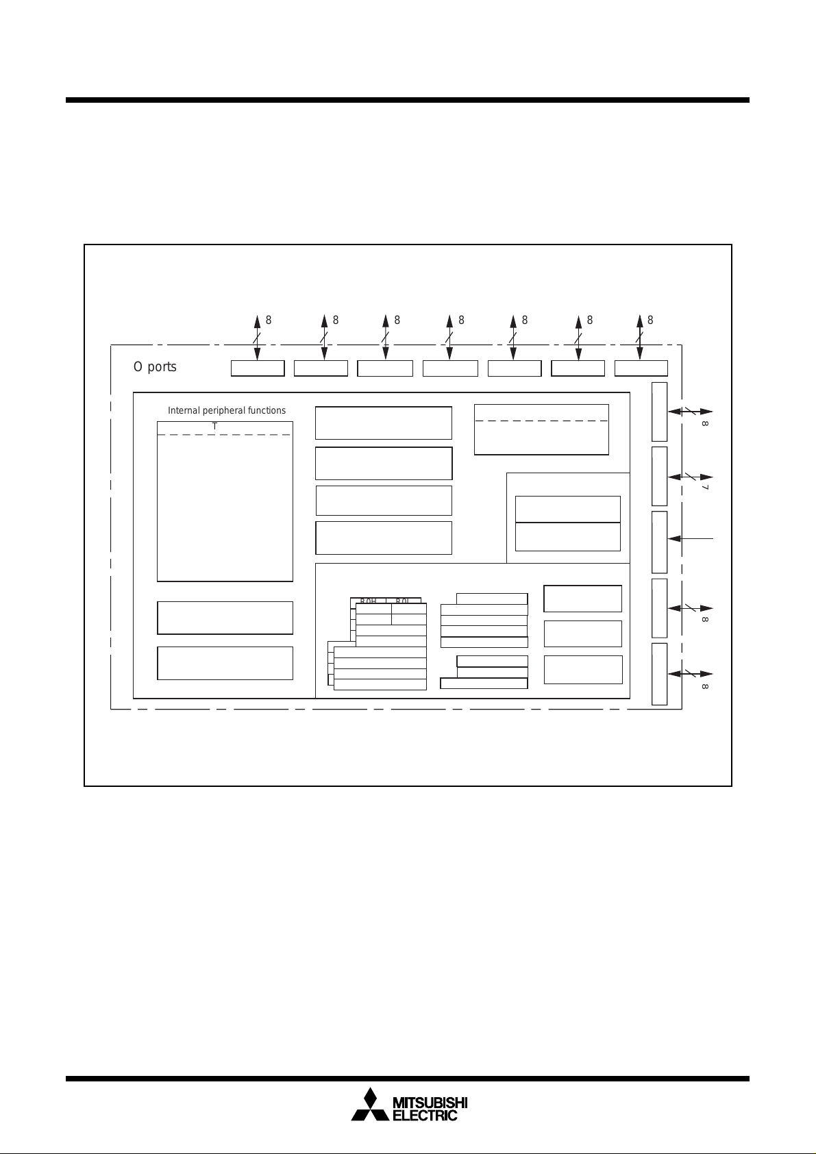
Block Diagram
Figure 1.1.3 is a block diagram of the M16C/80 (100-pin version) group.
Block diagram of the M30800MC-XXXGP
8888888
Preliminary Specifications REV.D
Mitsubishi microcomputers
M16C/80 (100-pin version) group
SINGLE-CHIP 16-BIT CMOS MICROCOMPUTER
I/O ports
Port P0
Internal peripheral functions
Timer
Port P1
Expandable up to 10 channels)
Timer TA0 (16 bits)
Timer TA1 (16 bits)
UART /clock synchronous SI/O
Timer TA2 (16 bits)
Timer TA3 (16 bits)
Timer TA4 (16 bits)
Timer TB0 (16 bits)
Timer TB1 (16 bits)
Timer TB2 (16 bits)
Timer TB3 (16 bits)
CRC arithmetic circuit (CCITT)
(Polynomial : X +X +X +1)
Timer TB4 (16 bits)
Timer TB5 (16 bits)
Watchdog timer
(15 bits)
D-A converter
(8 bits X 2 channels)
Note 1: ROM size depends on MCU type.
Note 2: RAM size depends on MCU type.
Port P2
A-D converter
(10 bits X 8 channels
(8 bits X 5 channels)
X-Y converter
(16 bits X 16 bits)
Port P3
System clock generator
1216 5
M16C/80 series 16-bit CPU core
Registers
R0LR0H
R0H R0L
R1H R1L
R1H R1L
R2
R2
R3
A0
A1
FB
SB
FLG
INTB
ISP
USP
PC
SVF
SVP
VCT
Port P4
XCIN - XCOUT
Port P5
XIN - XOUT
Memory
AAAAAA
AAAAAA
AAAAAA
ROM
(Note 1)
RAM
(Note 2)
DRAM
controller
DRAM
controller
Multiplier
Port P6
Port P7
8
Port P8
7
Port P8
5
Port P9
8
Port P10
8
Figure 1.1.3. Block diagram of M30800MC-XXXFP
4
Under
development
Description
Preliminary Specifications REV.D
Specifications in this manual are tentative and subject to change.
M16C/80 (100-pin version) group
SINGLE-CHIP 16-BIT CMOS MICROCOMPUTER
Mitsubishi microcomputers
Performance Outline
Table 1.1.1 is a performance outline of M16C/80 (100-pin version) group.
Table 1.1.1. Performance outline of M16C/80 (100-pin version) group
Item Performance
Number of basic instructions 106 instructions
Shortest instruction execution time 50ns(f(XIN)=20MHz)
Memory See ROM expansion figure.
capacity 10/20 K bytes
I/O port 8 bits x 10, 7 bits x 1
Input port 1 bit x 1
Multifunction 16 bits x 5
timer 16 bits x 6
Serial I/O (UART or clock synchronous) x 5
A-D converter 10 bits x (8 + 2) channels
D-A converter 8 bits x 2
DMAC 4 channels
DRAM controller CAS before RAS refresh, self-refresh, EDO, FP
CRC calculation circuit CRC-CCITT
X-Y converter 16 bits X 16 bits
Watchdog timer 15 bits x 1 (with prescaler)
Interrupt 29 internal and 8 external sources, 5 software sources, 7
Clock generating circuit 2 built-in clock generation circuits
Supply voltage 4. 2 to 5.5 V (f (XIN)=20MHz) Mask ROM and flash
Power consumption 45mA (f(XIN) = 20MHz without software wait,Vcc=5V)
I/O 5V
characteristics 5mA
Memory expansion Available (up to 16M bytes)
Operating ambient temperature –40 to 85oC
Device configuration CMOS high performance silicon gate
Package 100-pin plastic mold QFP
ROM
RAM
P0 to P10 (except P85)
P85
TA0, TA1, TA2, TA3,TA4
TB0, TB1, TB2, TB3, TB4, TB5
UART0, UART1, UART2,
UART3, UART4
levels
(built-in feedback resistance, and external ceramic or
quartz oscillator)
memory version
2.7 to 5.5V (f(XIN)=10MHz) Mask ROM and flash
memory version
Mask ROM 128 Kbytes version
I/O withstand voltage
Output current
5
Under
development
Description
Specifications in this manual are tentative and subject to change.
M16C/80 (100-pin version) group
SINGLE-CHIP 16-BIT CMOS MICROCOMPUTER
Mitsubishi plans to release the following products in the M16C/80 (100-pin version) group:
(1) Support for mask ROM version, external ROM version and flash memory version
(2) ROM capacity
(3) Package
100P6S-A : Plastic molded QFP (mask ROM version and flash memory version)
100P6Q-A : Plastic molded QFP (mask ROM version and flash memory version)
ROM Size
(Byte)
External
ROM
Preliminary Specifications REV.D
256K
128K
96K
80K
M30803MG-XXXFP/GP
M30800MC-XXXFP/GP
M30803FGFP/GP
M30800FCFP/GP
Mitsubishi microcomputers
64K
32K
Mask ROM version
Flash memory
version
External ROM version
Figure 1.1.4. ROM expansion
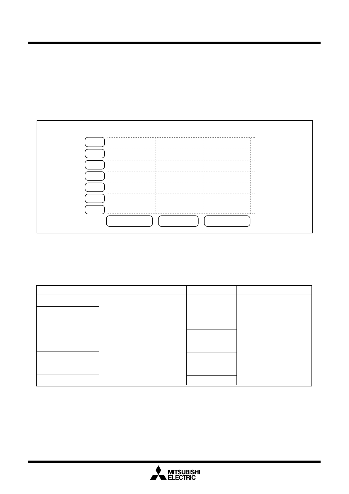
The M16C/80 (100-pin version) group products currently supported are listed in Table 1.1.2.
Table 1.1.2. M16C/80 (100-pin version) group
RAM capacityROM capacity Package type RemarksType No
M30800MC-XXXFP 128K byte s
M30800MC-XXXGP
M30803MG-XXXFP 256K bytes
M30803MG-XXXGP
M30800FCFP
M30800FCGP
M30803FGFP
M30803FGGP
:Under development
**
**
**
**
**
10K bytes 100P6S-A
100P6Q-A
20K bytes
100P6S-A
100P6Q-A
10K bytes128 K by t es
100P6S-A
100P6Q-A
20K bytes256 K by t es
100P6S-A
100P6Q-A
Mask ROM version
Flash memory version
As of June, 2000
6
Under
development
Description
Type No. M 3 0 8 0 0 M C – X X X F P
Preliminary Specifications REV.D
Specifications in this manual are tentative and subject to change.
Package type:
FP : Package 100P6S-A
GP : Package 100P6Q-A
ROM No.
Omitted for blank external ROM version
and flash memory version
ROM capacity:
C : 128K bytes
G : 256K bytes
Memory type:
M : Mask ROM version
S : External ROM version
F : Flash memory version
Mitsubishi microcomputers
M16C/80 (100-pin version) group
SINGLE-CHIP 16-BIT CMOS MICROCOMPUTER
Figure 1.1.5. Type No., memory size, and package
Shows RAM capacity, pin count, etc
(The value itself has no specific meaning)
M16C/80 Group
M16C Family
7
Under
development
Pin Description
Specifications in this manual are tentative and subject to change.
Pin Description
Pin name
VCC, V
SS
CNV
SS
Preliminary Specifications REV.D
Signal name
Power supply
input
CNV
SS
I/O type
Input
Mitsubishi microcomputers
M16C/80 (100-pin version) group
SINGLE-CHIP 16-BIT CMOS MICROCOMPUTER
Function
CC
Supply 4.2 to 5.5 V to the V
This pin switches between processor modes. Connect it to the V
when operating in single-chip or memory expansion mode after reset.
CC
Connect it to the V
when in microprocessor mode after reset.
pin. Supply 0 V to the VSS pin.
SS
RESET
X
IN
X
OUT
BYTE
AV
CC
AV
SS
V
REF
P00 to P0
7
Reset input
Clock input
Clock output
External data
bus width
select input
Analog power
supply input
Analog power
supply input
Reference
voltage input
I/O port P0
Input
Input
Output
Input
Input
Input/output
A “L” on this input resets the microcomputer.
These pins are provided for the main clock generating circuit. Connect
a ceramic resonator or crystal between the X
use an externally derived clock, input it to the X
X
OUT
pin open.
IN
and the X
IN
OUT
pin and leave the
pins. To
This pin selects the width of an external data bus. A 16-bit width is
selected when this input is “L”; an 8-bit width is selected when this
input is “H”. This input must be fixed to either “H” or “L”. When
not using the external bus,connect this pin to V
SS
.
This pin is a power supply input for the A-D converter. Connect this
pin to V
CC
.
This pin is a power supply input for the A-D converter. Connect this
pin to V
SS
.
This pin is a reference voltage input for the A-D converter.
This is an 8-bit CMOS I/O port. It has an input/output port direction
register that allows the user to set each pin for input or output
individually. When set for input in single chip mode, the user can
specify in units of four bits via software whether or not they are tied to a
pull-up resistance. In memory expansion and microprocessor mode,
an built-in pull-up resistance cannot be used. However, it is possible to
select pull-up resistance presence to the usable port as I/O port by
setting.
D0 to D
7
P10 to P1
D8 to D
P20 to P2
A0 to A
7
15
7
7
A0/D0 to
7/D7
A
P30 to P3
A8 to A
7
15
A8/D8 to
15/D15
A
MA0 to MA7
I/O port P1
I/O port P2
I/O port P3
Input/output
Input/output
Input/output
Input/output
Output
Input/output
Input/output
Output
Input/output
Output
When set as a separate bus, these pins input and output data (D
This is an 8-bit I/O port equivalent to P0. P1
5
to P17 also function as
0–D7
external interrupt pins as selected by software.
When set as a separate bus, these pins input and output data
(D8–D15).
This is an 8-bit I/O port equivalent to P0.
0–A7
These pins output 8 low-order address bits (A
If a multiplexed bus is set, these pins input and output data (D
0–A7
output 8 low-order address bits (A
) separated in time by
).
0–D7
) and
multiplexing.
This is an 8-bit I/O port equivalent to P0.
These pins output 8 middle-order address bits (A
8–A15
).
If the external bus is set as a 16-bit wide multiplexed bus, these pins
8–D15
input and output data (D
(A
8–A15
) separated in time by multiplexing.
) and output 8 middle-order address bits
If accessing to DRAM area, these pins output row address and column
address separated in time by multiplexing.
).
8
Under
development
Pin Description
Specifications in this manual are tentative and subject to change.
Pin Description
Preliminary Specifications REV.D
P40 to P4
A16 to A22,
A
23
CS
MA8 to MA12
P5
0
to CS
0
to P5
7
3
7
Signal name FunctionPin name I/O type
I/O port P4 This is an 8-bit I/O port equivalent to P0.Input/output
Output
Output
Output
I/O port P5 Input/output
Mitsubishi microcomputers
M16C/80 (100-pin version) group
SINGLE-CHIP 16-BIT CMOS MICROCOMPUTER
These pins output 8 high-order address bits (A
23
address bit (A
) outputs inversely.
These pins output CS0–CS3 signals. CS0–CS3 are chip select signals
used to specify an access space.
If accessing to DRAM area, these pins output data separated in time by
multiplexing.
This is an 8-bit I/O port equivalent to P0. P53 in this port outputs a
divide-by-8 or divide-by-32 clock of X
CIN
frequency as X
as selected by software.
IN
16–A22
, A23). Highest
or a clock of the same
WRL / WR,
WRH / BHE,
RD,
BCLK,
HLDA,
HOLD,
ALE,
RDY
DW,
CASL,
CASH,
RAS
P60 to P6
7
P70 to P77
I/O port P6
I/O port P7
Output
Output
Output
Output
Output
Input
Output
Input
Output
Output
Output
Output
Input/output
Input/output
Output WRL, WRH (WR and BHE), RD, BCLK, HLDA, and ALE
signals. WRL and WRH, and BHE and WR can be switched using
software control.
WRL, WRH, and RD selected
With a 16-bit external data bus, data is written to even addresses
when the WRL signal is “L” and to the odd addresses when the WRH
signal is “L”. Data is read when RD is “L”.
WR, BHE, and RD selected
Data is written when WR is “L”. Data is read when RD is “L”. Odd
addresses are accessed when BHE is “L”. Use this mode when using
an 8-bit external data bus.
While the input level at the HOLD pin is “L”, the microcomputer is
placed in the hold state. While in the hold state, HLDA outputs a “L”
level. ALE is used to latch the address. While the input level of the
RDY pin is “L”, the microcomputer is in the ready state.
When accessing to DRAM area while DW signal is “L”, write to DRAM.
CASL and CASH show timing when latching to line address. When
CASL accesses to even address, and CASH to odd, these two pins
become “L”. RAS signal shows timing when latching to row address.
This is an 8-bit I/O port equivalent to P0. When set for input in single
chip mode, the user can specify in units of four bits via software
whether or not they are tied to a pull-up resistance. In memory
expansion and microprocessor mode, an built-in pull-up resistance
cannot be used. Pins in this port also function as UART0 and UART1 I/
O pins as selected by software.
0
This is an 8-bit I/O port equivalent to P6 (P7
open drain output). Pins in this port also function as timer A
and P71 are N-channel
0–A3
,
timer B5 or UART2 I/O pins as selected by software.
0
to P84,
P8
P8
6
,
7
,
P8
5
P8
P90 to P9
7
P100 to P10
I/O port P8
I/O port P8
I/O port P9
7
I/O port P10
5
Input/output
Input/output
Input/output
Input
Input/output
Input/output
P80 to P84, P86, and P87 are I/O ports with the same functions as P6.
Using software, they can be made to function as the I/O pins for timer
6
A4 and the input pins for external interrupts. P8
and P87 can be set
using software to function as the I/O pins for a sub clock generation
6
(X
COUT
circuit. In this case, connect a quartz oscillator between P8
7
(X
CIN
pin) and P8
pin). P85 is an input-only port that also functions
for NMI. The NMI interrupt is generated when the input at this pin
changes from “H” to “L”. The NMI function cannot be canceled using
software. The pull-up cannot be set for this pin.
This is an 8-bit I/O port equivalent to P6. Pins in this port also function
as UART3 and UART4 I/O pins, Timer B0–B4 input pins, D-A converter
output pins, A-D converter extended input pins, or A-D trigger input pins
as selected by software.
This is an 8-bit I/O port equivalent to P6. Pins in this port also function
4
as A-D converter input pins. Furthermore, P10
–P107 also function as
input pins for the key input interrupt function.
9
Under
A
A
development
Memory
Preliminary Specifications REV.D
Specifications in this manual are tentative and subject to change.
M16C/80 (100-pin version) group
SINGLE-CHIP 16-BIT CMOS MICROCOMPUTER
Mitsubishi microcomputers
Operation of Functional Blocks
The M16C/80 group accommodates certain units in a single chip. These units include ROM and RAM to
store instructions and data and the central processing unit (CPU) to execute arithmetic/logic operations.
Also included are peripheral units such as timers, serial I/O, D-A converter, DMAC, CRC calculation circuit,
A-D converter, DRAM controller and I/O ports.
The following explains each unit.
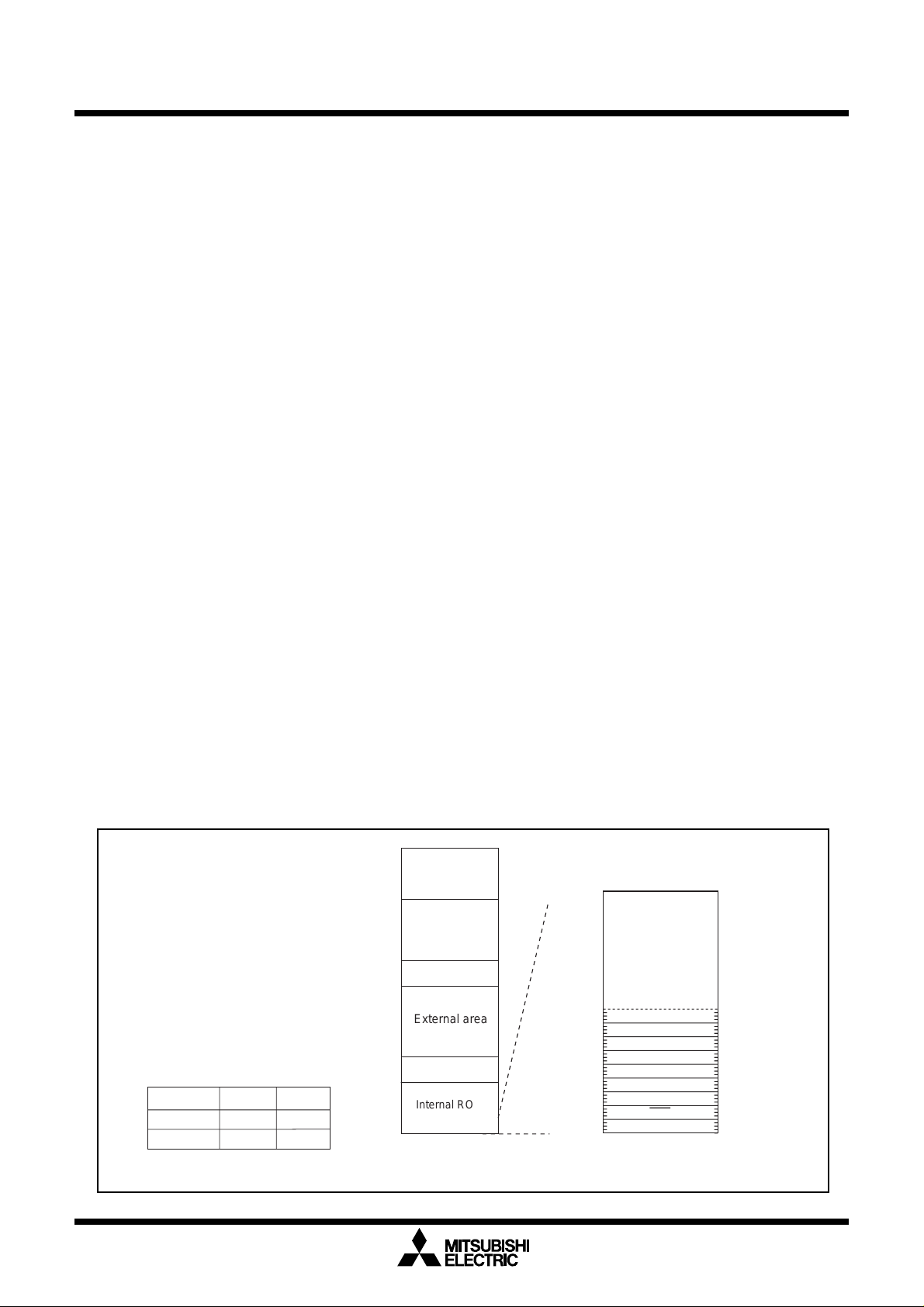
Memory
Figure 1.2.1 is a memory map of the M16C/80 group. The address space extends the 16 Mbytes from
address 00000016 to FFFFFF16. From FFFFFF16 down is ROM. For example, in the M30800MC-XXXFP,
there is 128K bytes of internal ROM from FE000016 to FFFFFF16. The vector table for fixed interrupts such
as the reset and NMI are mapped to FFFFDC16 to FFFFFF16. The starting address of the interrupt routine
is stored here. The address of the vector table for timer interrupts, etc., can be set as desired using the
internal register (INTB). See the section on interrupts for details.
From 00040016 up is RAM. For example, in the M30800MC-XXXFP, 10 Kbytes of internal RAM is mapped
to the space from 00040016 to 002BFF16. In addition to storing data, the RAM also stores the stack used
when calling subroutines and when interrupts are generated.
The SFR area is mapped to 00000016 to 0003FF16. This area accommodates the control registers for
peripheral devices such as I/O ports, A-D converter, serial I/O, and timers, etc. Figure 1.5.1 to 1.5.4 are
location of peripheral unit control registers. Any part of the SFR area that is not occupied is reserved and
cannot be used for other purposes.
The special page vector table is mapped to FFFE0016 to FFFFDB16. If the starting addresses of subroutines or the destination addresses of jumps are stored here, subroutine call instructions and jump instructions can be used as 2-byte instructions, reducing the number of program steps.
In memory expansion mode and microprocessor mode, a part of the spaces are reserved and cannot be
used. For example, in the M30800MC-XXXFP, the following spaces cannot be used.
• The space between 002C0016 and 00800016 (Memory expansion and microprocessor modes)
• The space between F0000016 and FDFFFF16 (Memory expansion mode)
_______
Type No.
M30800MC/FC
M30803MG/FG
Address
XXXXX
002BFF
0053FF
Figure 1.2.1. Memory map
10
000000
16
000400
XXXXXX
008000
16
F00000
16
Address
16
YYYYY
FE0000
16
16
FC0000
YYYYYY
16
16
FFFFFF
16
SFR area
For details, see
Figures 1.5.1 to
16
Internal RAM
16
Internal reserved
area (Note 1)
External area
AAAA
AAAA
Internal reserved
area (Note 2)
16
Internal ROM
16
1.5.4
area
area
FFFE00
FFFFDC
FFFFFF
16
Special page
vector table
16
Undefined instruction
Overflow
BRK instruction
Address match
Watchdog timer
16
Reset
NMI
Note 1: During memory expansion and microprocessor modes, can not be used.
Note 2: In memory expansion mode, can not be used.
Under
development
CPU
Preliminary Specifications REV.D
Specifications in this manual are tentative and subject to change.
M16C/80 (100-pin version) group
SINGLE-CHIP 16-BIT CMOS MICROCOMPUTER
Mitsubishi microcomputers
Central Processing Unit (CPU)
The CPU has a total of 28 registers shown in Figure 1.3.1. Seven of these registers (R0, R1, R2, R3, A0,
A1, SB and FB) come in two sets; therefore, these have two register banks.
General register
b31
R2
R3
b23
High-speed interrupt register
b23
b15 b0
FLG
R0H
R1H
A0
A1
SB
FB
USP
ISP
INTB
PC
b15 b0
SVP
R0L
R1L
R2
R3
SVF
Flag register
Data register (Note)
Address register (Note)
Static base register (Note)
Frame base register (Note)
User stack pointer
Interrupt stack pointer
Interrupt table register
Program counter
Flag save register
PC save register
VCT
DMAC related register
b15
b23
DMA0
DMA1
DSA0
DSA1
DRA0
DRA1
Note: These registers have two register banks.
Figure 1.3.1. Central processing unit register
b7 b0
DMD0
DMD1
DCT0
DCT1
DRC0
DRC1
Vector register
DMA mode register
DMA transfer count register
DMA transfer count reload register
DMA memory address register
DMA SFR address register
DMA memory address reload register
11

Under
development
CPU
Preliminary Specifications REV.D
Specifications in this manual are tentative and subject to change.
M16C/80 (100-pin version) group
SINGLE-CHIP 16-BIT CMOS MICROCOMPUTER
Mitsubishi microcomputers
(1) Data registers (R0, R0H, R0L, R1, R1H, R1L, R2, R3, R2R0 and R3R1)
Data registers (R0, R1, R2, and R3) are configured with 16 bits, and are used primarily for transfer and
arithmetic/logic operations.
Registers R0 and R1 each can be used as separate 8-bit data registers, high-order bits as (R0H/R1H),
and low-order bits as (R0L/R1L). Registers R2 and R0, as well as R3 and R1 can use as 32-bit data
registers (R2R0/R3R1).
(2) Address registers (A0 and A1)
Address registers (A0 and A1) are configured with 24 bits, and have functions equivalent to those of data
registers. These registers can also be used for address register indirect addressing and address register
relative addressing.
(3) Static base register (SB)
Static base register (SB) is configured with 24 bits, and is used for SB relative addressing.
(4) Frame base register (FB)
Frame base register (FB) is configured with 24 bits, and is used for FB relative addressing.
(5) Program counter (PC)
Program counter (PC) is configured with 24 bits, indicating the address of an instruction to be executed.
(6) Interrupt table register (INTB)
Interrupt table register (INTB) is configured with 24 bits, indicating the start address of an interrupt vector
table.
(7) User stack pointer (USP), interrupt stack pointer (ISP)
Stack pointer comes in two types: user stack pointer (USP) and interrupt stack pointer (ISP), each configured with 24 bits.
Your desired type of stack pointer (USP or ISP) can be selected by a stack pointer select flag (U flag).
This flag is located at the position of bit 7 in the flag register (FLG).
Set USP and ISP to an even number so that execution efficiency is increased.
(8) Save flag register (SVF)
This register consists of 16 bits and is used to save the flag register when a high-speed interrupt is
generated.
12

Under
development
CPU
Preliminary Specifications REV.D
Specifications in this manual are tentative and subject to change.
M16C/80 (100-pin version) group
SINGLE-CHIP 16-BIT CMOS MICROCOMPUTER
Mitsubishi microcomputers
(9) Save PC register (SVP)
This register consists of 24 bits and is used to save the program counter when a high-speed interrupt is
generated.
(10) Vector register (VCT)
This register consists of 24 bits and is used to indicate the jump address when a high-speed interrupt is
generated.
(11) DMA mode registers (DMD0/DMD1)
These registers consist of 8 bits and are used to set the transfer mode, etc. for DMA.
(12) DMA transfer count registers (DCT0/DCT1)
These registers consist of 16 bits and are used to set the number of DMA transfers performed.
(13) DMA transfer count reload registers (DRC0/DRC1)
These registers consist of 16 bits and are used to reload the DMA transfer count registers.
(14) DMA memory address registers (DMA0/DMA1)
These registers consist of 24 bits and are used to set a memory address at the source or destination of
DMA transfer.
(15) DMA SFR address registers (DSA0/DSA1)
These registers consist of 24 bits and are used to set a fixed address at the source or destination of DMA
transfer.
(16) DMA memory address reload registers (DRA0/DRA1)
These registers consist of 24 bits and are used to reload the DMA memory address registers.
13

Under
development
Preliminary Specifications REV.D
Specifications in this manual are tentative and subject to change.
CPU
(17) Flag register (FLG)
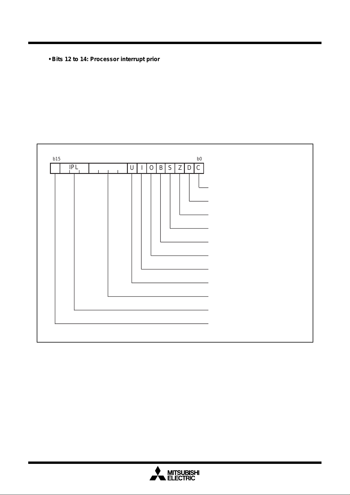
Flag register (FLG) is configured with 11 bits, each bit is used as a flag. Figure 1.3.2 shows the flag
register (FLG). The following explains the function of each flag:
• Bit 0: Carry flag (C flag)
This flag retains a carry, borrow, or shift-out bit that has occurred in the arithmetic/logic unit.
• Bit 1: Debug flag (D flag)
This flag enables a single-step interrupt.
When this flag is “1”, a single-step interrupt is generated after instruction execution. This flag is
cleared to “0” when the interrupt is acknowledged.
• Bit 2: Zero flag (Z flag)
This flag is set to “1” when an arithmetic operation resulted in 0; otherwise, cleared to “0”.
Mitsubishi microcomputers
M16C/80 (100-pin version) group
SINGLE-CHIP 16-BIT CMOS MICROCOMPUTER
• Bit 3: Sign flag (S flag)
This flag is set to “1” when an arithmetic operation resulted in a negative value; otherwise, cleared
to “0”.
• Bit 4: Register bank select flag (B flag)
This flag chooses a register bank. Register bank 0 is selected when this flag is “0” ; register bank
1 is selected when this flag is “1”.
• Bit 5: Overflow flag (O flag)
This flag is set to “1” when an arithmetic operation resulted in overflow; otherwise, cleared to “0”.
• Bit 6: Interrupt enable flag (I flag)
This flag enables a maskable interrupt.
An interrupt is disabled when this flag is “0”, and is enabled when this flag is “1”. This flag is
cleared to “0” when the interrupt is acknowledged.
• Bit 7: Stack pointer select flag (U flag)
Interrupt stack pointer (ISP) is selected when this flag is “0” ; user stack pointer (USP) is selected
when this flag is “1”.
This flag is cleared to “0” when a hardware interrupt is acknowledged or an INT instruction of
software interrupt Nos. 0 to 31 is executed.
14
• Bits 8 to 11: Reserved area
Under
development
CPU
Preliminary Specifications REV.D
Specifications in this manual are tentative and subject to change.
• Bits 12 to 14: Processor interrupt priority level (IPL)
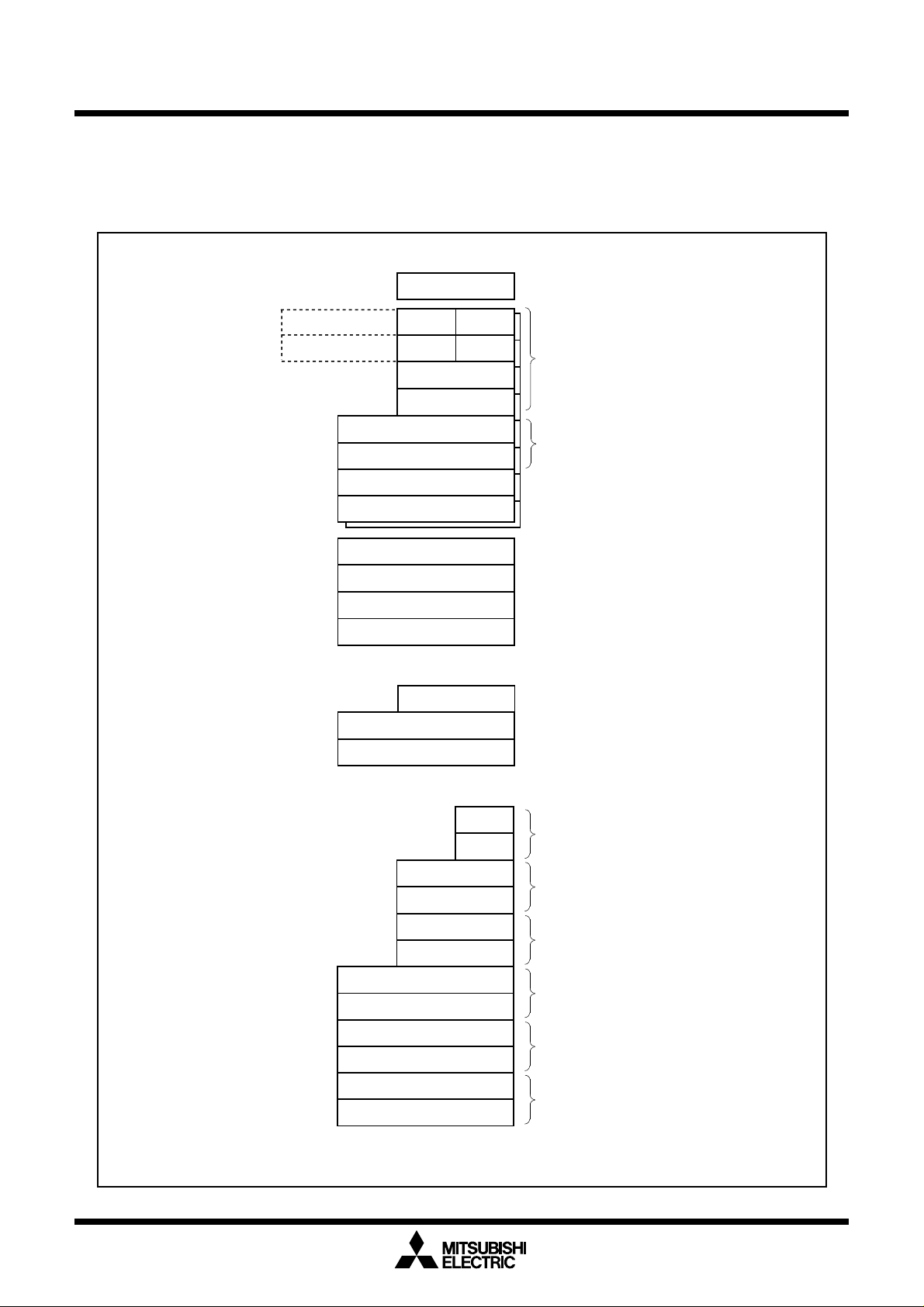
Processor interrupt priority level (IPL) is configured with three bits, for specification of up to eight
processor interrupt priority levels from level 0 to level 7.
If a requested interrupt has priority greater than the processor interrupt priority level (IPL), the interrupt
is enabled.
• Bit 15: Reserved area
b0b15
IPL
AAAAAAA
A
A
CDZSBOIU
M16C/80 (100-pin version) group
SINGLE-CHIP 16-BIT CMOS MICROCOMPUTER
Flag register (FLG)
Carry flag
Mitsubishi microcomputers
Figure 1.3.2. Flag register (FLG)
Debug flag
Zero flag
Sign flag
Register bank select flag
Overflow flag
Interrupt enable flag
Stack pointer select flag
Reserved area
Processor interrupt priority level
Reserved area
15
Under
development
Reset
Preliminary Specifications REV.D
Specifications in this manual are tentative and subject to change.
M16C/80 (100-pin version) group
SINGLE-CHIP 16-BIT CMOS MICROCOMPUTER
Mitsubishi microcomputers
Reset
There are two kinds of resets; hardware and software. In both cases, operation is the same after the reset.
(See “Software Reset” for details of software resets.) This section explains on hardware resets.
When the supply voltage is in the range where operation is guaranteed, a reset is effected by holding the
reset pin level “L” (0.2VCC max.) for at least 20 cycles. When the reset pin level is then returned to the “H”
level while main clock is stable, the reset status is cancelled and program execution resumes from the
address in the reset vector table.
Figure 1.4.1 shows the example reset circuit. Figure 1.4.2 shows the reset sequence.
RESET
Example when f(XIN) = 10MHz and V
V
Figure 1.4.1. Example reset circuit
X
IN
More than 20 cycles are needed
Microprocessor
mode BYTE = “H”
RESET
BCLK
Address
RD
BCLK 24cycles
CC
5V
V
CC
0V
5V
RESET
0V
FFFFC
CC
= 5V
16
4.2V
0.8V
.
Content of reset vector
FFFFD
16
FFFFE
16
WR
CS0
Microprocessor
mode BYTE = “L”
Address
RD
WR
CS0
Single chip
mode
Address
Figure 1.4.2. Reset sequence
16
FFFFC
FFFFC
16
16
FFFFE
FFFFE
16
Content of reset vector
16
Content of reset vector
Under
development
Reset
Preliminary Specifications REV.D
Specifications in this manual are tentative and subject to change.
Mitsubishi microcomputers
M16C/80 (100-pin version) group
SINGLE-CHIP 16-BIT CMOS MICROCOMPUTER
Table 1.4.1 shows the statuses of the other pins while the RESET pin level is “L”. Figures 1.4.3 and 1.4.4
____________
show the internal status of the microcomputer immediately after the reset is cancelled.
Table 1.4.1. Pin status when RESET pin level is “L”
____________
Status
Pin name
P0
P1
P2, P3, P4
P5
0
P5
1
P5
2
P5
3
P5
4
P5
5
P5
6
P5
7
P6, P7, P80 to P84,
P8
6
, P87, P9, P10
CNVSS = V
Input port (floating)
Input port (floating)
Input port (floating)
Input port (floating)
Input port (floating)
Input port (floating)
Input port (floating)
Input port (floating)
Input port (floating)
Input port (floating)
Input port (floating)
Input port (floating)
SS
CNVSS = V
BYTE = V
Data input (floating)
Data input (floating)
Address output (undefined)
WR output (“H” level is output)
BHE output (undefined)
RD output (“H” level is output)
BCLK output
HLDA output (The output value
depends on the input to the
HOLD pin)
HOLD input (floating)
RAS output
RDY input (floating)
Input port (floating) Input port (floating)
SS
CC
BYTE = V
Data input (floating)
Input port (floating)
Address output (undefined)
WR output (“H” level is output)
BHE output (undefined)
RD output (“H” level is output)
BCLK output
HLDA output (The output value
depends on the input to the
HOLD pin)
HOLD input (floating)
RAS output
RDY input (floating)
CC
17
Under
development
Reset
Preliminary Specifications REV.D
Specifications in this manual are tentative and subject to change.
16
(1) (0004
(2) (000516)···Processor mode register 1
(3) (0006
(4) (0007
(5) (0008
Address match interrupt
(6) (0009
enable register
(7) Protect register (000A
External data bus width control
(8)
(9)
(10)
(11)
register
register
(000B
(000C
(000F16)···Watchdog timer control
(0010
(0011
(0012
(12)
(0014
(0015
(001616)··· 00
(13)
Address match interrupt register 2
(0018
(001916)··· 00
(001A16)··· 00
(14)
Address match interrupt register 3
(001C16)··· 00
(001D16)··· 00
(001E16)··· 00
(15)
(16)
DMA0 interrupt control register
(17)
Timer B2 interrupt control register
(18)
DMA2 interrupt control register
UART2 receive/ACK interrupt control
(19)
register
(20)
Timer A0 interrupt control register
UART3 receive/ACK interrupt control
(21)
register
(22)
Timer A2 interrupt control register
UART4 receive/ACK interrupt control
(23)
register
(24)
Timer A4 interrupt control register
Bus collision detection(UART3)
(25)
interrupt control register
UART0 receive interrupt control
(26)
register
A-D conversion interrupt
(27)
control register
UART1 receive interrupt control
(28)
register
(29)
Timer B1 interrupt control register
The content of other registers and RAM is undefined when the microcomputer is reset. The initial values
must therefore be set.
Note: When the V
(004016)···DMAM control register ?????
(0068
(0069
(006A
(006B
(006C
(006D
(006E
(006F
(0070
(0071
(0072
(0073
(0074
(0076
CC
level is applied to the CNVSS pin, it is 0316 at a reset.
)···Processor mode register 0 (Note) 80
16
)···System clock control register 0
16
)···System clock control register 1
16
)···Wait control register
16
)···
16
)···
16
)···
16
)···Main clock divided register
16
)···Address match interrupt register 0
16
)···
16
)···
16
)···Address match interrupt register 1
16
)··· 00
16
)···
16
)···
16
)···
16
)···
16
)···
16
)···
16
)···
16
)···
16
)···
16
)···
16
)···
16
)···
16
)··· ? 0 0 0
16
)···
16
)···
x : Nothing is mapped to this bit
? : Undefined
16
00
16
08
16
20
16
FF
16
00
00
000
000
01
000
00?0????
00
16
00
16
00
16
00
16
16
16
00
16
16
16
16
16
16
?000
?000
?000
?000
?000
?000
?000
0 0 0?
? 0 0 0
? 0 0 0
? 0 0 0
? 0 0 0
? 0 0 0
M16C/80 (100-pin version) group
SINGLE-CHIP 16-BIT CMOS MICROCOMPUTER
(30)
Timer B3 interrupt control register
(31)
INT5 interrupt control register
(32)
INT3 interrupt control register
(33)
INT1 interrupt control register
(34)
DMA1 interrupt control register
UART2 transmit/NACK interrupt
(35)
control register
(36)
DMA3 interrupt control register
UART3 transmit/NACK interrupt
(37)
control register
(38)
Timer A1 interrupt control register
UART4 receive/NACK interrupt
(39)
control register
(40)
Timer A3 interrupt control register
Bus collision detection(UART2)
(41)
interrupt control register
UART0 transmit interrupt control register
(42)
Bus collision detection(UART4)
(43)
interrupt control register
(44)
UART1 transmit interrupt control register
(45)
Key input interrupt control register
(46)
Timer B0 interrupt control register
(47)
Timer B2 interrupt control register
Timer B4 interrupt control register
(48)
(49)
INT4 interrupt control register
(50)
INT2 interrupt control register
(51)
INT0 interrupt control register
(52)
Exit priority register
(53)
XY control register
(54)
UART4 special mode register 3
(55)
UART4 special mode register 2
(56)
UART4 special mode register
(57)
UART4 transmit/receive mode register
(58)
UART4 transmit/receive control register 0
(59)
UART4 transmit/receive control register 1
(60)
Timer B3,4,5 count start flag
(61)
Three-phase PWM control register 0
(62)
Three-phase PWM control register 1
(63)
Three-phase output buffer register 0
(64)
Three-phase output buffer register 1
(65)
Timer B3 mode register
(66)
Timer B4 mode register
(67)
Timer B5 mode register
Mitsubishi microcomputers
(007816)···
(007A
16
)···
00
(007C
16
)···
00
(007E
16
)···
00
(0088
16
)···
(0089
16
)···
(008A
16
)···
(008B
16
)···
(008C
16
)··· ? 0 0 0
(008D
16
)··· ? 0 0 0
(008E
16
)···
(008F
16
)···
(0090
16
)···
(0091
16
)···
(0092
16
)···
(009316)···
(0094
16
)···
(0096
16
)···
(0098
16
)··· ? 0 0 0
(009A
16
)··· ? 000
00
(009C
16
(009E
16
(009F
16
(02E0
16
16
(02F5
(02F6
16
(02F716)···
(02F816)···
(02FC16)···
(02FD16)···
(030016)···
(030816)··· 00
16
(0309
(030A
16
(030B16)···
(031B
16
(031C
16
(031D
16
00
)···
00
)···
)···
)···
00
)···
)···
16
00
00
00
08
02
000
)···
000 ?0000
)··· 00
00
)···
00? 0000
?
)···
00? 0000
)···
00? 0000
? 0 0 0
? 000
? 000
? 000
? 0 0 0
? 0 0 0
? 0 0 0
? 0 0 0
? 0 0 0
? 0 0 0
? 000
? 000
? 000
? 0 0 0
? 0 0 0
? 0 0 0
? 000
? 000
0 000
00
16
16
16
16
16
16
16
16
Figure 1.4.3. Device's internal status after a reset is cleared
18
Under
development
Reset
(68)
(69)
(70)
(71)
(72)
(73)
(74)
(75)
(76)
(77)
(78)
(79)
(80)
(81)
(82)
(83)
(84)
(85)
(86)
(87)
(88)
(89)
(90)
(91)
(92)
(93)
(94)
(95)
(96)
(97)
(98)
(99)
(100)
(101)
(102)
(103)
(104)
(105)
(106)
(107)
(108)
Preliminary Specifications REV.D
Specifications in this manual are tentative and subject to change.
Interrupt cause select register
UART3 special mode register 3
UART3 special mode register 2
UART3 special mode register
UART3 transmit/receive mode register
UART3 transmit/receive control register 0
UART3 transmit/receive control register 1
UART2 special mode register 3
UART2 special mode register 2
UART2 special mode register
UART2 transmit/receive mode register
UART2 transmit/receive control register 0
UART2 transmit/receive control register 1
Count start flag
Clock prescaler reset flag
One-shot start flag
Trigger select flag
Up-down flag
Timer A0 mode register
Timer A1 mode register
Timer A2 mode register
Timer A3 mode register
Timer A4 mode register
Timer B0 mode register
Timer B1 mode register
Timer B2 mode register
UART0 transmit/receive mode register
UART0 transmit/receive control register 0
UART0 transmit/receive control register 1
UART1 transmit/receive mode register
UART1 transmit/receive control register 0
UART1 transmit/receive control register 1
UART transmit/receive control register 2
(Note)
(Note)
DMA0 cause select register
DMA1 cause select register
DMA2 cause select register
DMA3 cause select register
A-D control register 2
A-D control register 0
(031F16)···
(0325
16
)···
(0326
16
)···
16
)···
(0327
16
)···
(0328
(032C16)···
(032D
16
)···
0 00
16
)···
(0335
16
)···
(0336
(0337
16
)··· 00
(033816)··· 00
(033C
16
)···
0010000
(033D
16
)···
16
)···
(0340
(0341
16
)···
0
16
)···
(0342
(034316)··· 00
(0344
16
)···
16
)···
(0356
(0357
(0358
(0359
(035A
(035B
(035C
(035D16)···
(0360
(0364
(0365
(0368
(036C
000 0?000
16
)···
000 0?000
16
)···
000 0?000
16
)···
000 0?000
16
)···
000 0?000
16
)··· 00? 0000?
16
)··· 00? 0000
00? 0000
16
)···
16
)···
16
)···
16
)···
16
)···
(036D16)···
(037016)··· 00 00000
?
?
16
)···Flash memory control register 0
(0377
(0378
16
000010
)··· 0
(037916)···
(037A
16
)··· 0
(037B16)···
(0394
16
)···
16
)···
(0396
000000
(109)
A-D control register 1
00
16
00
16
00
16
00
16
08
16
02
16
(110)
D-A control register
(111)
(112)
(113)
(114)
(115)
(116)
00
16
16
16
(117)
(118)
(119)
(120)
02
16
00
16
(121)
(122)
(123)
00
16
16
00
16
(124)
(125)
(126)
(127)
(128)
(129)
(130)
(131)
(132)
(133)
(132)
00
16
08
16
02
16
00
16
08
16
02
16
(135)
(136)
(137)
(138)
(139)
(140)
(141)
(142)
0?????(037616)···Flash memory control register 1
(143)
(144)
000000
(145)
0000000
(146)
000000
(147)
0000000
(148)
00000
???
(149)
00000
M16C/80 (100-pin version) group
SINGLE-CHIP 16-BIT CMOS MICROCOMPUTER
(0397
(039C
Function select register C
Function select register A0
Function select register A1
Function select register B0
Function select register B1
Function select register A2
Function select register A3
Function select register B2
Function select register B3
Port P6 direction register
Port P7 direction register
Port P8 direction register
Port P9 direction register
Port P10 direction register
Pull-up control register 2
Pull-up control register 3
Port P0 direction register
Port P1 direction register
Port P2 direction register
Port P3 direction register
Port P4 direction register
Port P5 direction register
Pull-up control register 0
Pull-up control register 1
Port control register
Data registers (R0/R1/R2/R3)
Address registers (A0/A1)
Static base register (SB)
Frame base register (FB)
Interrupt table register (INTB)
User stack pointer (USP)
Interrupt stack pointer (ISP)
Flag register (FLG)
DMA mode register (DMD0/DMD1)
DMA transfer count register (DCT0/DCT1)
DMA transfer count reload register
(DRC0/DRC1)
DMA memory address register (DMA0/DMA1)
DMA SFR address register (DSA0/DSA1)
DMA memory address reload register
(DRA0/DRA1)
(03AF
(03B0
(03B1
(03B2
(03B3
(03B4
(03B5
(03B6
(03B716)···
(03C2
(03C3
(03C6
(03C7
(03CA
(03DA
(03DB
(03E2
(03E3
(03E6
(03E7
(03EA
(03EB
(03F0
(03F116)··· X0
(03FF
Mitsubishi microcomputers
16
)··· 00
16
)··· 00
16
)···
16
)···
16
)···
16
)···
16
)···
16
)···
16
)···
16
)···
16
)···
16
)···
16
)···
16
)···
16
)···
16
)···
16
)···
16
)···
16
)···
16
)···
16
)···
16
)···
16
)···
16
)···
16
)···
0000
0
0
000000
000000
000000
000000
000000
000000
00
0
0
00
00
00
00
00
00
00
00
00
00
00
00
00
0000
0000
00
??
??
??
??
??
16
16
16
0
000000
00 0
0000000
?000??0?
16
16
0000000
16
16
16
16
16
16
16
16
16
16
16
16
16
16
16
16
16
16
16
16
16
0
00
0
0
x : Nothing is mapped to this bit
? : Undefined
The content of other registers and RAM is undefined when the microcomputer is reset. The initial values
must therefore be set.
Note :This register exists in the flash memory version.
Figure 1.4.4. Device's internal status after a reset is cleared
19

Under
development
SFR
Preliminary Specifications REV.D
Specifications in this manual are tentative and subject to change.
0060
0000
16
0001
16
0002
16
0003
16
0004
16
Processor mode register 0 (PM0)
0005
16
Processor mode register 1(PM1)
0006
16
System clock control register 0 (CM0)
0007
16
System clock control register 1 (CM1)
0008
16
Wait control register (WCR)
0009
16
Address match interrupt enable register (AIER)
000A
16
Protect register (PRCR)
000B
16
External data bus widthcontrol register (DS)
000C
16
Main clock division register (MCD)
000D
16
000E
16
Watchdog timer start register (WDTS)
000F
16
Watchdog timer control register (WDC)
0010
16
0011
16
Address match interrupt register 0 (RMAD0)
0012
16
0013
16
0014
16
0015
16
Address match interrupt register 1 (RMAD1)
0016
16
0017
16
0018
16
0019
16
Address match interrupt register 2 (RMAD2)
001A
16
001B
16
001C
16
Address match interrupt register 3 (RMAD3)
001D
16
001E
16
001F
16
0020
16
Emulator interrupt vector table register (EIAD)
0021
16
0022
16
0023
16
Emulator interrupt detect register (EITD)
0024
16
Emulator protect register (EPRR)
0025
16
0026
16
0027
16
0028
16
0029
16
002A
16
002B
16
002C
16
002D
16
002E
16
002F
16
0030
16
ROM areaset register (ROA)
0031
16
Debug monitor area set register (DBA)
0032
16
Expansion area set register 0 (EXA0)
0033
16
Expansion area set register 1 (EXA1)
0034
16
Expansion area set register 2 (EXA2)
0035
16
Expansion area set register 3 (EXA3)
0036
16
0037
16
0038
16
0039
16
003A
16
003B
16
003C
16
003D
16
003E
16
003F
16
0040
16
DRAM control register (DRAMCONT)
0041
16
DRAM reflesh interval set register (REFCNT)
0042
16
0043
16
0044
16
*
*
*
*
*
*
*
*
*
16
0061
16
0062
16
0063
16
0064
16
0065
16
0066
16
0067
16
0068
16
DMA0 interrupt control register (DM0IC)
0069
16
006A
16
DMA2 interrupt control register (DM1IC)
006B
16
006C
16
006D
16
006E
16
006F
16
0070
16
Timer A4 interrupt control register (TA4IC)
0071
16
Bus collision detection(UART3) interrupt control register (BCN3IC)
0072
16
UART0 receive interrupt control register (S0RIC)
0073
16
0074
16
0075
16
0076
16
Timer B1 interrupt control register (TB1IC)
0077
16
0078
16
0079
16
007A
16
007B
16
007C
16
007D
16
007E
16
007F
16
0080
16
0081
16
0082
16
0083
16
0084
16
0085
16
0086
16
0087
16
0088
16
0089
16
008A
16
008B
16
008C
16
008D
16
008E
16
Timer A3 interrupt control register (TA3IC)
008F
16
0090
16
0091
16
0092
16
0093
16
0094
16
0095
16
0096
16
Timer B2 interrupt control register (TB2IC)
0097
16
0098
16
0099
16
009A
16
009B
16
009C
16
INT2 interrupt control register (INT2IC)
009D
16
009E
16
009F
16
Exit priority register (RLVL)
00A0
16
00A1
16
00A2
16
00A3
16
00A4
16
Mitsubishi microcomputers
M16C/80 (100-pin version) group
SINGLE-CHIP 16-BIT CMOS MICROCOMPUTER
Timer B5 interrupt control register (TB5IC)
UART2 receive/ACK interrupt control register (S2RIC)
Timer A0 interrupt control register (TA0IC)
UART3 receive/ACK interrupt control register (S3RIC)
Timer A2 interrupt control register (TA2IC)
UART4 receive/ACK interrupt control register (S4RIC)
A-D conversion interrupt control register (ADIC)
UART1 receive interrupt control register (S1RIC)
Timer B3 interrupt control register (TB3IC)
INT5 interrupt control register (INT5IC)
INT3 interrupt control register (INT3IC)
INT1 interrupt control register (INT1IC)
DMA1 interrupt control register (DM1IC)
UART2 transmit/NACK interrupt control register (S2TIC)
DMA3 interrupt control register (DM3IC)
UART3 transmit/NACK interrupt control register (S3TIC)
Timer A1 interrupt control register (TA1IC)
UART4 transmit/NACK interrupt control register (S4TIC)
Bus collision detection(UART2) interrupt control register (BCN2IC)
UART0 transmit interrupt control register (S0TIC)
Bus collision detection(UART4) interrupt control register (BCN4IC)
UART1 transmit interrupt control register (S1TIC)
Key input interrupt control register (KUPIC)
Timer B0 interrupt control register (TB0IC)
Timer B4 interrupt control register (TB4IC)
INT4 interrupt control register (INT4IC)
INT0 interrupt control register (INT0IC)
As this register is used exclusively for debugger purposes, user cannot use this. Do not access to the register.
*
(The blank area is reserved and cannot be used by user.)
Figure 1.5.1. Location of peripheral unit control registers (1)
20

Under
development
SFR
02C0
02C1
02C2
02C3
02C4
02C5
02C6
02C7
02C8
02C9
02CA
02CB
02CC
02CD
02CE
02CF
02D0
02D1
02D2
02D3
02D4
02D5
02D6
02D7
02D8
02D9
02DA
02DB
02DC
02DD
02DE
02DF
02E0
02E1
02E2
02E3
02E4
02E5
02E6
02E7
02E8
02E9
02EA
02EB
02EC
02ED
02EE
02EF
02F0
02F1
02F2
02F3
02F4
02F5
02F6
02F7
02F8
02F9
02FA
02FB
02FC
02FD
02FE
02FF
Preliminary Specifications REV.D
Specifications in this manual are tentative and subject to change.
0300
16
X0 register (X0R) Y0 register (Y0R)
16
16
X1 register (X1R) Y1 register (Y1R)
16
16
X2 register (X2R) Y2 register (Y2R)
16
16
X3 register (X3R) Y3 register (Y3R)
16
16
X4 register (X4R) Y4 register (Y4R)
16
16
X5 register (X5R) Y5 register (Y5R)
16
16
X6 register (X6R) Y6 register (Y6R)
16
16
X7 register (X7R) Y7 register (Y7R)
16
16
X8 register (X8R) Y8 register (Y8R)
16
16
X9 register (X9R) Y9 register (Y9R)
16
16
X10 register (X10R) Y10 register (Y10R)
16
16
X11 register (X11R) Y11 register (Y11R)
16
16
X12 register (X12R) Y12 register (Y12R)
16
16
X13 register (X13R) Y13 register (Y13R)
16
16
X14 register (X14R) Y14 register (Y14R)
16
16
X15 register (X15R) Y15 register (Y15R)
16
16
XY control register (XYC)
16
16
16
16
16
16
16
16
16
16
16
16
16
16
16
16
16
16
16
16
16
UART4 special mode register 3 (U4SMR3) UART2 special mode register 3 (U2SMR3)
16
UART4 special mode register 2 (U4SMR2)
16
UART4 special mode register (U4SMR)
16
UART4 transmit/receive mode register (U4MR)
16
UART4 bit rate generator (U4BRG)
16
UART4 transmit buffer register (U4TB)
16
16
UART4 transmit/receive control register 0 (U4C0)
16
UART4 transmit/receive control register 1 (U4C1)
16
UART4 receive buffer register (U4RB)
16
(The blank area is reserved and cannot be used by user.)
16
Timer B3, 4, 5 count start flag (TBSR)
0301
16
0302
16
Timer A1-1 register (TA11)
0303
16
0304
16
Timer A2-1 register (TA21)
0305
16
0306
16
Timer A4-1 register (TA41)
0307
16
0308
16
Three-phase PWM control register 0(INVC0)
0309
16
Three-phase PWM control register 1(INVC1)
030A
16
Thrree-phase output buffer register 0(IDB0)
030B
16
Thrree-phase output buffer register 1(IDB1)
030C
16
Dead time timer(DTT)
Timer B2 interrupt occurrence frequency set counter(ICTB2)
030D
16
030E
16
030F
16
0310
16
Timer B3 register (TB3)
0311
16
0312
16
Timer B4 register (TB4)
0313
16
0314
16
Timer B5 register (TB5)
0315
16
0316
16
0317
16
0318
16
0319
16
031A
16
031B
16
Timer B3 mode register (TB3MR)
031C
16
Timer B4 mode register (TB4MR)
031D
16
Timer B5 mode register (TB5MR)
031E
16
031F
16
Interrupt cause select register (IFSR)
0320
16
0321
16
0322
16
0323
16
0324
16
0325
16
UART3 special mode register 3 (U3SMR3)
0326
16
UART3 special mode register 2 (U3SMR2)
0327
16
UART3 special mode register (U3SMR)
0328
16
UART3 transmit/receive mode register (U3MR)
UART3 bit rate generator (U3BRG)
0329
16
032A
16
UART3 transmit buffer register (U3TB)
032B
16
032C
16
UART3 transmit/receive control register 0 (U3C0)
032D
16
UART3 transmit/receive control register 1 (U3C1)
032E
16
UART3 receive buffer register (U3RB)
032F
16
0330
16
0331
16
0332
16
0333
16
0334
16
0335
16
0336
16
UART2 special mode register 2 (U2SMR2)
0337
16
UART2 special mode register (U2SMR)
0338
16
UART2 transmit/receive mode register (U2MR)
0339
16
UART2 bit rate generator (U2BRG)
033A
16
UART2 transmit buffer register (U2TB)
033B
16
033C
16
UART2 transmit/receive control register 0 (U2C0)
033D
16
UART2 transmit/receive control register 1 (U2C1)
033E
16
UART2 receive buffer register (U2RB)
033F
16
M16C/80 (100-pin version) group
SINGLE-CHIP 16-BIT CMOS MICROCOMPUTER
Mitsubishi microcomputers
Figure 1.5.2. Location of peripheral unit control registers (2)
21
Under
development
SFR
Preliminary Specifications REV.D
Specifications in this manual are tentative and subject to change.
0340
16
Count start flag (TABSR)
0341
16
Clock prescaler reset flag (CPSRF)
0342
16
One-shot start flag (ONSF)
0343
16
Trigger select register (TRGSR)
0344
16
Up-down flag (UDF)
0345
16
0346
16
Timer A0 register (TA0)
0347
16
0348
16
Timer A1 register (TA1)
0349
16
034A
16
Timer A2 register (TA2)
034B
16
034C
16
Timer A3 register (TA3)
034D
16
034E
16
Timer A4 register (TA4)
034F
16
0350
16
Timer B0 register (TB0)
0351
16
0352
16
Timer B1 register (TB1)
0353
16
0354
16
Timer B2 register (TB2)
0355
16
0356
16
Timer A0 mode register (TA0MR)
0357
16
Timer A1 mode register (TA1MR)
0358
16
Timer A2 mode register (TA2MR)
0359
16
Timer A3 mode register (TA3MR)
035A
16
Timer A4 mode register (TA4MR)
035B
16
Timer B0 mode register (TB0MR)
035C
16
Timer B1 mode register (TB1MR)
035D
16
Timer B2 mode register (TB2MR)
035E
16
035F
16
0360
16
UART0 transmit/receive mode register (U0MR)
0361
16
UART0 bit rate generator (U0BRG)
0362
16
UART0 transmit buffer register (U0TB)
0363
16
0364
16
UART0 transmit/receive control register 0 (U0C0)
0365
16
UART0 transmit/receive control register 1 (U0C1)
0366
16
UART0 receive buffer register (U0RB)
0367
16
0368
16
UART1 transmit/receive mode register (U1MR)
0369
16
UART1 bit rate generator (U1BRG)
036A
16
UART1 transmit buffer register (U1TB)
036B
16
036C
16
UART1 transmit/receive control register 0 (U1C0)
036D
16
UART1 transmit/receive control register 1 (U1C1)
036E
16
UART1 receive buffer register (U1RB)
036F
16
0370
16
UART transmit/receive control register 2 (UCON2)
0371
16
0372
16
0373
16
0374
16
0375
16
0376
16
Flash memory control register 1 (FMR1) (Note)
0377
16
Flash memory control register 0 (FMR0) (Note)
0378
16
DMA0 request cause select register (DM0SL)
0379
16
DMA1 request cause select register (DM1SL)
037A
16
DMA2 request cause select register (DM2SL)
037B
16
DMA3 request cause select register (DM3SL)
037C
16
CRC data register (CRCD)
037D
16
037E
16
CRC input register (CRCIN)
037F
16
Note :This register exists in the flash memory version.
Mitsubishi microcomputers
M16C/80 (100-pin version) group
SINGLE-CHIP 16-BIT CMOS MICROCOMPUTER
0380
16
A-D register 0 (AD0)
0381
16
0382
16
A-D register 1 (AD1)
0383
16
0384
16
A-D register 2 (AD2)
0385
16
0386
16
A-D register 3 (AD3)
0387
16
0388
16
A-D register 4 (AD4)
0389
16
038A
16
A-D register 5 (AD5)
038B
16
038C
16
A-D register 6 (AD6)
038D
16
038E
16
A-D register 7 (AD7)
038F
16
0390
16
0391
16
0392
16
0393
16
0394
16
A-D control register 2 (ADCON2)
0395
16
0396
16
A-D control register 0 (ADCON0)
0397
16
A-D control register 1 (ADCON1)
0398
16
D-A register 0 (DA0)
0399
16
039A
16
D-A register 1 (DA1)
039B
16
039C
16
D-A control register (DACON)
039D
16
039E
16
039F
16
03A0
16
03A1
16
03A2
16
03A3
16
03A4
16
03A5
16
03A6
16
03A7
16
03A8
16
03A9
16
03AA
16
03AB
16
03AC
16
03AD
16
03AE
16
03AF
16
Function select register C(PSC)
03B0
16
Function select register A0 (PS0)
03B1
16
Function select register A1 (PS1)
03B2
16
Function select register B0 (PSL0)
03B3
16
Function select register B1 (PSL1)
03B4
16
Function select register A2 (PS2)
03B5
16
Function select register A3 (PS3)
03B6
16
Function select register B2 (PSL2)
03B7
16
Function select register B3 (PSL3)
03B8
16
03B9
16
03BA
16
03BB
16
03BC
16
03BD
16
03BE
16
03BF
16
(The blank area is reserved and cannot be used by user.)
Figure 1.5.3. Location of peripheral unit control registers (3)
22
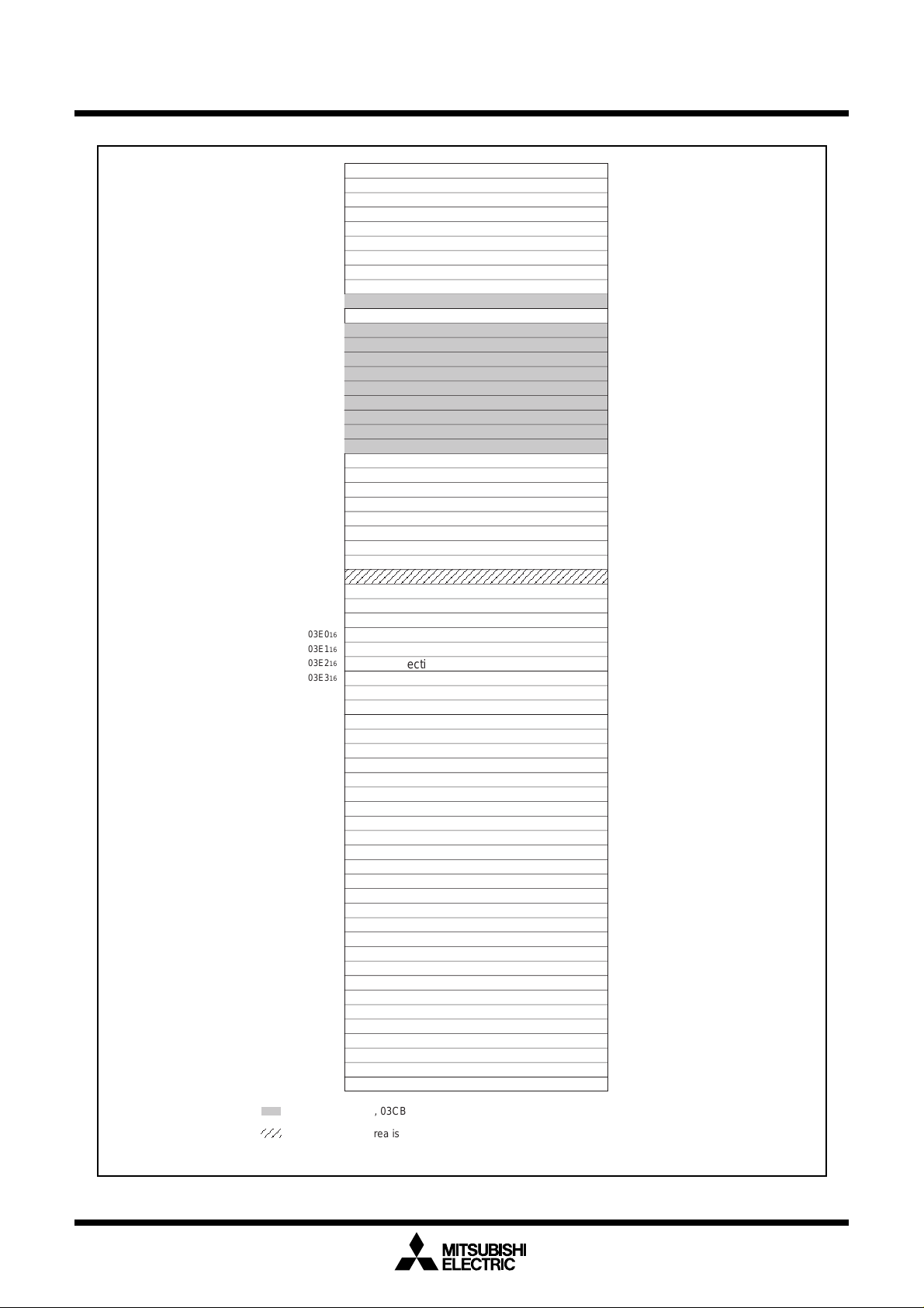
Under
AAAAAAAAAAAA
development
SFR
Preliminary Specifications REV.D
Specifications in this manual are tentative and subject to change.
03C016
Port P6 (P6)
03C116
Port P7 (P7)
03C216
Port P6 direction register (PD6)
03C316
Port P7 direction register (PD7)
03C416
Port P8 (P8)
03C516
Port P9 (P9)
03C616
Port P8 direction register (PD8)
03C716
Port P9 direction register (PD9)
03C816
Port P10 (P10)
03C916
03CA16
Port P10 direction register (PD10)
03CB16
03CC16
03CD16
03CE16
03CF16
03D016
03D116
03D216
03D316
03D416
03D516
03D616
03D716
03D816
03D916
03DA16
Pull-up control register 2 (PUR2)
03DB16
Pull-up control register 3 (PUR3)
03DC16
03DD16
03DE16
03DF16
03E016
Port P0 (P0)
03E116
Port P1 (P1)
03E216
Port P0 direction register (PD0)
03E316
Port P1 direction register (PD1)
03E416
Port P2 (P2)
03E516
Port P3 (P3)
03E616
Port P2 direction register (PD2)
03E716
Port P3 direction register (PD3)
03E816
Port P4 (P4)
03E916
Port P5 (P5)
03EA16
Port P4 direction register (PD4)
03EB16
Port P5 direction register (PD5)
03EC16
03ED16
03EE16
03EF16
03F016
Pull-up control register 0 (PUR0)
03F116
Pull-up control register 1 (PUR1)
03F216
03F316
03F416
03F516
03F616
03F716
03F816
03F916
03FA16
03FB16
03FC16
03FD16
03FE16
03FF16
Port control register (PCR)
Note 1: Addresses 03C916, 03CB16 to 03D316 area is for future plan.
Must set "FF
Note 2: Address 03DC
(The blank area is reserved and cannot be used by user.)
16" to address 03CB16, 03CE16, 03CF16, 03D216, 03D316 at initial setting.
16 area is for future plan. Must set "0016" to address 03DC16 at initial setting.
Mitsubishi microcomputers
M16C/80 (100-pin version) group
SINGLE-CHIP 16-BIT CMOS MICROCOMPUTER
Figure 1.5.4. Location of peripheral unit control registers (4)
23

Under
development
Preliminary Specifications REV.D
Specifications in this manual are tentative and subject to change.
Software Reset
M16C/80 (100-pin version) group
SINGLE-CHIP 16-BIT CMOS MICROCOMPUTER
Mitsubishi microcomputers
Software Reset
Writing “1” to bit 3 of the processor mode register 0 (address 000416) applies a (software) reset to the
microcomputer. A software reset has the same effect as a hardware reset. The contents of internal RAM
are preserved.
Processor Mode
(1) Types of Processor Mode
One of three processor modes can be selected: single-chip mode, memory expansion mode, and microprocessor mode. The functions of some pins, the memory map, and the access space differ according to
the selected processor mode.
• Single-chip mode
In single-chip mode, only internal memory space (SFR, internal RAM, and internal ROM) can be
accessed. Ports P0 to P10 can be used as programmable I/O ports or as I/O ports for the internal
peripheral functions.
• Memory expansion mode
In memory expansion mode, external memory can be accessed in addition to the internal memory
space (SFR, internal RAM, and internal ROM).
In this mode, some of the pins function as the address bus, the data bus, and as control signals. The
number of pins assigned to these functions depends on the bus and register settings. (See “Bus
Settings” for details.)
• Microprocessor mode
In microprocessor mode, the SFR, internal RAM, and external memory space can be accessed. The
internal ROM area cannot be accessed.
In this mode, some of the pins function as the address bus, the data bus, and as control signals. The
number of pins assigned to these functions depends on the bus and register settings. (See “Bus
Settings” for details.)
(2) Setting Processor Modes
24
The processor mode is set using the CNVSS pin and the processor mode bits (bits 1 and 0 at address
000416). Do not set the processor mode bits to “102”.
Regardless of the level of the CNVSS pin, changing the processor mode bits selects the mode. Therefore,
never change the processor mode bits when changing the contents of other bits. Also do not attempt to
shift to or from the microprocessor mode within the program stored in the internal ROM area.
• Applying VSS to CNVSS pin
The microcomputer begins operation in single-chip mode after being reset. Memory expansion mode
is selected by writing “012” to the processor mode is selected bits.
• Applying VCC to CNVSS pin
The microcomputer starts to operate in microprocessor mode after being reset.
Figure 1.6.1 and 1.6.2 show the processor mode register 0 and 1.
Figure 1.6.3 shows the memory maps applicable for each processor modes.
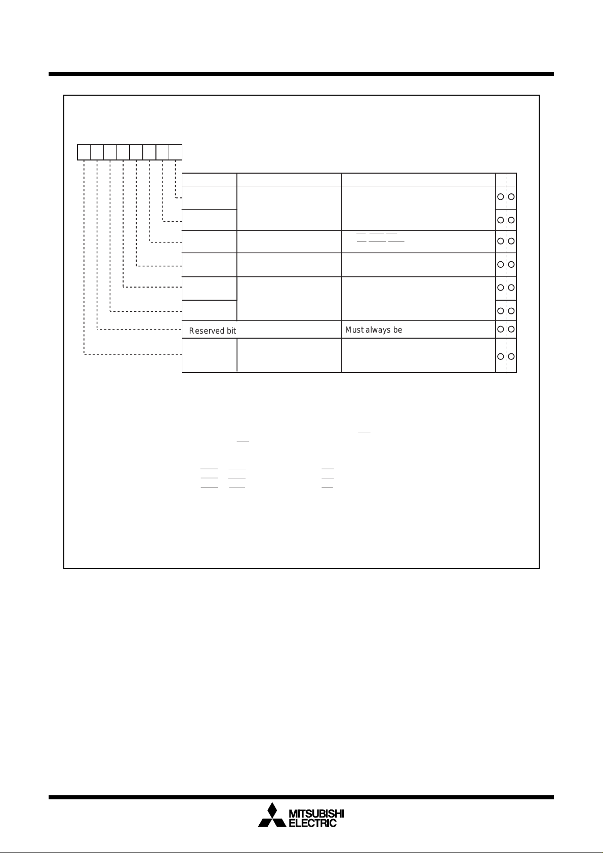
Under
development
Processor Mode
Specifications in this manual are tentative and subject to change.
Processor mode register 0 (Note 1)
b7 b6 b5 b4 b3 b2 b1 b0
0
Preliminary Specifications REV.D
Symbol Address When reset
PM0 0004
16
80
16
(Note 2)
Mitsubishi microcomputers
M16C/80 (100-pin version) group
SINGLE-CHIP 16-BIT CMOS MICROCOMPUTER
Bit name FunctionBit symbol
PM00
PM01
PM02
Processor mode bit
R/W mode select bit
(Note 7)
PM03
PM04
Software reset bit
Multiplexed bus space
select bit (Note 3)
PM05
Reserved bit
PM07
BCLK output disable bit
(Note 5)
Note 1: Set bit 1 of the protect register (address 000A
Note 2: If the V
CC
voltage is applied to the CNVSS, the value of this register when reset is 0316. (PM00 is set
16
b1 b0
0 0: Single-chip mode
0 1: Memory expansion mode
1 0: Inhibited
1 1: Microprocessor mode
0 : RD,BHE,WR
1 : RD,WRH,WRL
The device is reset when this bit is set to “1”.
The value of this bit is “0” when read.
b5 b4
0 0 : Multiplexed bus is not used
0 1 : Allocated to CS2 space
1 0 : Allocated to CS1 space
1 1 : Allocated to entire space (Note4)
Must always be set to “0”
0 : BCLK is output (Note 6)
1 : Function set by bit 0,1 of system
clock control register 0
) to “1” when writing new values to this register.
to “1” and PM07 is set to “0”.)
Note 3: Valid in microprocessor and memory expansion modes 1, 2 and 3. Do not use multiplex bus when
mode 0 is selected. Do not set to allocated to CS2 space when mode 2 is selected.
Note 4: After the reset has been released, the M16C/80 group MCU operates using the separate bus. As a
result, in microprocessor mode, you cannot select the full CS space multiplex bus.
When you select the full CS space multiplex bus in memory expansion mode, the address bus
operates with 64 Kbytes boundaries for each chip select.
Mode 0: Multiplexed bus cannot be used.
Mode 1: CS0 to CS2 when you select full CS space.
Mode 2: CS0 to CS1 when you select full CS space.
Mode 3: CS0 to CS3 when you select full CS space.
Note 5: No BCLK is output in single chip mode even when "0" is set in PM07. When stopping clock output in
microprocessor or memory expansion mode, make the following settings: PM07="1", bit 0 (CM00) and
16
bit 1 (CM01) of system clock control register 0 (address 0006
) = "0". "L" is now output from P53.
Note 6: When selecting BCLK, set bits 0 and 1 of system clock control register 0 (CM00, CM01) to "0".
Note 7: When using 16-bit bus width in DRAM controler, set this bit to "1".
WR
Figure 1.6.1. Processor mode register 0
25
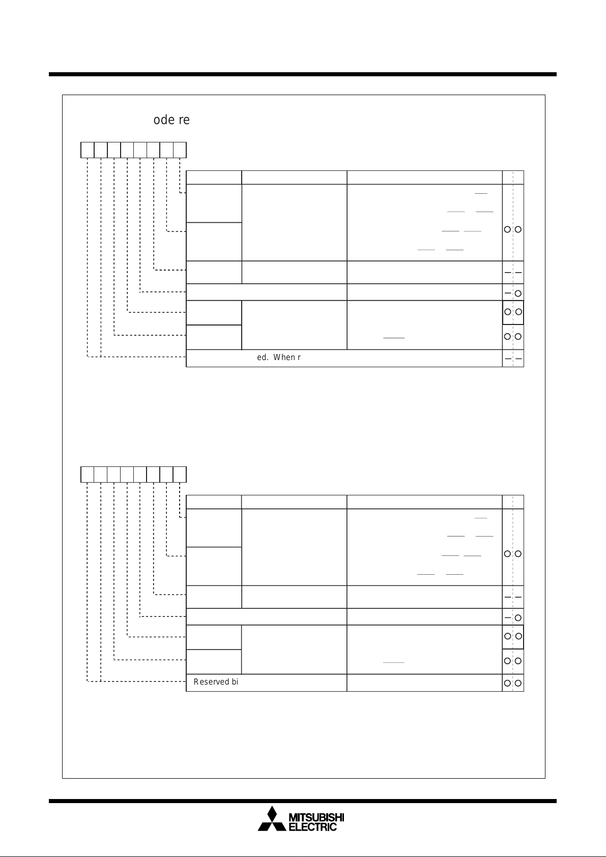
Under
development
Processor Mode
Specifications in this manual are tentative and subject to change.
Processor mode register 1 (Note 1) :Mask ROM version
b7 b6 b5 b4 b3 b2 b1 b0
Preliminary Specifications REV.D
Mitsubishi microcomputers
M16C/80 (100-pin version) group
SINGLE-CHIP 16-BIT CMOS MICROCOMPUTER
Symbol Address When reset
0
PM1 0005
16
00
16
Bit name FunctionBit symbol
PM10
External memory area
mode bit (Note 3)
b1 b0
0 0 : Mode 0 (P4
0 1 : Mode 1 (P4
P4
PM11
1 0 : Mode 2 (P4
P4
1 1 : Mode 3 (Note 2)
4
to P47 : CS3 to CS0)
(P4
PM12
Internal memory wait bit 0 : No wait state
1 : Wait state inserted
Reserved bit
PM14
PM15
ALE pin select bit (Note 3)
Must always be set to “0”
b5 b4
0 0 : No ALE
3
0 1 : P5
1 0 : P5
1 1 : P5
/BCLK (Note 4)
6
/RAS
4
/HLDA
Nothing is assinged. When read, the content is indeterminate.
Note 1: Set bit 1 of the protect register (address 000A16) to “1” when writing new values to this register.
Note 2: When mode 3 is selected, DRAMC is not used.
Note 3: Valid in memory expansion mode or in microprocessor mode.
3
Note 4: When selecting P5
/BCLK, set bits 0 and 1 of system clock control register 0 (CM00, CM01) to "0".
Processor mode register 1 (Note 1) :Flash memory version
b7 b6 b5 b4 b3 b2 b1 b0
0
Symbol Address When reset
PM1 0005
16
00
16
4
to P47 : A20 to A23)
4
: A20,
5
to P47 : CS2 to CS0)
4
, P45 : A20, A21,
6
, P47 : CS1, CS0)
WR
PM10
External memory area
mode bit (Note 3)
PM11
PM12
Internal memory wait bit 0 : No wait state
Reserved bit
PM14
PM15
ALE pin select bit (Note 3)
Reserved bit
Note 1: Set bit 1 of the protect register (address 000A16) to “1” when writing new values to this register.
Note 2: When mode 3 is selected, DRAMC is not used.
Note 3: Valid in memory expansion mode or in microprocessor mode.
3
Note 4: When selecting P5
/BCLK, set bits 0 and 1 of system clock control register 0 (CM00, CM01) to "0".
Figure 1.6.2. Processor mode register 1
Bit name FunctionBit symbol
b1 b0
4
0 0 : Mode 0 (P4
0 1 : Mode 1 (P4
P4
1 0 : Mode 2 (P4
P4
to P47 : A20 to A23)
4
: A20,
5
to P47 : CS2 to CS0)
4
, P45 : A20, A21,
6
, P47 : CS1, CS0)
WR
1 1 : Mode 3 (Note 2)
4
to P47 : CS3 to CS0)
(P4
1 : Wait state inserted
Must always be set to “0”
b5 b4
0 0 : No ALE
3
0 1 : P5
1 0 : P5
1 1 : P5
/BCLK (Note 4)
6
/RAS
4
/HLDA
Must always be set to “1”
26
Under
Singl chip
mode
Memory expanded mode
Microprocesser mode
SFR area
Internal RAM area
Internal reserved area
Internal ROM area
No use
External area
CS2
2Mbytes
CS0
2Mbytes
No use
Internal ROM area
Internal reserved area
Internal ROM area
Internal reserved area
Internal ROM area
Internal reserved area
CS0
3Mbytes
CS1
4Mbytes
(Note2)
CS1
2Mbytes
(Note1)
External area
CS2
2Mbytes
No use
CS0
2Mbytes
CS0
4Mbytes
CS1
4Mbytes
(Note2)
000000
16
000400
16
000800
16
200000
16
400000
16
C00000
16
E00000
16
F00000
16
FFFFFF
16
Each CS0, CS1 and CS can set 0 to 3 WAIT.
Mode 0
Mode 1 Mode 2 Mode 0
MOde 1 Mode 2
SFR area
Internal RAM area
Internal reserved area
SFR area
Internal RAM area
Internal reserved area
SFR area
Internal RAM area
Internal reserved area
SFR area
Internal RAM area
Internal reserved area
SFR area
Internal RAM area
Internal reserved area
SFR area
Internal RAM area
Mode 3
Internal reserved area
SFR area
Internal RAM area
Internal ROM area
Internal reserved area
CS1
1Mbytes
Mode 3
Internal reserved area
SFR area
Internal RAM area
No use
CS2
1Mbytes
No use
Connect with
DRAM
0.05 to 8MB
(When not
connect with
DRAM, use as
external area.)
External area
Connect with
DRAM
0.05 to 8MB
(When open area
is under 8MB,
cannot use the
rest of this area.)
Connect with
DRAM
0.05 to 8MB
(When open area
is under 8MB,
cannot use the
rest of this area.)
Connect with
DRAM
0.05 to 8MB
(When open area
is under 8MB,
cannot use the
rest of this area.)
No use
(Cannot use as
DRAM area or
external area.)
Connect with
DRAM
0.05 to 8MB
(When not
connect with
DRAM, use as
external area.)
Connect with
DRAM
0.05 to 8MB
(When open area
is under 8MB,
cannot use the
rest of this area.)
No use
(Cannot use as
DRAM area or
external area.)
External area
No use
CS3
1Mbytes
CS0
1Mbytes
CS1
1Mbytes
No use
CS2
1Mbytes
No use
CS1
2Mbytes
(Note1)
No use
CS3
1Mbytes
CS0
1Mbytes
development
Processor Mode
Processor Mode
Preliminary Specifications REV.D
Specifications in this manual are tentative and subject to change.
Mitsubishi microcomputers
M16C/80 (100-pin version) group
SINGLE-CHIP 16-BIT CMOS MICROCOMPUTER
Figure 1.6.3. Memory maps in each processor mode (without memory area expansion, normal mode)
27
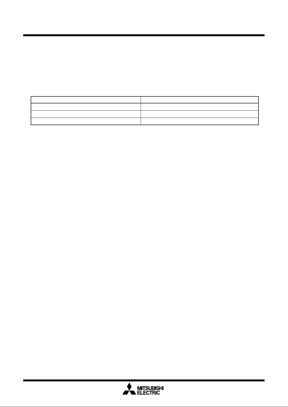
Under
development
Bus Settings
Preliminary Specifications REV.D
Specifications in this manual are tentative and subject to change.
M16C/80 (100-pin version) group
SINGLE-CHIP 16-BIT CMOS MICROCOMPUTER
Mitsubishi microcomputers
Bus Settings
The BYTE pin, bit 0 to 3 of the external data bus width control register (address 000B16), bits 4 and 5 of the
processor mode register 0 (address 000416) and bit 0 and 1 of the processor mode register 1 (address
000516) are used to change the bus settings.
Table 1.7.1 shows the factors used to change the bus settings, figure 1.7.1 shows external data bus width
control register and table 1.7.2 shows external area 0 to 3 and external area mode.
Table 1.7.1. Factors for switching bus settings
Bus setting Switching factor
Switching external address bus width External data bus width control register
Switching external data bus width BYTE pin (external area 3 only)
Switching between separate and multiplex bus Bits 4 and 5 of processor mode register 0
(1) Selecting external address bus width
You can select the width of the address bus output externally from the 16 Mbytes address space, the
number of chip select signals, and the address area of the chip select signals. (Note, however, that when
you select “Full CS space multiplex bus”, addresses A0 to A15 are output.) The combination of bits 0 and
1 of the processor mode register 1 allow you to set the external area mode.
When using DRAM controller, the DRAM area is output by multiplexing of the time splitting of the row and
column addresses.
____
(2) Selecting external data bus width
You can select 8-bit or 16-bit for the width of the external data bus for external areas 0, 1, 2, and 3. When
the data bus width bit of the external data bus width control register is “0”, the data bus width is 8 bits;
when “1”, it is 16 bits. The width can be set for each of the external areas. The default bus width for
external area 3 is 16 bits when the BYTE pin is “L” after a reset, or 8 bits when the BYTE pin is “H” after
a reset. The bus width selection is valid only for the external bus (the internal bus width is always 16 bits).
During operation, fix the level of the BYTE pin to “H” or “L”.
(3) Selecting separate/multiplex bus
The bus format can be set to multiplex or separate bus using bits 4 and 5 of the processor mode register 0.
• Separate bus
In this bus configuration, input and output is performed on separate data and address buses. The data
bus width can be set to 8 bits or 16 bits using the external data bus width control register. For all
programmable external areas, P0 is the data bus when the external data bus is set to 8 bits, and P1 is
a programmable IO port. When the external data bus width is set to 16 bits for any of the external
areas, P0 and P1 (although P1 is undefined for any 8-bit bus areas) are the data bus.
When accessing memory using the separate bus configuration, you can select a software wait using
the wait control register.
• Multiplex bus
In this bus configuration, data and addresses are input and output on a time-sharing basis. For areas
for which 8-bit has been selected using the external data bus width control register, the 8 bits D0 to D7
are multiplexed with the 8 bits A0 to A7. For areas for which 16-bit has been selected using the
external data bus width control register, the 16 bits D0 to D15 are multiplexed with the 16 bits A0 to
A15. When accessing memory using the multiplex bus configuration, two waits are inserted regardless of whether you select “No wait” or “1 wait’ in the appropriate bit of the wait control register.
28
Under
development
Specifications in this manual are tentative and subject to change.
Bus Settings
Preliminary Specifications REV.D
Mitsubishi microcomputers
M16C/80 (100-pin version) group
SINGLE-CHIP 16-BIT CMOS MICROCOMPUTER
The default after a reset is the separate bus configuration, and the full CS space multiplex bus configu-
____
____
ration cannot be selected in microprocessor mode. If you select “Full CS space multiplex bus”, the 16
bits from A0 to A15 are output for the address
External data bus width control register
b7 b6 b5 b4 b3 b2 b1 b0
Symbol Address When reset
DS 000B
16
XXXXX000
2
Bit name FunctionBit symbol
DS0
DS1
DS2
DS3
Nothing is assigned.
When write, set "0". When read, their contents are indeterminate.
Note: The value after a reset is determined by the input via the BYTE pin.
External area 0 data bus
width bit
External area 1 data bus
width bit
External area 2 data bus
width bit
External area 3 data bus
width bit (Note)
0 : 8 bits data bus width
1 : 16 bits data bus width
0 : 8 bits data bus width
1 : 16 bits data bus width
0 : 8 bits data bus width
1 : 16 bits data bus width
0 : 8 bits data bus width
1 : 16 bits data bus width
WR
Figure 1.7.1. External data bus width control register
Table 1.7.2. External area 0 to 3 and external area mode
External area mode
Memory expansion mode
Microprocessor mode
area 0
External
Memory expansion mode
Microprocessor mode
area 1
External
Memory expansion mode
Microprocessor mode
area 2
External
Memory expansion mode
area 3
External
Microprocessor mode
(Note 2)
,
,
,
Mode 0 Mode 1 Mode 2 Mode 3
00800016 to
1FFFFF
16
20000016 to
3FFFFF
16
40000016 to
BFFFFF
16
(Note 1)
C0000016 to
EFFFFF
16
C0000016 to
FFFFFF
16
<CS1 area>
16
008000
1FFFFF
to
16
<CS2 area>
16
200000
3FFFFF
to
16
<DRAMC area>
16
400000
BFFFFF
to
16
<CS0 area>
16
C00000
EFFFFF
to
16
<CS0 area>
16
E00000
FFFFFF
to
16
<CS1 area>
16
008000
1FFFFF
to
16
No area is
selected.
<DRAMC area>
16
400000
BFFFFF
to
16
<CS0 area>
16
C00000
EFFFFF
to
16
<CS0 area>
16
C00000
FFFFFF
to
16
<CS1 area>
100000
1FFFFF
<CS2 area>
200000
2FFFFF
<CS3 area>
C00000
CFFFFF
<CS0 area>
E00000
EFFFFF
<CS0 area>
F00000
FFFFFF
16
16
16
16
16
to
16
to
16
to
16
to
16
to
16
Note 1: DRAMC area when using DRAMC.
Note 2:Set the external area mode (modes 0, 1, 2, and 3) using bits 0 and 1 of the processor mode register
1 (address 000516).
29
Under
development
Bus Settings
Specifications in this manual are tentative and subject to change.
Table 1.7.3. Each processor mode and port function
Preliminary Specifications REV.D
Processor
mode
Single-chip
mode
Memory expansion mode/microprocessor modes
Mitsubishi microcomputers
M16C/80 (100-pin version) group
SINGLE-CHIP 16-BIT CMOS MICROCOMPUTER
Memory
expansion mode
Multiplexed
bus space
select bit
Data bus width
BYTE pin level
“01”, “10”
CS1 or CS2 : multiplexed
bus, and the other :
separate bus
All external
area is 8 bits
Some external
area is 16 bits
Separate bus
All external
area is 8 bits
“00”
Some external
area is 16 bits
“11” (Note 1)
All space multiplexed
bus
P00 to P07I/O port Data bus Data bus Data bus Data bus I/O port I/O port
P10 to P1
7
I/O port I/O port Data bus I/O port Data bus I/O port I/O
port
0
to P2
7
P2
P30 to P3
0
to P4
P4
4
to P4
P4
I/O port
7
I/O port
3
I/O port Address bus Address bus Address bus Address bus I/O port I/O port
6
I/O port CS (chip select) or address bus (A23)
Address bus Address bus
/data bus /data bus
(Note 2)
Address bus Address bus
(Note 2)
/data bus
(Note 2)
Address bus Address bus Address bus Address bus
/data bus /data bus
Address bus Address bus Address bus Address bus
/data bus
(For details, refer to “Bus control”) (Note 5)
P4
7
I/O port
CS (chip select) or address bus (A23)
(For details, refer to “Bus control”) (Note 5)
P5
0
to P5
3
I/O port
Outputs RD, WRL, WRH, and BCLK or RD, BHE, WR, and BCLK
(For details, refer to “Bus control”) (Note 3,4)
P5
P5
P5
P5
4
5
6
7
I/O port HLDA(Note 3) HLDA(Note 3) HLDA(Note 3) HLDA(Note 3) HLDA(Note 3) HLDA(Note 3)
I/O port HOLD HOLD HOLD HOLD HOLD HOLD
I/O port RAS (Note 3) RAS (Note 3) RAS (Note 3) RAS (Note 3) RAS (Note 3) RAS (Note 3)
I/O port RDY RDY RDY RDY RDY RDY
Note 1:The default after a reset is the separate bus configuration, and "Full CS space multiplex bus" cannot be selected in
microprocessor mode. When you select "Full CS space multiplex bus" in extended memory mode, the address bus
operates with 64 Kbytes boundaries for each chip select.
Note 2: Address bus in separate bus configuration.
Note 3: The ALE output pin is selected using bits 4 and 5 of the processor mode register 1.
Note 4: When you have selected use of the DRAM controller and you access the DRAM area, these are CASL, CASH, DW, and
BCLK outputs.
Note 5: The CS signal and address bus selection are set by the external area mode.
30
Loading...