


M34282M2-XXXGP
Table of contents
 Loading...
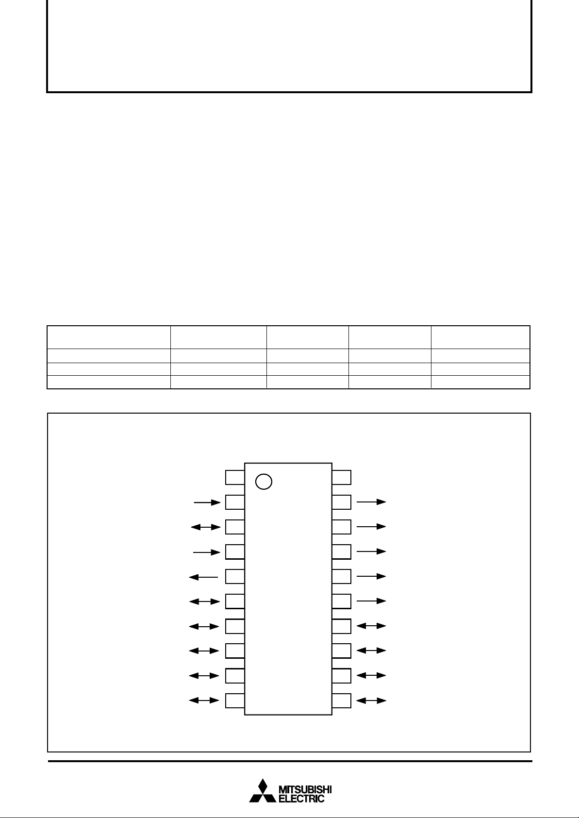
MITSUBISHI MICROCOMPUTERS
4282 Group
SINGLE-CHIP 4-BIT CMOS MICROCOMPUTER
DESCRIPTION
The 4282 Group enables fabrication of 8 × 7 key matrix and has
the followin timers;
• an 8-bit timer which can be used to set each carrier wave and
has two reload register
• an 8-bit timer which can be used to auto-control and has a
reload register.
FEATURES
• Number of basic instructions ............................................. 68
• Minimum instruction execution time ............................ 8.0
(at f(X
IN) = 4.0 MHz, system clock = f(XIN)/8)
• Supply voltage ................................................. 1.8 V to 3.6 V
• Subroutine nesting ..................................................... 4 levels
Product
M34282M1-XXXGP
M34282M2-XXXGP
M34282E2GP
ROM (PROM) size
(× 9 bits)
1024 words
2048 words
2048 words
µ
• Timer
Timer 1 ................................................................... 8-bit timer
(This has a reload register and carrier wave output auto-control
function)
Timer 2 ................................................................... 8-bit timer
(This has two reload registers and carrier wave output function)
• Logic operation function (XOR, OR, AND)
• RAM back-up function
• Key-on wakeup function (ports D
• I/O port (ports D, E, G, CARR) .......................................... 16
• Oscillation circuit .....................................Ceramic resonance
s
• Watchdog timer
• Power-on reset circuit
• Voltage drop detection circuit ......................... Typical:1.50 V
(system reset)
4–D7, E0–E2, G0–G3) .... 11
APPLICATION
Various remote control transmitters
RAM size
(× 4 bits)
48 words
64 words
64 words
Package
20P2E/F-A
20P2E/F-A
20P2E/F-A
ROM type
Mask ROM
Mask ROM
One Time PROM
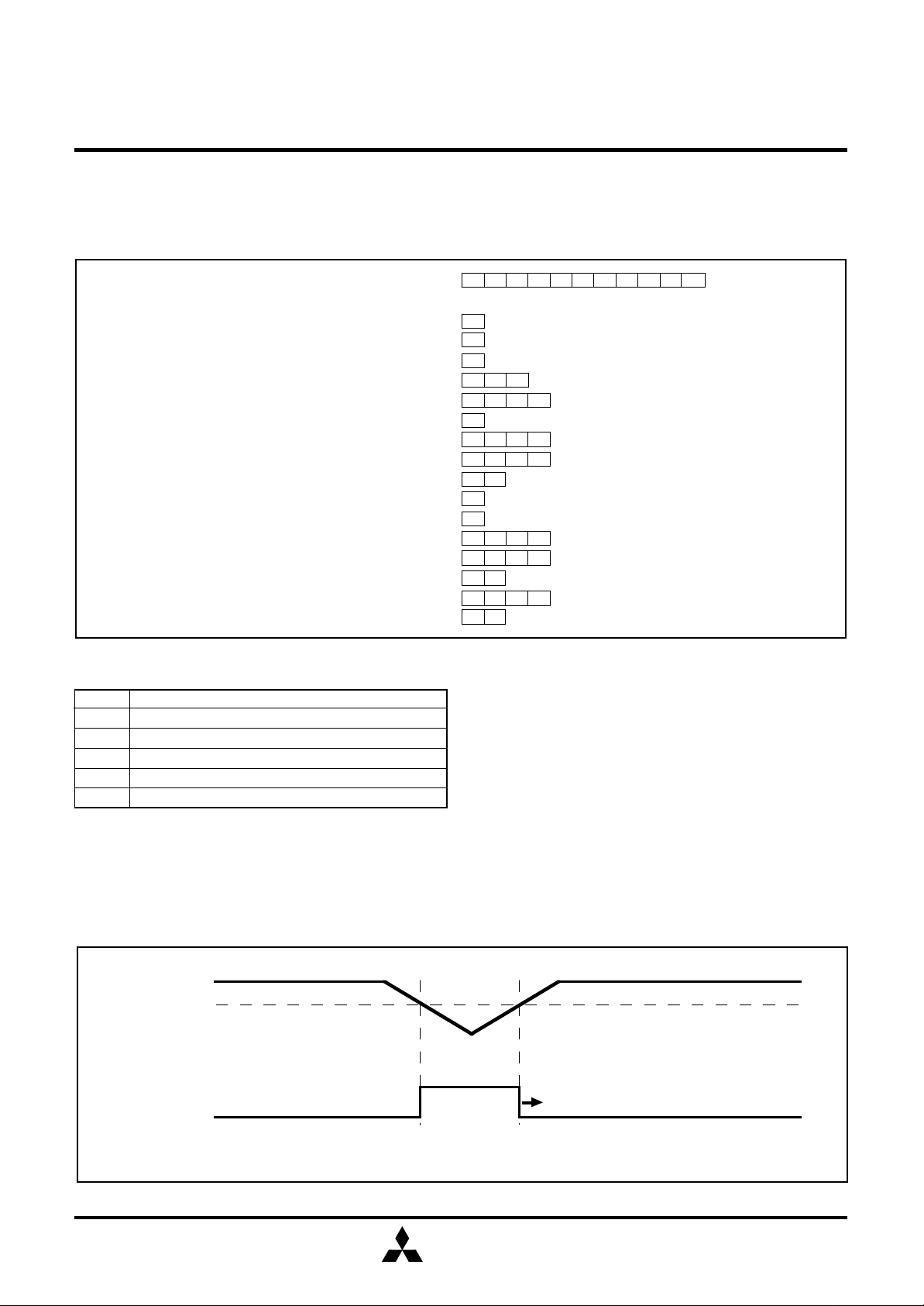
PIN CONFIGURATION (TOP VIEW)
VS
S
E2
E1
XIN
U
XO
T
E0
G0
G1
G2
G3
10
1
2
M
3 4 2 8 2 M x - X X X G
3
4
5
6
7
8
P
9
20
1 9
18
17
1 6
15
1 4
1 3
1 2
1 1
DD
V
CARR
D0
D1
D2
D3
D4
D5
D6
D
7
Outline 20P2E/F-A
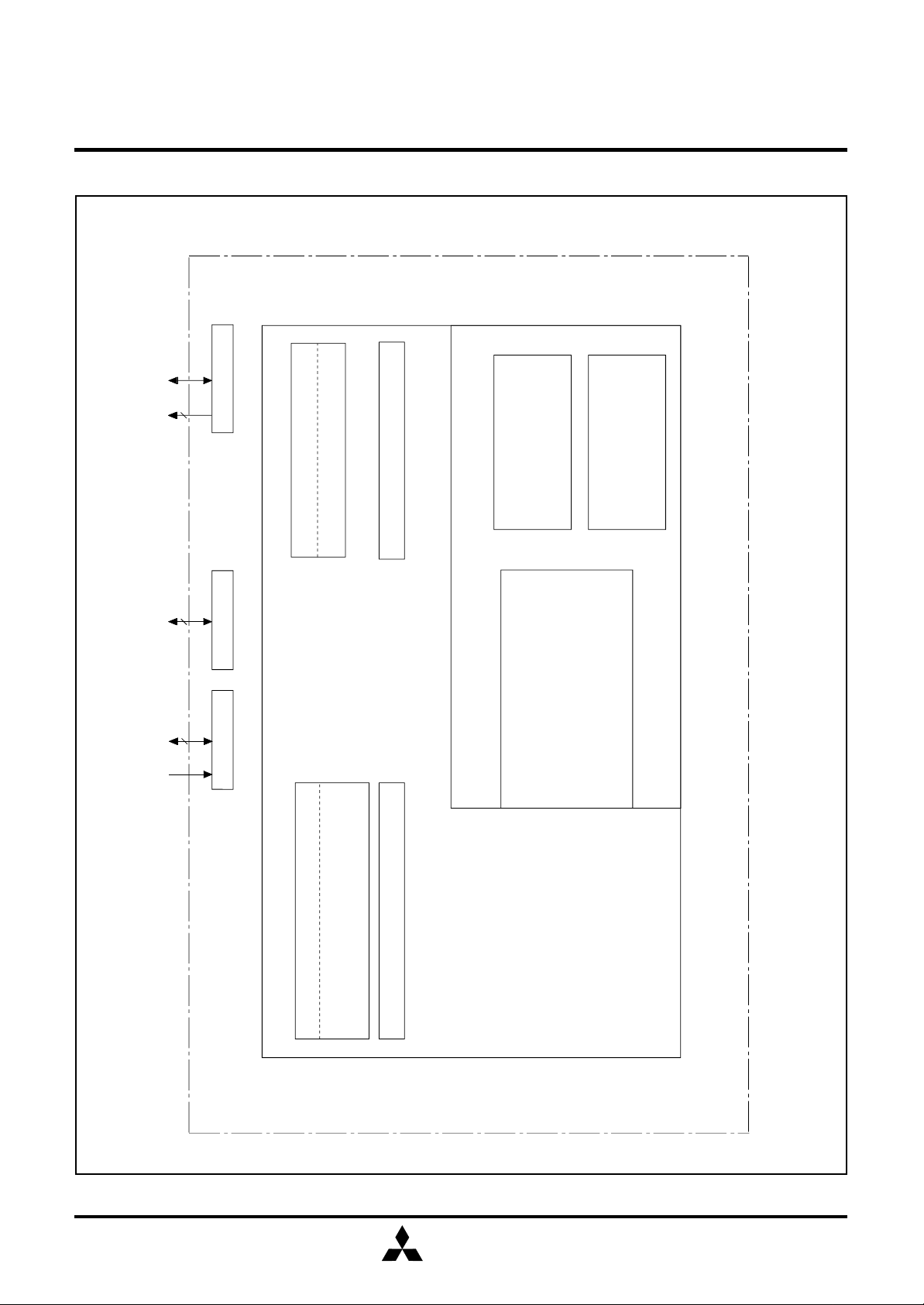
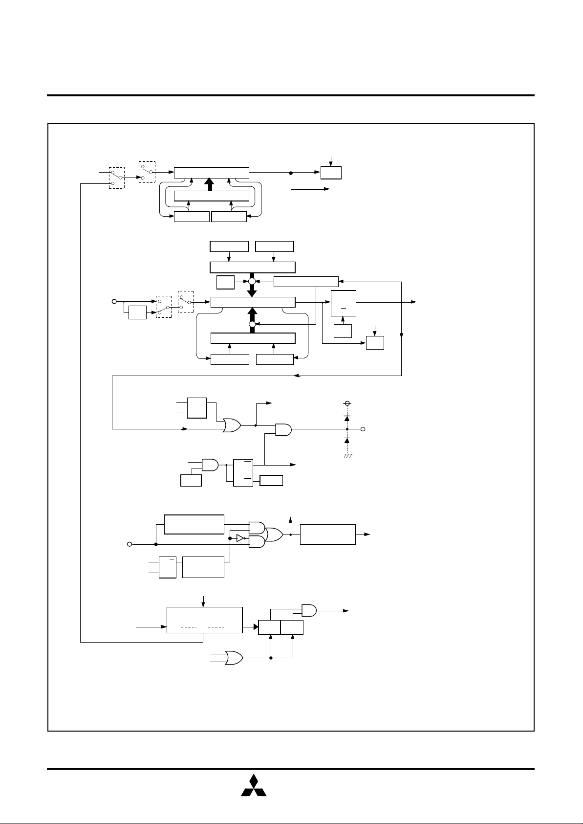
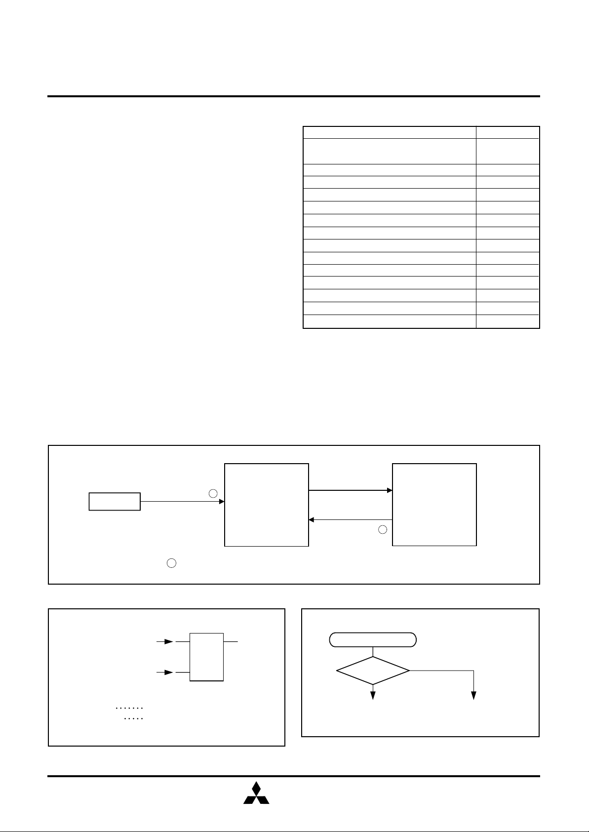
BLOCK DIAGRAM
A
M
( 4 8 , 6 4 w o r d s
✕
4 b i t s
)
R
O
M
( 1 0 2 4 , 2 0 4 8 w o r d s
✕
9 b i t s
)
7
2 0 s e r i e
s
C
P U c o r
e
M
e m o r
y
/
O
p
o
r
t
I
n t e r n a l p e r i p h e r a l f u n c t i o
n
T
i
m
e
r
/
R
e
m
o
t
e
-
c
o
n
t
r
o
l
c
a
r
r
i
e
r
-
w
a
v
e
o
u
t
p
u
t
T
i m e r 1 ( 8 b i t s , c a r r i e r w a v e o u t p u t c o n t r o l
)
T
i m e r 2 ( 8 b i t s , c a r r i e r w a v e g e n e r a t i o n
)
S
y
s
t
e
m
c
l
o
c
k
g
e
n
e
r
a
t
i
o
n
c
i
r
c
u
i
t
X
I
N
-
X
O
U
T
(
N o t e
)
R
e
g
i
s
t
e
r
B
(
4
b
i
t
s
)
R
e
g
i
s
t
e
r
A
(
4
b
i
t
s
)
e
g
i
s
t
e
r
D
(
3
b
i
t
s
)
R
e
g
i
s
t
e
r
E
(
8
b
i
t
s
)
S
t a c k r e g i s t e r S K ( 4 l e v e l s
)
A
L U ( 4 b i t s
)
o
r
t
D
4
o
r
t
G
4
P
o r t
E
2
4
1
W
a t c h d o g t i m e r ( 1 4 b i t s
)
R
e s e t ( v o l t a g e d r o p d e t e c t i o n c i r c u i t
)
N
o
t
e
:
P
R
O
M
2
0
4
8
w
o
r
d
s
✕
9
b
i
t
s
,
R
A
M
6
4
w
o
r
d
s
✕
4
b
i
t
s
f
o
r
b
u
i
l
t
-
i
n
P
R
O
M
v
e
r
s
i
o
n
.
MITSUBISHI MICROCOMPUTERS
4282 Group
SINGLE-CHIP 4-BIT CMOS MICROCOMPUTER
2
MITSUBISHI
ELECTRIC
PERFORMANCE OVERVIEW
Parameter
Number of basic instructions
Minimum instruction execution time
Memory sizes
Input/Output
ports
Timer
Subroutine nesting
Device structure
Package
Operating temperature range
Supply voltage
Power
dissipation
(typical value)
ROM
M34282M2/E2
M34282M1
RAM
M34282M2/E2
M34282M1
0–D3
D
Output
D4–D7
I/O
E0–E2
Input
E0, E1
Output
G0–G3
I/O
CARR
Output
Timer 1
Timer 2
Active mode
RAM back-up mode
MITSUBISHI MICROCOMPUTERS
4282 Group
SINGLE-CHIP 4-BIT CMOS MICROCOMPUTER
Function
68
µ
s (f(XIN) = 4.0 MHz, system clock = f(XIN)/8, VDD = 3 V)
8.0
2048 words ✕ 9 bits
1024 words ✕ 9 bits
64 words ✕ 4 bits
48 words ✕ 4 bits
Four independent output ports
Four independent I/O ports with the pull-down function
3-bit input port with the pull-down function
2-bit output port (E
4-bit I/O port with the pull-down function
1-bit output port; CMOS output
8-bit timer with a reload register
8-bit timer with two reload registers
4 levels (However, only 3 levels can be used when the TABP p instruction is executed)
CMOS silicon gate
20-pin plastic molded SSOP (20P2E/F-A)
–20 °C to 85 °C
1.8 V to 3.6 V
400 µA
IN) = 4.0 MHz, system clock = f(XIN)/8, VDD = 3 V)
(f(X
µ
A (at room temperature, VDD = 3 V)
0.1
0, E1)
PIN DESCRIPTION
Pin
DD
V
VSS
XIN
XOUT
D0–D3
D4–D7
E0–E2
G0–G3
CARR
Name
Power supply
Ground
System clock input
System clock output
Output port D
I/O port D
I/O port E
I/O port G
Carrier wave output
for remote control
Input/Output
—
—
Input
Output
Output
I/O
Output
Input
I/O
Output
Function
Connected to a plus power supply.
Connected to a 0 V power supply.
I/O pins of the system clock generating circuit. Connect a ceramic resonator
between pins X
and XOUT.
Each pin of port D has an independent 1-bit wide output function. The output
structure is P-channel open-drain.
1-bit I/O port. For input use, set the latch of the specified bit to “0.” When the builtin pull-down transistor is turned on, the key-on wakeup function using “H” level
sense and the pull-down transistor become valid. The output structure is P-channel
open-drain.
0, E1) output port. The output structure is P-channel open-drain.
2-bit (E
3-bit input port. For input use (E
When the built-in pull-down transistor is turned on, the key-on wakeup function
using “H” level sense and the pull-down transistor become valid. Port E
input-only port and has a key-on wakeup function using “H” level sense and pulldown transistor.
4-bit I/O port. For input use, set the latch of the specified bit to “0.” The output structure
is P-channel open-drain. When the built-in pull-down transistor is turned on, the keyon wakeup function using “H” level sense and pull-down transistor become valid.
Carrier wave output pin for remote control. The output structure is CMOS circuit.
IN and XOUT. The feedback resistor is built-in between pins XIN
0, E1), set the latch of the specified bit to “0.”
2 has an
MITSUBISHI
ELECTRIC
3
MITSUBISHI MICROCOMPUTERS
4282 Group
SINGLE-CHIP 4-BIT CMOS MICROCOMPUTER
CONNECTIONS OF UNUSED PINS
Pin
0–D7
D
E0, E1
Open or connect to V
Set the output latch to “1” and open, or
connect to V
E2
G0–G3
Open or connect to V
Set the output latch to “1” and open, or
connect to V
Notes 1: Ports D4–D7: Set the bit 2 (PU02) of the pull-down control register PU1 to “0” by software and turn the pull-down transistor
OFF.
2: Set the corresponding bits of the pull-down control register PU0 to “0” by software and turn the pull-down transistor OFF.
(Note in order to set the output latch to “1” to make pins open)
• After system is released from reset, a port is in a high-impedance state until the output latch of the port is set to “1” by software.
Accordingly, the voltage level of pins is undefined and the excess of the supply current may occur.
• To set the output latch periodically is recommended because the value of output latch may change by noise or a program run away
(caused by noise).
Connection
DD pin (Note 1).
DD pin (Note 2).
SS pin.
DD pin (Note 2).
(Note when connecting to V
SS and VDD)
• Connect the unused pins to V
PORT FUNCTION
Port
Port D
Port E
Port G
Port CARR
0–D3
D
D4–D7
E0
E1
E2
G0–G3
CARR
Pin
SS or VDD at the shortest distance and use the thick wire against noise.
Input/
Output
Output
(4)
Output structure
P-channel open-drain
Control
bits
1 bit
Control
instructions
SD
RD
Control
registers
CLD
I/O
(4)
SD
RD
PU1
CLD
SZD
I/O
P-channel open-drain
(2)
Output:
2 bits
OEA
IAE
PU0
Input:
Input
3 bits
IAE
(1)
I/O
(4)
Output
(1)
P-channel open-drain
CMOS
4 bits
1 bit
OGA
IAG
SCAR
RCAR
PU0
Remark
Pull-down function and
key-on wakeup function
(programmable)
Pull-down function and
key-on wakeup function
(programmable)
Pull-down function and
key-on wakeup function
(programmable)
DEFINITION OF CLOCK AND CYCLE
• System clock (STCK)
The system clock is the source clock for controlling this product.
It can be selected as shown below whether to use the CCK
instruction.
CCK instruction
When not using
When using
4
System clock
f(X
IN)/8
IN)
f(X
Instruction clock
IN)/32
f(X
IN)/4
f(X
• Instruction clock (INSTCK)
The instruction clock is a signal derived by dividing the system
clock by 4, and is the basic clock for controlling CPU. The one
instruction clock cycle is equivalent to one machine cycle.
• Machine cycle
The machine cycle is the cycle required to execute the
instruction.
MITSUBISHI
ELECTRIC
PORT BLOCK DIAGRAMS
MITSUBISHI MICROCOMPUTERS
4282 Group
SINGLE-CHIP 4-BIT CMOS MICROCOMPUTER
SD instruction
RD instruction
SD instruction
RD instruction
Skip decision (SZD instruction)
Register A
A
(Note 3)
A
Key-on wakeup input
Register A
A
(Note 3)
Key-on wakeup input
Register Y
CLD instruction
DecoderRegister Y
CLD instruction
Key-on wakeup
j
OEA
instruction
j
Register A
Key-on wakeup input
j
OGA
instruction
A
j
D
T
A
2
D
T
Decoder
Q
IAE instruction
Q
IAG instruction
S
Q
R
(Note 2)
(Note 3)
IAE instruction
PU1
PU0
PU0
S
Q
R
i
j
2
(Note 1)
(Note 1)
Pull-down transistor
(Note 1)
Pull-down
transistor
Pull-down
transistor
Pull-down transistor
(Note 1)
(Note 1)
Ports D0–D3
Ports D4–D7 (Note 5)
Ports E0, E1 (Note 5)
Port E2 (Note 5)
Ports G0, G1 (Note 5)
Register A
k
A
(Note 4)
instruction
A
k
Key-on wakeup input
SCAR instruction
RCAR instruction
(from timer 2)
Timer 1 underflow signal
OGA
CARRYD
Q
D
T
CAR flag
V1
IAG instruction
SRQ
2
(Note 1)
Ports G2, G3 (Note 5)
Pull-down transistor
PU0
3
CARRY
(to timer 1)
(Note 1)
Port CARR
Q
D
V1
R
T
Carrier wave output control signal
0
Notes 1:
This symbol represents a parasitic diode.
2: i represents bits 0 to 3.
3: j represents bits 0, 1.
4: k represents bits 2, 3.
5: Applied voltage must be less than VDD.
MITSUBISHI
ELECTRIC
5

FUNCTION BLOCK OPERATIONS
CPU
(1) Arithmetic logic unit (ALU)
The arithmetic logic unit ALU performs 4-bit arithmetic such
as 4-bit data addition, comparison, and bit manipulation.
MITSUBISHI MICROCOMPUTERS
4282 Group
SINGLE-CHIP 4-BIT CMOS MICROCOMPUTER
<Carry>
(CY)
(M(DP))
Addition
ALU
(2) Register A and carry flag
Register A is a 4-bit register used for arithmetic, transfer,
exchange, and I/O operation.
Carry flag CY is a 1-bit flag that is set to “1” when there is a
carry with the AMC instruction (Figure 1).
It is unchanged with both A n instruction and AM instruction.
The value of A
instruction (Figure 2).
Carry flag CY can be set to “1” with the SC instruction and
cleared to “0” with the RC instruction.
(3) Registers B and E
Register B is a 4-bit register used for temporary storage of 4bit data, and for 8-bit data transfer together with register A.
Register E is an 8-bit register. It can be used for 8-bit data
transfer with register B used as the high-order 4 bits and
register A as the low-order 4 bits (Figure 3).
(4) Register D
Register D is a 3-bit register.
It is used to store a 7-bit ROM address together with register
A and is used as a pointer within the specified page when the
TABP p, BLA p, or BMLA p instruction is executed (Figure 4).
0 is stored in carry flag CY with the RAR
(A)
<Result>
Fig. 1 AMC instruction execution example
<Set>
SC instruction
<Clear>
RC instruction
CY A3A2A1A
<Rotation>
RAR instruction
A
0
CY A3A2A
Fig. 2 RAR instruction execution example
Register B Register A
B3B2B1B
TAB instruction
0
A3A2A1A
TEAB instruction
Register E
ER7ER6ER5ER4ER3ER2ER1ER
0
1
0
0
TABP p instruction
Specifying address
PC
H
p3p2p1p
Immediate field
value p
Fig. 4 TABP p instruction execution example
0
DR2DR1DR
The contents
of register D
PC
A3A2A1A
0
The contents
of register A
TABE instruction
B3B2B1B
Register B Register A
Fig. 3 Registers A, B and register E
0
A3A2A1A
TBA instruction
0
ROM
8
40
Low-order 4 bits
L
0
Middle-order 4 bits
Register A (4)
Register B (4)
Most significant 1 bit
Carry flag CY (1)
URS flag (1)
URSC instruction
6
ELECTRIC
MITSUBISHI
(5) Most significant ROM code reference enable flag (URS)
URS flag controls whether to refer to the contents of the most
significant 1 bit (bit 8) of ROM code when executing the TABP
p instruction. If URS flag is “0,” the contents of the most
significant 1 bit of ROM code is not referred even when
executing the TABP p instruction. However, if URS flag is “1,”
the contents of the most significant 1 bit of ROM code is set to
flag CY when executing the TABP p instruction (Figure 4).
URS flag is “0” after system is released from reset and returned
from RAM back-up mode. It can be set to “1” with the URSC
instruction, but cannot be cleared to “0.”
(6) Stack registers (SKs) and stack pointer (SP)
Stack registers (SKs) are used to temporarily store the contents
of program counter (PC) just before branching until returning
to the original routine when;
• performing a subroutine call, or
• executing the table reference instruction (TABP p).
Stack registers (SKs) are four identical registers, so that
subroutines can be nested up to 4 levels. However, one of
stack registers is used when executing a table reference
instruction. Accordingly, be careful not to over the stack. The
contents of registers SKs are destroyed when 4 levels are
exceeded.
The register SK nesting level is pointed automatically by 2-bit
stack pointer (SP).
Figure 5 shows the stack registers (SKs) structure.
Figure 6 shows the example of operation at subroutine call.
(7) Skip flag
Skip flag controls skip decision for the conditional skip
instructions and continuous described skip instructions.
Note : The 4282 Group just invalidates the next instruction
when a skip is performed. The contents of program
counter is not increased by 2. Accordingly, the number
of cycles does not change even if skip is not performed.
However, the cycle count becomes “1” if the TABP p,
RT, or RTS instruction is skipped.
MITSUBISHI MICROCOMPUTERS
4282 Group
SINGLE-CHIP 4-BIT CMOS MICROCOMPUTER
Program counter (PC)
SK
SK
SK
SK
0
1
2
3
(SP) ← 0
(SK
(PC) ← SUB1
Executing RT
instruction
0
is destroyed.
0
) ← 0001
16
(PC) ← (SK0)
(SP) ← 3
(SP) = 0
(SP) = 1
(SP) = 2
(SP) = 3
Subroutine
SUB1 :
Executing BM
instruction
Stack pointer (SP) points “3” at reset or
returning from RAM back-up mode. It points “0”
by executing the first BM instruction, and the
contents of program counter is stored in SK
When the BM instruction is executed after four
stack registers are used ((SP) = 3), (SP) = 0
and the contents of SK
Fig. 5 Stack registers (SKs) structure
Main program
Address
0000
16
NOP
16
BM SUB1
0001
000216 NOP
NOP
RT
0
.
·
·
·
Returning to the BM instruction execution
Note:
address with the RT instruction, and the BM
instruction is equivalent to the NOP instruction.
Fig. 6 Example of operation at subroutine call
MITSUBISHI
ELECTRIC
7
MITSUBISHI MICROCOMPUTERS
4282 Group
SINGLE-CHIP 4-BIT CMOS MICROCOMPUTER
(8) Program counter (PC)
Program counter (PC) is used to specify a ROM address (page
and address). It determines a sequence in which instructions
stored in ROM are read. It is a binary counter that increments
the number of instruction bytes each time an instruction is
executed. However, the value changes to a specified address
when branch instructions, subroutine call instructions, return
instructions, or the table reference instruction (TABP p) is
executed.
Program counter consists of PC
which specifies to a ROM page and PC
H (most significant bit to bit 7)
L (bits 6 to 0) which
specifies an address within a page. After it reaches the last
address (address 127) of a page, it specifies address 0 of the
next page (Figure 7).
Make sure that the PC
H does not exceed after the last page of
the built-in ROM.
(9) Data pointer (DP)
Data pointer (DP) is used to specify a RAM address and
consists of registers X and Y. Register X specifies a file and
register Y specifies a RAM digit (Figure 8).
Register Y is also used to specify the port D bit position.
When using port D, set the port D bit position to register Y
certainly and execute the SD, RD, or SZD instruction (Figure
9).
Program counter (PC)
p3p2p1p0a6a5a4a3a2a1a
PC
H
Specifying
PC
L
Specifying address
page
Fig. 7 Program counter (PC) structure
Data pointer (DP)
X1X0Y3Y2Y1Y
Register Y (4)
Register X (2)
0
Specifying RAM file
0
Specifying
RAM digit
Fig. 8 Data pointer (DP) structure
Specifying bit position
Set
D
5
7
1
Port D output latch
1
01
0
Register Y (4)
D
Fig. 9 SD instruction execution example
D
0
8
ELECTRIC
MITSUBISHI

PROGRAM MEMORY (ROM)
The program memory is a mask ROM. 1 word of ROM is
composed of 9 bits. ROM is separated every 128 words by the
unit of page (addresses 0 to 127).
Table 1 ROM size and pages
Product
M34282M2/E2
M34282M1
ROM size (✕ 9 bits)
2048 words
1024 words
Pages
16 (0 to 15)
8 (0 to 7)
MITSUBISHI MICROCOMPUTERS
4282 Group
SINGLE-CHIP 4-BIT CMOS MICROCOMPUTER
087654321
16
0000
F
16
007
008016
00
FF
16
010016
017
F
16
018016
Subroutine special page
Page 0
Page 1
Page 2
Page 3
Page 2 (addresses 0100
subroutine calls. Subroutines written in this page can be called
from any page with the 1-word instruction (BM). Subroutines
extending from page 2 to another page can also be called with
the BM instruction when it starts on page 2.
ROM pattern of all addresses can be used as data areas with
the TABP p instruction.
16 to 017F16) is the special page for
DATA MEMORY (RAM)
1 word of RAM is composed of 4 bits, but 1-bit manipulation
(with the SB j, RB j, and SZB j instructions) is enabled for the
entire memory area. A RAM address is specified by a data
pointer. The data pointer consists of registers X and Y. Set a
value to the data pointer certainly when executing an instruction
to access RAM.
Table 2 shows the RAM size. Figure 11 shows the RAM map.
Table 2 RAM size
Product
M34282M2/E2
M34282M1
64 words ✕ 4 bits (256 bits)
48 words ✕ 4 bits (192 bits)
RAM size
07
FF
16
Fig. 10 ROM map of M34282M2/E2
RAM 64 words ✕ 4 bits (256 bits)
Register X
0
1
0
1
2
3
4
5
6
7
8
Register Y
9
10
11
12
13
14
15
Page 15
23
48 words
M34282M1
Fig. 11 RAM map
MITSUBISHI
ELECTRIC
64 words
M34282M2/E2
9
TIMERS
The 4282 Group has the programmable timer.
• Programmable timer
The programmable timer has a reload register and enables
the frequency dividing ratio to be set. It is decremented from a
setting value n. When it underflows (count to n + 1), a timer 1
underflow flag is set to “1,” new data is loaded from the reload
register, and count continues (auto-reload function).
FF
16
n: Counter initial value
Count starts
n
1st underflow 2nd underflow
MITSUBISHI MICROCOMPUTERS
4282 Group
SINGLE-CHIP 4-BIT CMOS MICROCOMPUTER
Reload Reload
The contents of counter
00
16
n+1 count n+1 count
Timer 1 underflow flag
“1”
“0”
Fig. 12 Auto-reload function
The 4282 Group timer consists of the following circuit.
• Timer 1 : 8-bit programmable timer
• Timer 2 : 8-bit programmable timer
These timers can be controlled with the timer control registers
V1 and V2.
Each timer function is described below.
Table 3 Function related timer
Circuit
Timer 1
Timer 2
14-bit timer
Structure
8-bit programmable
binary down counter
8-bit programmable
binary down counter
14-bit fixed frequency
Count source
• Carrier wave output (CARRY)
• Bit 5 of watchdog timer
IN)
• f(X
IN)/2
• f(X
• Instruction clock
Frequency
dividing ratio
1 to 256
1 to 256
16384
A skip instruction is executed
Use of output signal
• Carrier wave output control
• Carrier wave output
• Watchdog timer
• Timer 1 count source
Time
Control
register
V1
V2
10
MITSUBISHI
ELECTRIC
MITSUBISHI MICROCOMPUTERS
4282 Group
SINGLE-CHIP 4-BIT CMOS MICROCOMPUTER
CARRY
V1
X
IN
V1
0
1
0
1
0
1
(TAB1)
1/2
SCAR instruction
RCAR instruction
(Note 1)
Reload register R1 (8)
(T1AB)
Register B Register A
V2
0 (Note 1)
V2
1
0
0
1
1
(TAB2)
CAR flag
SQ
R
Timer 1 (8)
(Note 2)
Register B
Reload register R2H (8)
3
V2
(T2R2L)
(Note 3)
(T2AB)
Reload register R2L (8)
Register B
(T2HAB)
Timer 2(8)
(T2AB)
(TAB1)
Register A
Reload control circuit
Register A
CARRY
(to timer 1)
SNZT1 instruction
T1F
Timer 1 underflow signal
(to port CARR)
T
R
V2
2
(TAB2)
Q
SNZT2
instruction
T2F
T2F
Port CARR
CARRYD
(to port CARR)
Timer 1 underflow signal
X
IN
CCK instruction
Initializing signal
(Note 3)
INSTCK
Fig. 13 Timers structure
V1
2
Frequency divider
(divided by 8)
Synchronous
QS
circuit
R
Initializing signal
14-bit timer (WDT)
WRST instruction
Initializing signal
(Note 4)
DTQ
V1
R
(Note 4)
5
130
WDF1 WDF2
Carrier wave output control signal
0
STCK (System clock)
Frequency divider
(divided by 4)
Notes 1: Counting is stopped by clearing to “0.”
2: When the T1AB instruction is executed after V1
writing is performed only to reload register R1.
3: The data of reload register R2L set with the T2AB instruction
can be also written to timer 2 with the T2R2L instruction.
4: The initializing signal is output at reset or RAM back-up mode.
INSTCK
(Instruction clock)
System reset
0
is set to “1,”
MITSUBISHI
ELECTRIC
11
Table 4 Control registers related to timer
MITSUBISHI MICROCOMPUTERS
4282 Group
SINGLE-CHIP 4-BIT CMOS MICROCOMPUTER
Timer control register V1
2
V1
V11
V10
V13
V12
V11
V10
Note: “W” represents write enabled.
(1) Control registers related to timer
• Timer control register V1
• Timer control register V2
Carrier wave output auto-control bit
Timer 1 count source selection bit
Timer 1 control bit
Timer control register V1
Carrier wave “H” interval expansion bit
Carrier wave generation function control bit
Timer 2 count source selection bit
Timer 2 control bit
Register V1 controls the timer 1 count source and autocontrol function of carrier wave output from port CARR by
timer 1. Set the contents of this register through register A
with the TV1A instruction.
Register V2 controls the timer 2 count source and the carrier
wave generation function by timer. Set the contents of this
register through register A with the TV2A instruction.
at reset : 0002 Wat RAM back-up : 0002
Auto-control output by timer 1 is invalid
0
Auto-control output by timer 1 is valid
1
Carrier wave output (CARRY)
0
Bit 5 of watchdog timer (WDT)
1
Stop (Timer 1 state retained)
0
Operating
1
at reset : 00002 Wat RAM back-up : 00002
To expand “H” interval is invalid
0
To expand “H” interval is valid (when V2
1
Carrier wave generation function invalid
0
Carrier wave generation function valid
1
IN)
f(X
0
IN)/2
f(X
1
Stop (Timer 2 state retained)
0
Operating
1
2=1 selected)
(2) Precautions
Note the following for the use of timers.
• Count source
Stop timer 1 or timer 2 counting to change its count source.
• Watchdog timer
Be sure that the timing to execute the WRST instruction in
order to operate WDT efficiently.
• Writing to reload register R1
When writing data to reload register R1 while timer 1 is
operating, avoid a timing when timer 1 underflows.
• Timer 1 count operation
When the bit 5 of the watchdog timer (WDT) is selected as
the timer 1 count source, the error of maximum ± 256 µs
(at the minimum instruction execution time : 8 µs) is
generated from timer 1 start until timer 1 underflow. When
programming, be careful about this error.
• Stop of timer 2
Avoid a timing when timer 2 underflows to stop timer 2.
• Writing to reload register R2H
When writing data to reload register R2H while timer 2 is
operating, avoid a timing when timer underflows.
• Timer 2 carrier wave output function
When to expand “H” interval of carrier wave is valid, set “1”
or more to reload register R2H.
12
MITSUBISHI
ELECTRIC

MITSUBISHI MICROCOMPUTERS
4282 Group
SINGLE-CHIP 4-BIT CMOS MICROCOMPUTER
(3) Timer 1
Timer 1 is an 8-bit binary down counter with the timer 1 reload
register (R1).
When timer is stopped, data can be set simultaneously in timer
1 and the reload register (R1) with the T1AB instruction.
When timer is operating, data can be set to only reload register
R1 with the T1AB instruction.
When setting the next count data to reload register R1 at
operating, set data before timer 1 underflows.
Timer 1 starts counting after the following process;
➀ set data in timer 1,
➁ select the count source with the bit 1 of register V1, and
➂ set the bit 0 of register V1 to “1.”
Once count is started, when timer 1 underflows (the next count
pulse is input after the contents of timer 1 becomes “0”), the
timer 1 underflow flag (T1F) is set to “1,” new data is loaded
from reload register R1, and count continues (auto-reload
function).
When a value set in reload register R1 is n, timer 1 divides the
count source signal by n + 1 (n = 0 to 255).
When the bit 2 of register V1 is set to “1,” the carrier wave
output enable/disable interval of port CARR is alternately
generated each timer 1 underflows (Figure 14).
Data can be read from timer 1 to registers A and B. When
reading the data, stop the counter and then execute the TAB1
instruction.
(4) Timer 2
Timer 2 is an 8-bit binary down counter with the timer 2 reload
registers (R2H and R2L).
Data can be set simultaneously in timer 2 and the reload
register (R2L) with the T2AB instruction.
The contents of reload register (R2L) set with the T2AB
instruction can be set again to timer 2 with the T2R2L
instruction. Data can be set to reload register (R2H) with the
T2HAB instruction.
Timer 2 starts counting after the following process;
➀ set data in timer 2,
➁ select the count source with the bit 1 of register V2, and
➂ select the valid/invalid of the carrier wave generation
function by bit 2 of register V1 (when this function is valid,
select the valid/invalid of the carrier wave “H” interval
expansion by bit 3), and
➃ set the bit 0 of register V1 to “1.”
When the carrier wave generation function is invalid (V2
the following operation is performed;
Once count is started, when timer 2 underflows (the next count
pulse is input after the contents of timer 2 becomes “0”), the
timer 2 underflow flag (T2F) is set to “1,” new data is loaded
from reload register R2L, and count continues (auto-reload
function).
When a value set in reload register R2L is n, timer 2 divides
the count source signal by n + 1 (n = 0 to 255).
When the carrier wave generation function is valid (V2
the carrier wave which has the “L” interval set to the reload
register R2L and “H” interval set to the reload register R2H
can be output (Figure 15).
After the count of the “L” interval of carrier wave is started,
timer 2 underflows and the timer 2 underflow flag (T2F) is set
2=“0”),
2=“1”),
to “1”. Then, the “H” interval data of carrier wave is reloaded
from the reload register R2H, and count continues.
When timer underflows again after auto-reload, the T2F flag
is set to “1”. And then, the “L” interval data of carrier wave is
reloaded from the reload register R2L, and count continues.
After that, each timer underflows, data is reloaded from reload
register R2H and R2L alternately.
When a value set in reload register R2H is n, “H” interval of
carrier wave is as follows;
➀ When to expand “H” interval is invalid (V2
Count source ✕ (n+1), n = 0 to 255
➁ When to expand “H” interval is valid (V2
Count source ✕ (n+1.5), n = 1 to 255
When a value set in reload register R2L is m, “L” interval of
carrier wave is as follows;
Count source ✕ (m+1), m = 0 to 255
Data can be read from timer 2 to registers A and B. When
reading the data, stop the counter and then execute the TAB2
instruction.
(5) Timer underflow flags (T1F, T2F)
Timer 1 underflow flag or timer 2 underflow flag is set to “1”
when the timer 1 or timer 2 underflows. The state of flags T1F
and T2F can be examined with the skip instruction (SNZT1,
SNZT2).
Flags T1F and T2F are cleared to “0” when the next instruction
is skipped with a skip instruction.
3 = “0”),
3 = “1”),
MITSUBISHI
ELECTRIC
13

T i m e r 1 u n d e r f l o w
Port CARR output
S e t t h e i n t e r v a l “ a ” t o t i m e r 1 .
C o u n t s o u r c e C A R R Y s e l e c t e d
T i m e r 1 u n d e r f l o w
C A R R Y
Port CARR output
R e g i s t e r V 1
T i m e r 1 s t a r t s
“1”
“0”
“ H ”
“L”
▲▲ ▲ ▲
( V 11)←0
A u t o - c o n t r o l v a l i d
( V 12)←1
“ 1 ”
“ 0 ”
“H”
“ L ”
“H”
“ L ”
“ 1 ”
2
“ 0 ”
C a r r i e r w a v e o u t p u t s t a r t
(V10)←1
a b c
S e t t h e i n t e r v a l “ b ”
t o r e l o a d r e g i s t e r R 1 .
Carrier wave output start
SINGLE-CHIP 4-BIT CMOS MICROCOMPUTER
Set the interval “c”
to reload register R1.
A u t o - c o n t r o l i n v a l i dAuto-control invalid
MITSUBISHI MICROCOMPUTERS
4282 Group
d
Set the interval “d”
to reload register R1.
T i m e r 1 s t o p
( V 10)←0
( N o t e )
Carrier wave output stop
N o t e : W h e n t i m e r 1 i s s t o p p e d , t h e p o r t C A R R o u t p u t a u t o - c o n t r o l i s t e r m i n a t e d r e g a r d l e s s o f b i t 2 ( V 12) o f r e g i s t e r V 1 .
Fig. 14 Port CARR output control by timer 1
● I n t h i s c a s e , t h e f o l l o w i n g i s s e t ;
• T i m e r 2 c a r r i e r w a v e g e n e r a t i o n f u n c t i o n i s v a l i d ( V 2
• “ L ” i n t e r v a l ( 0 3
• “ H ” i n t e r v a l ( 0 2
T o e x p a n d “ H ” i n t e r v a l o f c a r r i e r w a v e i s i n v a l i d ( V 23= “ 0 ” )
[ C o u n t s o u r c e : 4 . 0 M H z , R e s o l u t i o n : 2 5 0 n s ]
T i m e r 2 c o u n t s o u r c e
T i m e r 2 c o u n t v a l u e
(Reload register)
T i m e r 2 u n d e r f l o w s i g n a l
T o e x p a n d “ H ” i n t e r v a l o f c a r r i e r w a v e i s v a l i d ( V 23= “ 1 ” )
(W h e n c o u n t s o u r c e i s 4 . 0 M H z , c a r r i e r w a v e i s e x p a n d e d f o r 1 2 5 n s ]
T i m e r 2 c o u n t s o u r c e
T i m e r 2 c o u n t v a l u e
( R e l o a d r e g i s t e r )
T i m e r 2 u n d e r f l o w s i g n a l
C A R R Y D
1 6
) o f c a r r i e r w a v e i s s e t t o r e l o a d r e g i s t e r R 2 L
1 6
) o f c a r r i e r w a v e i s s e t t o r e l o a d r e g i s t e r R 2 H
0 2
1 6
0 1
0 3
1 6
(R2L)
T i m e r 2 s t a r t s
0 3
1 6
(R2L)
1 6
0 2
1 6
0 1
1 60016
2
= “ 1 ” ) ,
0 2
1 60116
0 0
03
0 0
1 6
0 2
1 6
0 1
1 6
( R 2 H ) (R2L) (R2H) (R2L) ( R 2 H )
3 c l o c k s
i n t e r v a l
C a r r i e r w a v e p e r i o d :
0 2
1 6
0 1
( R 2 H )
16
0 0
1 6
7 c l o c k s
02160 1
0 3
1 6
1 6
0 0
1 6
( R 2 L ) (R2H) ( R 2 L ) ( R 2 H )
1 6
1 60016
021601160 0
3 clocks
interval
C a r r i e r w a v e p e r i o d :
02160 1
03
1 6
7 c l o c k s
1 6
0 0
16
1 6
02160 1
03
16
1 6
0 2
1 6
0 0
1 6
02160 1
1 6
0 1
1 6
0 0
1 6
0 2
1 6
C A R R Y D
T i m e r 2 s t a r t s
N o t e : W h e n t o e x p a n d “ H ” i n t e r v a l o f t h e c a r r i e r w a v e i s v a l i d , s e t “ 0 1
Fig. 15 Carrier wave generation example by timer 2
14
3 . 5 c l o c k s
i n t e r v a l
C a r r i e r w a v e p e r i o d :
7 . 5 c l o c k s
1 6
MITSUBISHI
ELECTRIC
3 . 5 c l o c k s
i n t e r v a l
C a r r i e r w a v e p e r i o d :
” o r m o r e t o r e l o a d r e g i s t e r R 2 H .
7 . 5 c l o c k s
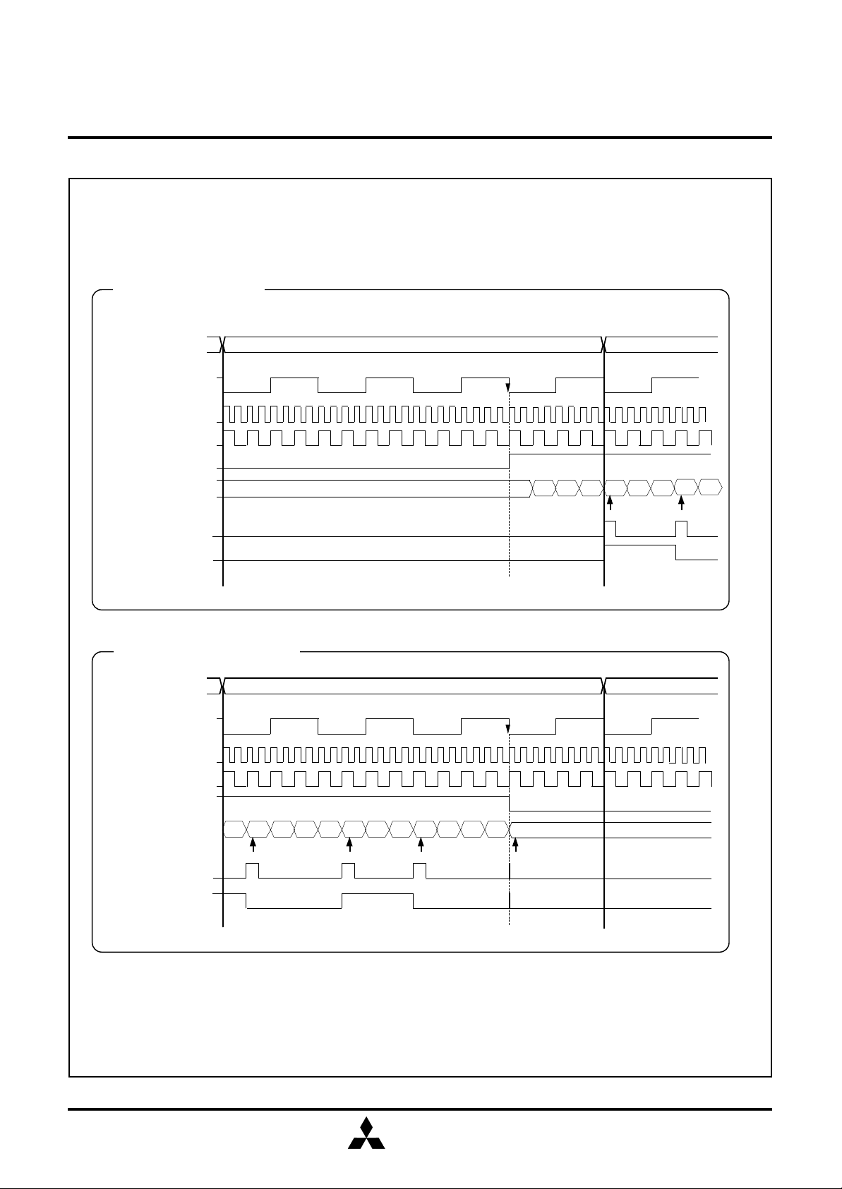
● In this case, the following is set;
• To expand “H” interval of carrier wave is invalid (V2
• Timer 2 carrier wave generation function is valid (V2
• Count source X
• “L” interval (03
• “H” interval (02
IN
/2 selected (V21=“1”),
16
) of carrier wave is set to reload register R2L
16
) of carrier wave is set to reload register R2H
Timer 2 count start timing
3
= “0”),
2
=“1”),
MITSUBISHI MICROCOMPUTERS
4282 Group
SINGLE-CHIP 4-BIT CMOS MICROCOMPUTER
Machine cycle
Instruction clock
(Count source selected)
Timer 2 count value
(Reload register)
Timer 2 underflow signal
IN
=f(X
XIN/2
Register V2
CARRYD
Timer 2 count stop timing
Machine cycle
Instruction clock
=f(X
(Count source selected)
Timer 2 count value
(Reload register)
Timer 2 underflow signal
XIN/2
Register V2
Mi Mi + 1 Mi + 2
TV2A instruction execution cycle (V20) ←1
)/8
X
IN
0
03
(R2L)
16
0216011600
0216011600
16
(R2H) (R2L)
Timer 2 count start timing
Mi Mi + 1 Mi + 2
TV2A instruction execution cycle (V20)←0
IN
)/8
X
IN
0
02
00
02160116001602160116001603
16
03
16
(R2H)(R2L)
0216011600
16
16
16
(R2H)(R2L)
16
02
16
03
16
CARRYD
Notes 1: When the carrier wave generation function is vaild (V2
when timer 2 underflows to stop timer 2. When the timer 2 count stop occurs
at the same timing with the timer 2 underflows, hazard may occur in the carrier
wave output waveform.
2: When the timer 2 is stopped during “H” output of carrier wave while the carrier
wave generation function is valid, it is stopped after the “H” interval set by
reload register R2H is output.
Fig. 16 Timer 2 count start/stop timing
Timer 2 count stop timing
MITSUBISHI
ELECTRIC
(Note 1)
2
=“1”), avoid a timing
15

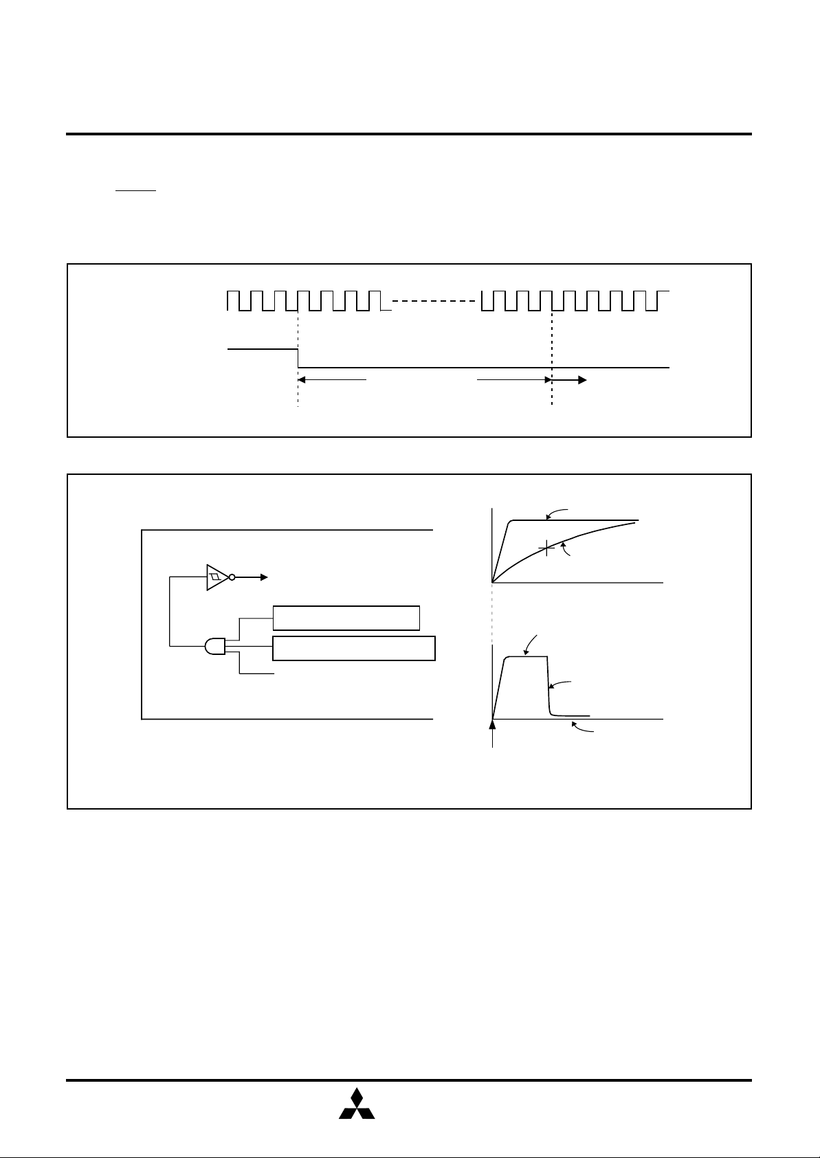
WATCHDOG TIMER
S
Sof
S
Watchdog timer provides a method to reset and restart the system
when a program runs wild. Watchdog timer consists of 14-bit
timer (WDT) and watchdog timer flags (WDF1, WDF2).
Watchdog timer downcounts the instruction clock (INSTCK) as
the count source immediately after system is released from reset.
When the timer WDT count value becomes 0000
occurs, the WDF1 flag is set to “1.” Then, when the WRST
instruction is not executed before the timer WDT counts 16383,
WDF2 flag is set to “1” and internal reset signal is generated and
system reset is performed.
Execute the WRST instruction at period of 16383 machine cycle
or less to keep the microcomputer operation normal.
Timer WDT is also used for generation of oscillation stabilization
time. When system is returned from reset and from RAM backup mode by key-input, software starts after the stabilization
oscillation time until timer WDT downcounts to 3E00
16 and underflow
16 elapses.
MITSUBISHI MICROCOMPUTERS
4282 Group
SINGLE-CHIP 4-BIT CMOS MICROCOMPUTER
3 F F F
3 E 0 0
1 6
1 6
o f t w a r e s t a r
t
tware start
Value of timer WDT
0 0 0 0
1 6
W D F 1 f l a g
WDF2 flag
“1”
“ 0 ”
“ 1 ”
“0”
I n t e r n a l r e s e t s i g n a l
“H”
“L”
POF
instruction
execution
S y s t e m
Return
r e s e t
Fig. 17 Watchdog timer function
LOGIC OPERATION FUNCTION
The 4282 Group has the 4-bit logic operation function. The logic
operation between the contents of register A and the low-order
4 bits of register E is performed and its result is stored in register
A.
Table 5 Logic operation selection register LO
WRST
instruction
o f t w a r e s t a r
S y s t e m
r e s e t
t
execution
Each logic operation can be selected by setting logic operation
selection register LO.
Set the contents of this register through register A with the TLOA
instruction. The logic operation selected by register LO is
executed with the LGOP instruction.
Table 5 shows the logic operation selection register LO.
Logic operation selection register LO
LO1
Logic operation selection bits
LO0
Note: “W” represents write enabled.
16
at reset : 002
LO1
0
LO
0
0
0
1
1
0
1
1
MITSUBISHI
ELECTRIC
at RAM back-up : 002
Logic operation function
Exclusive logic OR operation (XOR)
OR operation (OR)
AND operation (AND)
Not available
W
MITSUBISHI MICROCOMPUTERS
4282 Group
SINGLE-CHIP 4-BIT CMOS MICROCOMPUTER
RESET FUNCTION
The 4282 Group has the power-on reset circuit, though it does
not have RESET pin. System reset is performed automatically
at power-on, and software starts program from address 0 in page
0.
f(XIN)
Internal reset signal
Fig. 18 Reset release timing
“H”
“L”
f(XIN) 16384 pulses
Internal reset signal
In order to make the built-in power-on reset circuit operate
efficiently, set the voltage rising time until V
obtained at power-on 1ms or less.
Software operation starts
(address 0 in page 0)
V
DD
Power-on reset circuit
output voltage
DD= 0 to 2.2 V is
Fig. 19 Power-on reset circuit example
Power-on reset circuit
Voltage drop detection circuit
Watchdog timer output
Reset state
Internal reset signal
Reset released
Power-on
MITSUBISHI
ELECTRIC
17
MITSUBISHI MICROCOMPUTERS
4282 Group
SINGLE-CHIP 4-BIT CMOS MICROCOMPUTER
(1) Internal state at reset
Table 6 shows port state at reset, and Figure 20 shows internal
state at reset (they are retained after system is released from
reset).
• Program counter (PC) ..............................................................
Address 0 in page 0 is set to program counter.
• Power down flag (P).................................................................
• Timer 1 underflow flag (T1F) ...................................................
• Timer 2 underflow flag (T2F) ...................................................
• Timer control register V1..........................................................
• Timer control register V2..........................................................
• Port CARR output flag (CAR) ..................................................
• Pull-down control register PU0 ................................................
• Pull-down control register PU1 ................................................
• Logic operation selection register LO ......................................
• Most significant ROM code reference enable flag (URS)
• Carry flag (CY) .........................................................................
• Register A.................................................................................
• Register B.................................................................................
• Register X.................................................................................
• Register Y.................................................................................
• Stack pointer (SP) ....................................................................
The contents of timers, registers, flags and RAM except shown
in Figure 20 are undefined, so set the initial value to them.
00000000000
0
0
0
000
0000
0
0000
0000
00
0
0
1111
1111
00
0000
11
Fig. 20 Internal state at reset
Table 6 Port state at reset
Name
High impedance state
0–D3
D
D4–D7
G0–G3
E0, E1
CARR
Note: The contents of all output latch is initialized to “0.”
High impedance state (Pull-down transistor OFF)
High impedance state (Pull-down transistor OFF)
High impedance state (Pull-down transistor OFF)
“L” output
State at reset
VOLTAGE DROP DETECTION CIRCUIT
The built-in voltage drop detection circuit is designed to detect a
drop in voltage at operating and to reset the microcomputer if
the supply voltage drops below the specified value (Typ. 1.50 V)
or less.
VDD
Reset voltage
TYP 1.5V
Internal reset signal
The voltage drop detection circuit is stopped and power
dissipation is reduced in the RAM back-up mode with the
initialized CPU stopped.
(Note)
Microcomputer starts operation
after f(X
IN
) is counted to 16384 times.
Note: The voltage drop detection circuit does not have
the hysteresis characteristics in the detected voltage.
Fig. 21 Voltage drop detection circuit operation waveform
18
MITSUBISHI
ELECTRIC
MITSUBISHI MICROCOMPUTERS
4282 Group
SINGLE-CHIP 4-BIT CMOS MICROCOMPUTER
RAM BACK-UP MODE
The 4282 Group has the RAM back-up mode.
When the POF instruction is executed, system enters the RAM
back-up state.
As oscillation stops retaining RAM, the functions and states of
reset circuit at RAM back-up mode, power dissipation can be
reduced without losing the contents of RAM. Table 7 shows the
function and states retained at RAM back-up. Figure 22 shows
the state transition.
(1) Warm start condition
When the external wakeup signal is input after the system
enters the RAM back-up state by executing the POF
instruction, the CPU starts executing the software from address
0 in page 0. In this case, the P flag is “1.”
(2) Cold start condition
The CPU starts executing the software from address 0 in page
0 when any of the following conditions is satisfied .
• reset by power-on reset circuit is performed
• reset by watchdog timer is performed
• reset by voltage drop detection circuit is performed
In this case, the P flag is “0.”
(3) Identification of the start condition
Warm start (return from the RAM back-up state) or cold start
(return from the normal reset state) can be identified by
examining the state of the power down flag (P) with the SNZP
instruction.
Table 7 Functions and states retained at RAM back-up
Function
Program counter (PC), registers A, B,
carry flag (CY), stack pointer (SP) (Note 2)
Contents of RAM
Port CARR
0–D7
Ports D
Ports E0, E1
Port G
Timer control registers V1, V2
Pull-down control registers PU0, PU1
Logic operation selection register LO
Timer 1 function, Timer 2 function
Timer underflow flags (T1F, T2F)
Watchdog timer (WDT)
Watchdog timer flags (WDF1, WDF2)
Most significant ROM code reference enable flag (URS)
Notes 1: “O” represents that the function can be retained, and
“✕” represents that the function is initialized.
Registers and flags other than the above are undefined
at RAM back-up, and set an initial value after returning.
2:The stack pointer (SP) points the level of the stack
register and is initialized to “11
RAM back-up
✕
O
✕
O
O
O
✕
O
✕
✕
✕
✕
✕
✕
2” at RAM back-up.
Reset
(Stabilizing time a )
Stabilizing time a
Fig. 22 State transition
: Microcomputer starts its operation after f(XIN) is counted to16384 times.
Power down flag P
POF instruction
SRQ
Reset input
● Set source POF instruction is executed
● Clear source Reset input
Fig. 23 Set source and clear source of the P flag
A
f(XIN) oscillation
POF instruction
B
is executed
IN
) stop
f(X
Return input
(Stabilizing time a )
(RAM back-up
mode)
Software start
P = “1”
?
Yes
No
Cold start
Fig. 24 Start condition identified example using the SNZP
instruction
Warm start
MITSUBISHI
ELECTRIC
19
(4) Return signal
An external wakeup signal is used to return from the RAM
back-up mode. Table 8 shows the return condition for each
return source.
Table 8 Return source and return condition
Return source
4–D7
Ports D
Return by an external “H” level
Return condition
input.
Ports E0, E1, G
Return by an external “H” level
input.
2
Ports E
Return by an external “H” level
input.
MITSUBISHI MICROCOMPUTERS
4282 Group
SINGLE-CHIP 4-BIT CMOS MICROCOMPUTER
Remarks
Only key-on wakeup function of the port whose pull-down transistor is
turned ON by register PU1 is valid.
Only key-on wakeup function of the port whose pull-down transistor is
turned ON by register PU0 is valid.
Key-on wakeup function is always valid.
(5) Pull-down control register
Registers PU0 and PU1 are 4-bit registers and control the
ON/OFF of pull-down transistor and key-on wakeup function
for ports E
0, E1, G and ports D4–D7.
Table 9 Pull-down control registers
Pull-down control register PU0
2, G3 pull-down transistor control
PU03
PU02
PU01
PU00
Ports G
bit
0, G1 pull-down transistor control
Ports G
bit
1 pull-down transistor control bit
Port E
0 pull-down transistor control bit
Port E
Pull-down control register PU1
PU13
PU12
PU11
PU10
7 pull-down transistor control bit
Port D
6 pull-down transistor control bit
Port D
5 pull-down transistor control bit
Port D
4 pull-down transistor control bit
Port D
Note: “W” represents write enabled.
Set the contents of register PU0 or PU1 through register A
with the TPU0A or TPU1A instruction, respectively.
at reset : 0000
Pull-down transistor OFF, key-on wakeup invalid
0
Pull-down transistor ON, key-on wakeup valid
1
Pull-down transistor OFF, key-on wakeup invalid
0
Pull-down transistor ON, key-on wakeup valid
1
Pull-down transistor OFF, key-on wakeup invalid
0
Pull-down transistor ON, key-on wakeup valid
1
Pull-down transistor OFF, key-on wakeup invalid
0
Pull-down transistor ON, key-on wakeup valid
1
2 at RAM back-up : state retained W
2 at RAM back-up : state retained W
20
MITSUBISHI
ELECTRIC
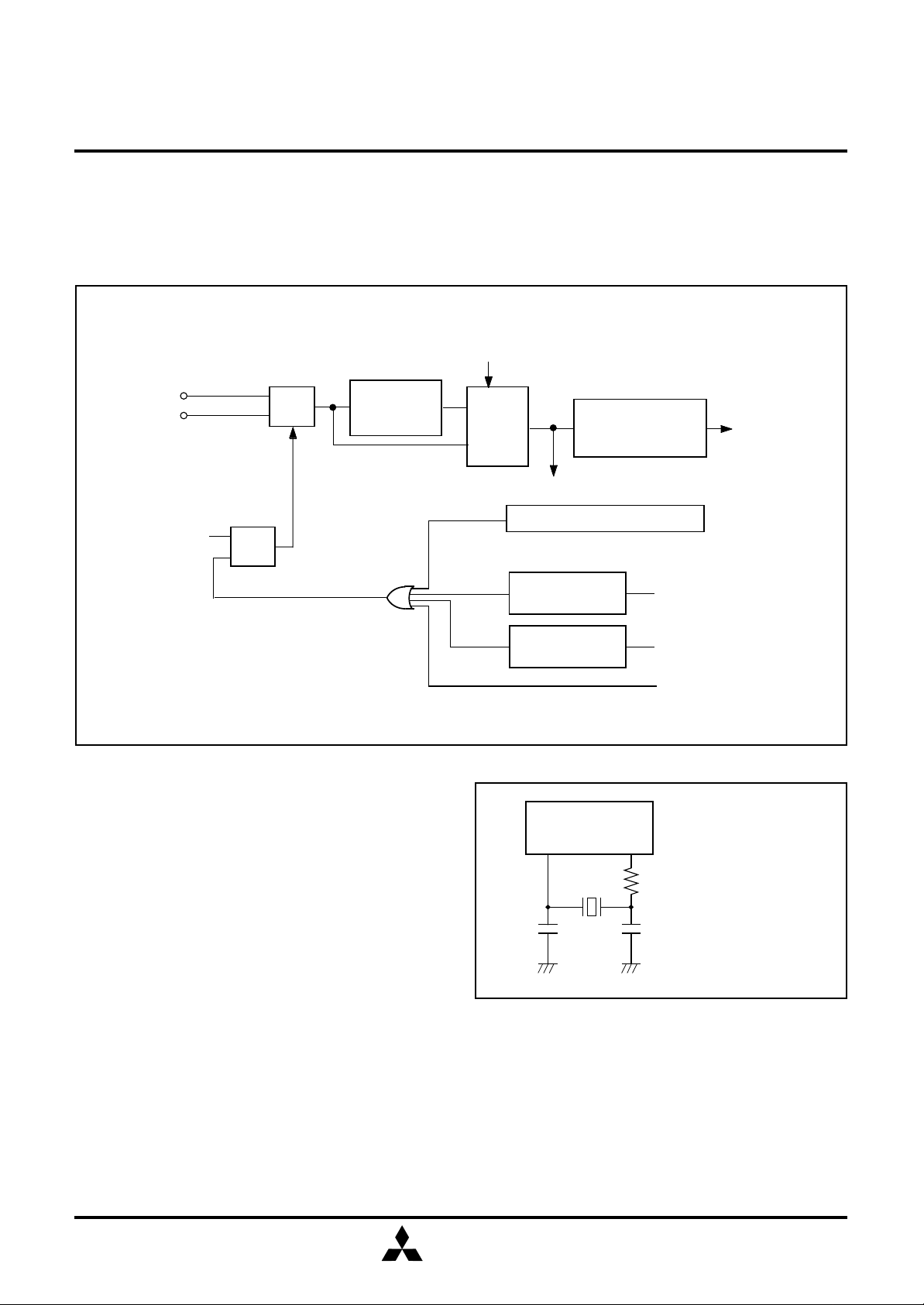
CLOCK CONTROL
The clock control circuit consists of the following circuits.
• System clock generating circuit
• Control circuit to stop the clock oscillation
• Control circuit to return from the RAM back-up state
MITSUBISHI MICROCOMPUTERS
4282 Group
SINGLE-CHIP 4-BIT CMOS MICROCOMPUTER
C C K i n s t r u c t i o n
X
I N
X
OUT
POF instruction
Fig. 25 Clock control circuit structure
System clock signal f(X
ceramic resonator. Connect this external circuit to pins X
X
OUT at the shortest distance as shown Figure 26.
A feedback resistor is built-in between X
IN) is obtained by externally connecting a
O S C
R
Q
S
F r e q u e n c y
d i v i d e r
( d i v i d e d b y 8 )
IN and
IN pin and XOUT pin.
ROM ORDERING METHOD
Please submit the information described below when ordering
Mask ROM.
(1) Mask ROM Order Confirmation Form
(2) Mark Specification Form
(3) Data to be written to ROM, in EPROM form (three identical
copies) or one floppy disk.
*
M u l t i p l e x e r
I n t e r n a l c l o c k
g e n e r a t i o n c i r c u i t
( d i v i d e d b y 4 )
STCK
I n t e r n a l p o w e r - o n r e s e t c i r c u i t
P u l l - d o w n c o n t r o l
r e g i s t e r P U 0
Pull-down control
register 1
4282
X
IN
45
C
IN
X
P o r t s E0, E1, G0– G
Ports D4–D
P o r t E
OUT
C
OUT
INSTCK
3
7
2
Use the resonator
manufacturer’s
recommended value
because constants
such as capacitance
depend on the
resonator.
* For the mask ROM confirmation, refer to the “Mitsubishi MCU
Technical Information” Homepage (http://
www.infomicom.maec.co.jp/indexe.htm).
MITSUBISHI
ELECTRIC
Fig. 26 Ceramic resonator external circuit
21
Loading...