


 Loading...
MITSUBISHI MICROCOMPUTERS
M37271MF-XXXSP M37271EF-XXXSP, M37271EFSP
SINGLE-CHIP 8-BIT CMOS MICROCOMPUTER with CLOSED CAPTION DECODER and ON-SCREEN DISPLAY CONTROLLER
DESCRIPTION
The M37271MF-XXXSP is a single-chip microcomputer designed with
CMOS silicon gate technology. It is housed in a 52-pin shrink plastic molded DIP.
In addition to their simple instruction sets, the ROM, RAM and I/O addresses are placed on the same memory map to enable easy programming.
The M37271MF-XXXSP has a OSD function and a data slicer function, so it is useful for a channel selection system for TV with a closed caption decoder. The features of the M37271EF-XXXSP and the
M37271EFSP are similar to those of the M37271MF-XXXSP except that these chips have a built-in PROM which can be written electrically.
FEATURES |
|
|
• Number of basic instructions ..................................................... |
|
71 |
• Memory size |
|
|
ROM ........................................................ |
|
60 K bytes |
RAM ........................................................ |
|
1024 bytes |
ROM for OSD ....................................... |
|
14464 bytes |
RAM for OSD ......................................... |
|
1920 bytes |
• The minimum instruction execution time |
|
|
.......................................... 0.5µs (at 8 MHz oscillation frequency) |
||
• Power source voltage .................................................. |
|
5 V ± 10 % |
• Subroutine nesting ............................................. |
128 levels (Max.) |
|
• Interrupts ....................................................... |
18 types, 16 vectors |
|
• 8-bit timers .................................................................................. |
|
6 |
• Programmable I/O ports (Ports P0, P1, P2, P30, P31) |
.............. 26 |
|
• Input ports (Ports P40–P46, P63, P64) ......................................... |
|
9 |
• Output ports (Ports P52–P55) ...................................................... |
|
4 |
• 12 V withstand ports .................................................................. |
|
11 |
• LED drive ports ........................................................................... |
|
2 |
• Serial I/O ............................................................ |
8-bit 1 channel |
|
• Multi-master I2C-BUS interface ............................... |
1 (2 systems) |
|
• A-D converter (8-bit resolution) ................................... |
|
4 channels |
• PWM output circuit ........................................................... |
|
8-bit 7 |
• Interrupt interval determination circuit ......................................... |
|
1 |
• Power dissipation |
|
|
In high-speed mode .......................................................... |
|
165mW |
(at VCC = 5.5V, 8MHz oscillation frequency, CRT on, and Data |
||
slicer on) |
|
|
In low-speed mode .......................................................... |
|
0.33mW |
(at VCC = 5.5V, 32kHz oscillation frequency) |
|
|
• Data slicer |
|
|
• OSD function |
|
|
Display characters ............................... |
40 characters 16 lines |
|
Kinds of characters ..................................................... |
|
320 kinds |
(In EXOSD mode, they can be combined with 32 kinds of extra |
||
|
|
fonts) |
Dot structure ........................................ |
CC mode : 16 |
26 dots |
|
OSD mode : 16 |
20 dots |
|
EXOSD mode : 16 |
26 dots |
Kinds of character sizes ................................ |
CC mode : 2 types |
|
|
OSD mode : 14 types |
|
|
EXOSD mode : 6 types |
|
It can be specified by a character unit (maximum 7 kinds).
Character font coloring, character background coloring
It can be specified by a screen unit (maximum 7 kinds).
Extra font coloring, raster coloring, border coloring
Kinds of character colors |
............... CC mode : 7 kinds (R, G, B) |
|
OSD mode : 15 kinds (R, G, B, I) |
EXOSD mode : 7 kinds (R, G, B, I1, I2) |
|
Display position |
|
Horizontal ................................................................ |
256 levels |
Vertical .................................................................. |
1024 levels |
Attribute ...................... |
CC mode : smooth italic, underline, flash |
|
OSD mode : border |
|
EXOSD mode : border, |
|
extra font (32 kinds) |
Automatic solid space function
Window function
Dual layer OSD function
APPLICATION
TV with a closed caption decoder

MITSUBISHI MICROCOMPUTERS
M37271MF-XXXSP
M37271EF-XXXSP, M37271EFSP
SINGLE-CHIP 8-BIT CMOS MICROCOMPUTER with CLOSED CAPTION DECODER and ON-SCREEN DISPLAY CONTROLLER
PIN CONFIGURATION (TOP VIEW)
HSYNC |
|
|
|
|
|
|
|
|
|
|
|
|
1 |
|
|
52 |
|
|
|
|
|
|||||
VSYNC |
|
|
|
|
|
|
|
|
2 |
|
|
51 |
|||||
|
|
|
|
|||||
P40/AD4 |
|
|
|
|
|
|
|
|
3 |
|
|
50 |
|||||
|
|
|
|
|||||
P41/INT2 |
|
|
|
|
|
|
|
|
|
|
|
|
4 |
|
|
49 |
|
|
|
|
|
|||||
P42/TIM2 |
|
|
|
|
|
|
|
|
|
|
|
|
5 |
|
|
48 |
|
|
|
|
|
|||||
P43/TIM3 |
|
|
|
|
|
|
|
|
|
|
|
|
6 |
XXXSP,-M37271EF |
XXXSP-M37271MF |
47 |
|
|
|
|||||||
|
|
|
|
|
|
|
||
P24/AD3 |
|
|
|
7 |
46 |
|||
|
|
|
|
|
||||
P25/AD2 |
|
|
|
|
|
|
|
|
|
|
|
8 |
|
|
45 |
||
|
|
|
||||||
P26/AD1 |
|
|
|
|
|
|
|
|
|
|
|
9 |
|
|
44 |
||
|
|
|
||||||
|
|
|
|
|
|
|
|
|
P27 |
|
|
|
10 |
|
|
43 |
|
|
|
|
||||||
P00/PWM4 |
|
|
|
|
|
|
|
|
11 |
|
|
42 |
|||||
|
|
|
||||||
P01/PWM5 |
|
|
|
|
|
|
|
|
|
12 |
|
|
41 |
||||
P02/PWM6 |
|
|
|
|
|
|
|
|
|
|
|
13 |
|
|
40 |
||
|
|
|
||||||
P17/SIN |
|
|
|
|
M37271EFSP |
|
|
|
14 |
|
39 |
||||||
|
|
|||||||
P44/INT1 |
|
|
|
|
|
|
|
|
|
|
|
|
15 |
|
38 |
||
|
|
|
|
|
||||
P45/SOUT |
|
|
|
|
|
|
|
|
16 |
|
|
37 |
|||||
|
|
|
||||||
P46/SCLK |
|
|
|
|
|
|
|
|
17 |
|
|
36 |
|||||
|
|
|
||||||
AVCC |
|
|
|
|
|
|
|
|
18 |
|
|
35 |
|||||
|
|
|
||||||
HLF |
|
|
|
|
|
|
|
|
19 |
|
|
34 |
|||||
|
|
|
||||||
RVCO |
|
|
|
|
|
|
|
|
|
20 |
|
|
33 |
||||
VHOLD |
|
|
|
|
|
|
|
|
|
|
21 |
|
|
32 |
|||
|
|
|
||||||
|
|
|
|
|
|
|||
CVIN |
|
|
22 |
|
|
31 |
||
|
|
|
||||||
|
|
|
|
|
|
|||
CNVSS |
|
|
|
23 |
|
|
30 |
|
|
|
|
||||||
XIN |
|
|
|
|
|
|
|
|
24 |
|
|
29 |
|||||
|
|
|
||||||
XOUT |
|
|
|
|
|
|
|
|
|
|
25 |
|
|
28 |
|||
|
|
|
||||||
|
|
|
|
|
|
|||
VSS |
|
|
26 |
|
|
27 |
||
|
|
|
|
|
|
|
|
|
P52/R
P53/G
P54/B
P55/OUT1
P04/PWM0
P05/PWM1
P06/PWM2
P07/PWM3
P20
P21
P22
P23
P10/OUT2
P11/SCL1
P12/SCL2
P13/SDA1
P14/SDA2
P15/I1
P16/I2/INT3
P03
P30
P31
RESET
P64/OSC2/XCOUT
P63/OSC1/XCIN
VCC
Outline 52P4B
2

FUNCTIONAL BLOCK DIAGRAM of M37271MF-XXXSP
Clock input Clock output
XIN XOUT
24 25
Clock generating
Address bus
|
|
|
Multi-master |
|
|
|
I2C-BUS interface |
||
P3 (2) |
SDA2 |
SDA1 |
SCL2 SCL1 |
P1 (8) |
|
|
|||
OUT2 INT3
Reset input
RESET AVCC VCC
30 |
18 |
27 |
A-D converter
P2 (8)
VSS CNVSS
26 23
SI/O (8)
|
|
|
SIN |
SCLK |
OUTS |
P0 (8) |
|
|
|||
|
|
|
|
|
|
|
|
|
|
|
|
|
|
|
|
|
|
|
|
|
|
|
|
|
|
|
|
|
|
32 31 |
14 34 35 36 37 38 39 40 |
10 |
9 |
8 |
7 |
41 42 43 44 |
45 46 47 48 33 13 12 11 |
I/O ports |
I/O port P1 |
|
|
I/O port P2 |
I/O port P0 |
||
P30, P31 |
|
|
|
|
|
|
|
3
Pins for data slicer
|
VHOLD |
HLF |
|
CVIN |
RVCO |
|
|
22 |
21 |
20 |
19 |
Data slicer
Input ports P63, P64
Clock input for OSD/ |
Clock output for OSD/ |
sub-clock input |
sub-clock output |
OSC1 |
OSC2 |
28 |
29 |
|
|
|
|
INT1 |
INT2 |
8-bit |
|
|
|
|
|
|
|
|
PWM circuit |
|
|
|
|
||
|
|
|
|
|
|
|
|
|
|
|
P4 (7) |
|
|
|
|
PWM6 PWM5 PWM4 PWM3 PWM2 PWM1 PWM0 |
P6 (2) |
P5 (4) |
|
|
|
|
|
|
|
|
|
OUT1 |
B G R |
VSYNC |
HSYNC |
|
17 16 15 |
6 |
5 |
4 |
3 |
|
|
49 50 51 52 |
2 |
1 |
|
Input ports P40–P46 |
|
|
Output port P5 |
Sync |
||||||
signal input
DECODER CAPTION CLOSED with MICROCOMPUTER CMOS BIT-8 CHIP-SINGLE CONTROLLER DISPLAY SCREEN-ON and
XXXSP-M37271MF M37271EFSP XXXSP,-M37271EF |
MICROCOMPUTERS MITSUBISHI |

MITSUBISHI MICROCOMPUTERS
M37271MF-XXXSP
M37271EF-XXXSP, M37271EFSP
SINGLE-CHIP 8-BIT CMOS MICROCOMPUTER with CLOSED CAPTION DECODER and ON-SCREEN DISPLAY CONTROLLER
FUNCTIONS
Parameter |
|
|
|
|
Functions |
|
Number of basic instructions |
|
|
71 |
|
|
|
|
|
|
|
|||
Instruction execution time |
|
|
0.5 μs (the minimum instruction execution time, at 8 MHz oscillation fre- |
|||
|
|
|
quency) |
|||
|
|
|
|
|||
Clock frequency |
|
|
8 MHz (maximum) |
|||
|
|
|
|
|||
Memory size |
ROM |
|
60 K bytes |
|||
|
|
|
|
|||
|
RAM |
|
1024 bytes |
|||
|
|
|
|
|||
|
OSD ROM |
|
14464 bytes |
|||
|
|
|
|
|||
|
OSD RAM |
|
1920 bytes |
|||
|
|
|
|
|||
Input/Output ports |
P00–P02, |
I/O |
7-bit 1 (N-channel open-drain output structure, can be used as PWM |
|||
|
P04–P07 |
|
output pins) |
|||
|
|
|
|
|||
|
P03 |
I/O |
1-bit 1 (CMOS input/output structure) |
|||
|
|
|
|
|||
|
P10, P15–P17 |
I/O |
4-bit 1 (CMOS input/output structure, can be used as OSD output pin, |
|||
|
|
|
INT input pin, serial input pin) |
|||
|
|
|
|
|||
|
P11–P14 |
I/O |
4-bit 1 (N-channel open-drain output structure, can be used as multi- |
|||
|
|
|
master I2C-BUS interface) |
|||
|
P2 |
I/O |
8-bit 1 (CMOS input/output structure, can be used as A-D input pins) |
|||
|
|
|
|
|||
|
P30, P31 |
I/O |
2-bit 1 (CMOS input/output structure) |
|||
|
P40–P44 |
Input |
5-bit 1 (can be used as A-D input pins, INT input pins, external clock |
|||
|
|
|
input pins) |
|||
|
P45, P46 |
Input |
2-bit 1 (N-channel open-drain output structure when serial I/O is used, |
|||
|
|
|
can be used as serial I/O pins) |
|||
|
P52–P55 |
Output |
4-bit 1 (CMOS output structure, can be used as OSD output) |
|||
|
P63 |
Input |
1-bit 1 (can be used as sub-clock input pin, OSD clock input pin) |
|||
|
P64 |
Input |
1-bit 1 (CMOS output structure when LC is oscillating, can be used as |
|||
|
|
|
sub-clock output pin, OSD clock output pin) |
|||
|
|
|
|
|||
Serial I/O |
|
|
8-bit 1 |
|||
|
|
|
|
|
|
|
Multi-master I2C-BUS interface |
|
|
1 |
|
|
|
A-D converter |
|
|
4 channels (8-bit resolution) |
|||
|
|
|
|
|||
PWM output circuit |
|
|
8-bit 7 |
|||
|
|
|
|
|||
Timers |
|
|
8-bit timer 6 |
|||
|
|
|
|
|||
Subroutine nesting |
|
|
128 levels (maximum) |
|||
|
|
|
|
|
|
|
Interrupt interval determination circuit |
|
1 |
|
|
|
|
|
|
|
|
|||
Interrupt |
|
|
External interrupt 3, Internal timer interrupt 6, Serial I/O interrupt 1, |
|||
|
|
|
OSD interrupt 1, Multi-master I2C-BUS interface interrupt 1, |
|||
|
|
|
Data slicer interrupt 1, f(XIN)/4092 interrupt 1, VSYNC interrupt 1, A- |
|||
|
|
|
D conversion interrupt 1, BRK instruction interrupt 1 |
|||
|
|
|
|
|||
Clock generating circuit |
|
|
2 built-in circuits (externally connected a ceramic resonator or a quartz- |
|||
|
|
|
crystal oscillator) |
|||
|
|
|
|
|||
Data slicer |
|
|
Built in |
|||
|
|
|
|
|
|
|
|
|
|
|
|
|
|
|
|
|
|
|
|
|
4

MITSUBISHI MICROCOMPUTERS
M37271MF-XXXSP
M37271EF-XXXSP, M37271EFSP
SINGLE-CHIP 8-BIT CMOS MICROCOMPUTER with CLOSED CAPTION DECODER and ON-SCREEN DISPLAY CONTROLLER
FUNCTIONS (continued)
OSD function |
|
Number of display characters |
40 characters 16 lines |
|||||
|
|
|
|
|
|
|||
|
|
Dot structure |
|
CC mode: 16 26 dots (character part : 16 20 dots) |
||||
|
|
|
|
|
OSD mode: 16 20 dots |
|||
|
|
|
|
|
EXOSD mode: 16 26 dots |
|||
|
|
Kinds of characters |
320 kinds |
|||||
|
|
|
|
|
(In EXOSDmode, they can be combined with 32 kinds of extra fonts) |
|||
|
|
Kinds of character sizes |
CC mode: 2 kinds |
|||||
|
|
|
|
|
OSD mode: 14 kinds |
|||
|
|
|
|
|
EXOSD mode: 6 kinds |
|||
|
|
|
|
|
|
|||
|
|
Kinds of character colors |
CC mode: 7 kinds (R, G, B) |
|||||
|
|
|
|
|
OSD mode: 15 kinds (R, G, B, I1) |
|||
|
|
|
|
|
EXOSD mode: 7 kinds (R, G, B, I1, I2) |
|||
|
|
|
|
|
|
|||
|
|
Display position (horizontal, vertical) |
256 levels (horizontal) 1024 levels (vertical) |
|||||
|
|
|
|
|
|
|||
Power source voltage |
|
|
5 V ± 10 % |
|||||
|
|
|
|
|
||||
Power dissipation |
In high-speed |
OSD ON |
Data slicer ON |
165 mW typ. (at oscillation frequency fCPU = 8 MHz, fOSD = 13 MHz) |
||||
|
mode |
OSD OFF |
Data slicer OFF |
82.5 mW typ. (at oscillation frequency fCPU = 8 MHz) |
||||
|
|
|
||||||
|
In low-speed |
OSD OFF |
Data slicer OFF |
0.33mW typ. (at oscillation frequency fCLK = 32 kHz, f(XIN) = stopped) |
||||
|
mode |
|
|
|
|
|
|
|
|
|
|
|
|
||||
|
In stop mode |
|
|
0.055 mW (maximum) |
||||
Operating temperature range |
|
|
–10 °C to 70 °C |
|||||
|
|
|
|
|
|
|||
Device structure |
|
|
|
|
CMOS silicon gate process |
|||
Package |
|
|
|
|
52-pin shrink plastic molded DIP |
|||
|
|
|
|
|
|
|
|
|
|
|
|
|
|
|
|
|
|
|
|
|
|
|
|
|
|
|
|
|
|
|
|
|
|
|
|
5

MITSUBISHI MICROCOMPUTERS
M37271MF-XXXSP
M37271EF-XXXSP, M37271EFSP
SINGLE-CHIP 8-BIT CMOS MICROCOMPUTER with CLOSED CAPTION DECODER and ON-SCREEN DISPLAY CONTROLLER
PIN DESCRIPTION
Pin |
Name |
Input/ |
|
|
|
|
|
Name |
||
Output |
|
|
|
|
|
|||||
|
|
|
|
|
|
|
|
|
||
|
|
|
|
|
||||||
VCC, |
Power source |
|
Apply voltage of 5 V ± 10 % (typical) to VCC and AVCC, and 0 V to VSS. |
|||||||
AVCC, |
|
|
|
|
|
|
|
|
||
VSS. |
|
|
|
|
|
|
|
|
||
|
|
|
|
|
||||||
CNVSS |
CNVSS |
|
This is connected to VSS. |
|||||||
_____ |
|
Reset input |
Input |
To enter the reset state, the reset input pin must be kept at a “L” for 2 μs or more (under |
||||||
RESET |
||||||||||
|
|
|
|
normal VCC conditions). |
||||||
|
|
|
|
If more time is needed for the quartz-crystal oscillator to stabilize, this “L” condition should |
||||||
|
|
|
|
be maintained for the required time. |
||||||
|
|
|
|
|
||||||
XIN |
Clock input |
Input |
This chip has an internal clock generating circuit. To control generating frequency, an |
|||||||
|
|
|
|
external ceramic resonator or a quartz-crystal oscillator is connected between pins XIN and |
||||||
XOUT |
Clock output |
Output |
XOUT. If an external clock is used, the clock source should be connected to the XIN pin and |
|||||||
|
|
|
|
the XOUT pin should be left open. |
||||||
|
|
|
|
|
||||||
P00/PWM4– |
I/O port P0 |
I/O |
Port P0 is an 8-bit I/O port with direction register allowing each I/O bit to be individually |
|||||||
P02/PWM6, |
|
|
programmed as input or output. At reset, this port is set to input mode. The output structure |
|||||||
P03, |
|
|
of P03 is CMOS output, that of P00–P02 and P04–P07 are N-channel open-drain output. |
|||||||
P04/PWM0– |
|
|
The note out of this Table gives a full of port P0 function. |
|||||||
P07/PWM3 |
|
|
|
|
|
|
|
|
||
PWM output |
Output |
Pins P00–P02 and P04–P07 are also used as PWM output pins PWM4–PWM6 and PWM0– |
||||||||
|
|
|||||||||
|
|
|
|
PWM3 respectively. The output structure is N-channel open-drain output. |
||||||
|
|
|
|
|
||||||
P10/OUT2, |
I/O port P1 |
I/O |
Port P1 is an 8-bit I/O port and has basically the same functions as port P0. The output |
|||||||
P11/SCL1, |
|
|
structure of P10 and P15–P17 is CMOS output, that of P11–P14 is N-channel open-drain |
|||||||
P12/SCL2, |
|
|
output. |
|
|
|
|
|
||
P13/SDA1, |
|
|
|
|||||||
OSD output |
Output |
Pins P10, P15, P16 are also used as OSD output pins OUT2, I1, I2 respectively. The output |
||||||||
P14/SDA2, |
|
|
structure is CMOS output. |
|||||||
P15/I1, |
|
|
||||||||
|
|
|
|
|
|
|
|
|||
Multi-master |
Output |
Pins P11–P14 are used as SCL1, SCL2, SDA1 and SDA2 respectively, when multi-master |
||||||||
P16/I2/INT3, |
||||||||||
P17/SIN |
I2C-BUS interface |
|
I2C-BUS interface is used. The output structure is N-channel open-drain output. |
|||||||
|
|
Serial I/O data |
Input |
P17 pin is also used as serial I/O data input pin SIN. |
||||||
|
|
input |
|
|
|
|
|
|
|
|
P20–P23 |
I/O port P2 |
I/O |
Port P2 is an 8-bit I/O port and has basically the same functions as port P0. The output |
|||||||
P24/AD3– |
|
|
structure is CMOS output. |
|||||||
P26/AD1, |
|
|
|
|
|
|
|
|
||
Analog input |
Input |
Pins P24–P26 are also used as analog input pins AD3–AD1 respectively. |
||||||||
P27 |
||||||||||
|
|
|
|
|
|
|
|
|||
|
|
|
|
|
||||||
P30, P31 |
I/O port P3 |
I/O |
Ports P30 and P31 are a 2-bit I/O port and has basically the same functions as port P0. The |
|||||||
|
|
|
|
output structure is CMOS output. |
||||||
|
|
|
|
|
||||||
P40/AD4, |
Input port P4 |
Input |
Ports P40–P46 are a 7-bit input port. |
|||||||
P41/INT2, |
|
|
|
|
|
|
|
|
||
Analog input |
Input |
P40 pin is also used as analog input pin AD4. |
||||||||
P42/TIM2, |
||||||||||
|
|
|
|
|
|
|
|
|||
External interrupt |
Input |
Pins P4 |
|
|
|
|
|
|||
P43/TIM3, |
1 |
4 |
|
|
|
|||||
|
|
, P4 are also used as external interrupt input INT2, INT1. |
||||||||
P44/INT1, |
input |
|
|
|
|
|
|
|
||
P45/SOUT, |
|
|
|
|
|
|
|
|
||
External clock input |
Input |
Pins P42 and P43 are also used as external clock input pins TIM2, TIM3 respectively. |
||||||||
P46/SCLK, |
||||||||||
|
|
|
|
|
|
|
|
|||
Serial I/O data |
Output |
P45 pin is used as serial I/O data output pin SOUT. The output structure is N-channel open- |
||||||||
|
|
|||||||||
|
|
output |
|
drain output. |
||||||
|
|
|
|
|
||||||
|
|
Serial I/O |
I/O |
P46 pin is used as serial I/O synchronizing clock input/output pin SCLK. The output struc- |
||||||
|
|
synchronizing clock |
|
ture is N-channel open-drain output. |
||||||
|
|
input/output |
|
|
|
|
|
|
|
|
P52/R,P53/G, |
Output port P5 |
Output |
Ports P52–P55 are a 4-bit output port. The output structure is CMOS output. |
|||||||
P54/B, |
|
|
|
|
|
|
|
|
||
|
Output |
Pins P52–P55 are also used as OSD output pins R, G, B, OUT1 respectively. |
||||||||
P55/OUT1 |
OSD output |
|||||||||
|
|
|
|
|
|
|
|
|
|
|
|
|
|
|
|
|
|
|
|
|
|
|
|
|
|
|
|
|
|
|
|
|
|
|
|
|
|
|
|
|
|
|
|
6

MITSUBISHI MICROCOMPUTERS
M37271MF-XXXSP
M37271EF-XXXSP, M37271EFSP
SINGLE-CHIP 8-BIT CMOS MICROCOMPUTER with CLOSED CAPTION DECODER and ON-SCREEN DISPLAY CONTROLLER
PIN DESCRIPTION (continued)
P63/OSC1/ |
Input port |
Input |
Ports P63 and P64 are 2-bit input port. |
||
XCIN, |
|
|
|
||
Clock input for OSD |
Input |
P63 pin is also used as OSD clock input pin OSC1. |
|||
P64/OSC2/ |
|
||||
|
|
|
|
||
|
Clock output for OSD |
Output |
P64 pin is also used as OSD clock output pin OSC2. The output structure is CMOS output. |
||
XCOUT |
|||||
|
|
|
|
|
|
|
|
Sub-clock output |
Output |
P64 pin is also used as sub-clock output pin XCOUT. The output structure is CMOS output. |
|
|
|
|
|
|
|
|
|
Sub-clock input |
Input |
P63 pin is also used as sub-clock input pin XCIN. |
|
|
|
|
|
||
CVIN |
I/O for data slicer |
Input |
Input composite video signal through a capacitor. |
||
|
|
|
|
||
VHOLD |
|
Input |
Connect a capacitor between VHOLD and VSS. |
||
|
|
|
|
||
RVCO |
|
|
Connect a resistor between RVCO and VSS. |
||
|
|
|
|
||
HLF |
|
|
Connect a filter using of a capacitor and a resistor between HLF and VSS. |
||
|
|
|
|
||
HSYNC |
HSYNC input |
Input |
This is a horizontal synchronizing signal input for OSD. |
||
|
|
|
|
||
VSYNC |
VSYNC input |
Input |
This is a vertical synchronizing signal input for OSD. |
||
|
|
|
|
|
|
Note : As shown in the memory map (Figure 3), port P0 is accessed as a memory at address 00C016 of zero page. Port P0 has the port P0 direction register (address 00C116 of zero page) which can be used to program each bit as an input (“0”) or an output (“1”). The pins programmed as “1” in the direction register are output pins. When pins are programmed as “0,” they are input pins. When pins are programmed as output pins, the output data are written into the port latch and then output. When data is read from the output pins, the output pin level is not read but the data of the port latch is read. This allows a previously-output value to be read correctly even if the output “L” voltage has risen, for example, because a light emitting diode was directly driven. The input pins are in the floating state, so the values of the pins can be read. When data is written into the input pin, it is written only into the port latch, while the pin remains in the floating state.
7

MITSUBISHI MICROCOMPUTERS
M37271MF-XXXSP
M37271EF-XXXSP, M37271EFSP
SINGLE-CHIP 8-BIT CMOS MICROCOMPUTER with CLOSED CAPTION DECODER and ON-SCREEN DISPLAY CONTROLLER
FUNCTIONAL DESCRIPTION
Central Processing Unit (CPU)
The M37271MF-XXXSP uses the standard 740 family instruction set. Refer to the table of 740 family addressing modes and machine instructions or the SERIES 740 < Software > User’s Manual for details on the instruction set.
Machine-resident 740 family instructions are as follows:
The FST, SLW instruction cannot be used.
The MUL, DIV, WIT and STP instruction can be used.
CPU Mode Register
The CPU mode register contains the stack page selection bit and internal system clock selection bit. The CPU mode register is allocated at address 00FB16.
7 |
|
|
0 |
CPU mode register |
|||
1 |
1 |
0 |
0 |
||||
(CPUM (CM) : address 00FB16) |
|||||||
|
|
|
|
||||
|
|
|
|
Processor mode bits |
|||
|
|
|
|
b1 b0 |
|
||
|
|
|
|
0 |
0 |
: Single-chip mode |
|
|
|
|
|
0 |
1 |
: |
|
|
|
|
|
1 |
0 |
: Not available |
|
|
|
|
|
1 |
1 |
: |
|
 Stack page selection bit (Note) 0 : Zero page
1 : 1 page
 Fix these bits to “1.”
 XCOUT drivability selection bit 0 : Low drive
1 : High drive
Main colock (XIN–XOUT) stop bit 0 : Oscillating
1 : Stopped
 Internal system clock selection bit
0 : XIN–XOUT selected (high-speed mode) 1 : XCIN–XCOUT selected (low-speed mode)
Note: Please beware of this bit when programming because it is set to “1” after the reset release.
Fig. 1. Structure of CPU mode register
8

MITSUBISHI MICROCOMPUTERS
M37271MF-XXXSP
M37271EF-XXXSP, M37271EFSP
SINGLE-CHIP 8-BIT CMOS MICROCOMPUTER with CLOSED CAPTION DECODER and ON-SCREEN DISPLAY CONTROLLER
MEMORY
Special Function Register (SFR) Area
The special function register (SFR) area in the zero page contains control registers such as I/O ports and timers.
RAM
RAM is used for data storage and for stack area of subroutine calls and interrupts.
ROM
ROM is used for storing user programs as well as the interrupt vector area.
RAM for OSD
RAM for display is used for specifying the character codes and colors to display.
Interrupt Vector Area
The interrupt vector area contains reset and interrupt vectors.
Zero Page
The 256 bytes from addresses 000016 to 00FF16 are called the zero page area. The internal RAM and the special function registers (SFR) are allocated to this area.
The zero page addressing mode can be used to specify memory and register addresses in the zero page area. Access to this area with only 2 bytes is possible in the zero page addressing mode.
Special Page
The 256 bytes from addresses FF0016 to FFFF16 are called the special page area. The special page addressing mode can be used to specify memory addresses in the special page area. Access to this area with only 2 bytes is possible in the special page addressing mode.
ROM for OSD
ROM for display is used for storing character data.
|
000016 |
|
1000016 |
|
|
|
Not used |
||
|
|
|
|
|
|
|
|
1080016 |
|
|
00C016 |
|
Zero page |
|
|
SFR1 area |
|
|
|
|
00FF16 |
|
|
|
|
|
|
|
|
RAM |
|
|
|
|
(1024 bytes) |
020016 |
|
|
|
|
SFR2 area |
|
|
|
|
023F16 |
1567F16 |
||
|
|
|||
|
|
Not used |
|
Not used |
|
030016 |
|
|
|
|
|
1800016 |
|
|
|
|
|
|
|
|
053F16 |
|
ROM for OSD |
|
|
|
Not used |
(14464 bytes) |
|
|
|
|
|
|
RAM for OSD (Note) |
080016 |
|
|
|
0FFF16 |
|
|
|
|
(1920 bytes) |
|
|
|
|
100016 |
|
|
|
|
|
|
|
|
|
ROM (60 K bytes)
FF0016 |
|
|
1E43F16 |
FFDE16 |
Interrupt vector area |
Special page |
Not used |
|
|
||
FFFF16 |
|
1FFFF16 |
|
|
|
Fig. 2. Memory map
9

MITSUBISHI MICROCOMPUTERS
M37271MF-XXXSP
M37271EF-XXXSP, M37271EFSP
SINGLE-CHIP 8-BIT CMOS MICROCOMPUTER with CLOSED CAPTION DECODER and ON-SCREEN DISPLAY CONTROLLER
■SFR1 area (addresses C016 to DF16)
: Nothing is allocated
: Fix this bit to “0” ( do not write “1”)
0: “0” immediately after reset
?: undefined immediately after reset
Address |
Register |
|
C016 |
Port P0 (P0) |
|
C116 |
Port P0 direction register (D0) |
|
C216 |
Port P1 (P1) |
|
C316 |
Port P1 direction register (D1) |
|
C416 |
Port P2 (P2) |
|
C516 |
Port P2 direction register (D2) |
|
C616 |
Port P3 (P3) |
|
C716 |
Port P3 direction register (D3) |
|
C816 |
Port P4 (P4) |
|
C916 |
Port P4 direction register (D4) |
|
CA16 |
Port P5 (P5) |
|
CB16 |
OSD port control register (PF) |
|
CC16 |
Port P6 (P6) |
|
CD16 |
|
|
CE16 |
OSD control register (OC) |
|
CF16 |
Horizontal position register (HP) |
|
D016 |
Block control register 1 (BC1) |
|
D116 |
Block control register 2 (BC2) |
|
D216 |
Block control register 3 (BC3) |
|
D316 |
Block control register 4 (BC4) |
|
D416 |
Block control register 5 (BC5) |
|
D516 |
Block control register 6 (BC6) |
|
D616 |
Block control register 7 (BC7) |
|
D716 |
Block control register 8 (BC8) |
|
D816 |
Block control register 9 (BC9) |
|
D916 |
Block control register 10 (BC10) |
|
DA16 |
Block control register 11 (BC11) |
|
DB16 |
Block control register 12 (BC12) |
|
DC16 |
Block control register 13 (BC13) |
|
DD16 |
Block control register 14 (BC14) |
|
DE16 |
Block control register 15 (BC15) |
|
DF16 |
Block control register 16 (BC16) |
|
Bit allocation
b7 |
|
|
|
b0 |
|
|
|
|
|
|
|
|
|
|
|
|
|
|
|
|
|
|
|
|
OUT2 OUT1 |
B |
G |
R |
I2 |
I1 |
OC7 OC6 OC5 OC4 OC3 OC2 OC1 OC0 |
HP7 HP6 HP5 HP4 HP3 HP2 HP1 HP0 |
BC18 BC17 BC16 BC15 BC14 BC13 BC12 BC11 |
|
BC28 |
BC27 |
BC26 |
BC25 |
BC24 |
BC23 |
BC22 |
BC21 |
|
|
BC38 |
BC37 |
BC36 |
BC35 |
BC34 |
BC33 |
BC32 |
BC31 |
|
|
BC48 |
BC47 |
BC46 |
BC45 |
BC44 |
BC43 |
BC42 |
BC41 |
|
|
BC58 |
BC57 |
BC56 |
BC55 |
BC54 |
BC53 |
BC52 |
BC51 |
|
|
BC68 |
BC67 |
BC66 |
BC65 |
BC64 |
BC63 |
BC62 |
BC61 |
|
|
BC78 |
BC77 |
BC76 |
BC75 |
BC74 |
BC73 |
BC72 |
BC71 |
|
|
BC88 |
BC87 |
BC86 |
BC85 |
BC84 |
BC83 |
BC82 |
BC81 |
|
|
BC98 |
BC97 |
BC96 |
BC95 |
BC94 |
BC93 |
BC92 |
BC91 |
|
|
BC108 |
BC107 |
BC106 |
BC105 |
BC104 |
BC103 |
BC102 |
BC101 |
|
|
BC118 |
BC117 |
BC116 |
BC115 |
BC114 |
BC113 |
BC112 |
BC111 |
|
|
BC128 |
BC127 |
BC126 |
BC125 |
BC124 |
BC123 |
BC122 |
BC121 |
|
|
BC138 |
BC137 |
BC136 |
BC135 |
BC134 |
BC133 |
BC132 |
BC131 |
|
|
BC148 |
BC147 |
BC146 |
BC145 |
BC144 |
BC143 |
BC142 |
BC141 |
|
|
BC158 |
BC157 |
BC156 |
BC155 |
BC154 |
BC153 |
BC152 |
BC151 |
|
|
BC168 |
BC167 |
BC166 |
BC165 |
BC164 |
BC163 |
BC162 |
BC161 |
|
State immediately after reset
b7 |
|
|
|
|
|
|
|
b0 |
|
|
|
|
? |
|
|
|
|
|
|
|
0016 |
|
|
|
||
|
|
|
|
? |
|
|
|
|
|
|
|
0016 |
|
|
|
||
|
|
|
|
? |
|
|
|
|
|
|
|
0016 |
|
|
|
||
? |
? |
? |
? |
? |
? |
? |
? |
|
0 |
0 |
0 |
0 |
|
0 |
0 |
0 |
0 |
? |
? |
? |
? |
? |
? |
? |
? |
0 |
0 |
0 |
0 |
0 |
0 |
0 |
0 |
? |
? |
? |
? |
? |
? |
? |
? |
0 |
0 |
0 |
0 |
0 |
0 |
0 |
0 |
? |
? |
? |
? |
? |
? |
? |
? |
?
0016
0016
?
?
?
?
?
?
?
?
?
?
?
?
?
?
?
?
Fig. 3. Memory map of special function register 1 (SFR1) (1)
10
MITSUBISHI MICROCOMPUTERS
M37271MF-XXXSP
M37271EF-XXXSP, M37271EFSP
SINGLE-CHIP 8-BIT CMOS MICROCOMPUTER with CLOSED CAPTION DECODER and ON-SCREEN DISPLAY CONTROLLER
■SFR1 area (addresses E016 to FF16)
 : Nothing is allocated
: Fix this bit to |
“0” ( do |
not write “1”) |
: Fix this bit to |
“1” ( do |
not write “0”) |
0: “0” immediately after reset
1: “1” immediately after reset
?: undefined immediately after reset
Address |
Register |
|
E016 |
Caption position register (CP) |
|
E116 |
Start bit position register (SP) |
|
E216 |
Window register (WN) |
|
E316 |
Sync slice register (SSL) |
|
E416 |
Data register 1 (CD1) |
|
E516 |
Data register 2 (CD2) |
|
E616 |
Clock run-in register 1 (CR1) |
|
E716 |
Clock run-in register 2 (CR2) |
|
E816 |
Clock run-in detect register 1 (CRD1) |
|
E916 |
Clock run-in detect register 2 (CRD2) |
|
EA16 |
Data slicer control register 1 (DSC1) |
|
EB16 |
Data slicer control register 2 (DSC2) |
|
EC16 |
Data register 3 (CD3) |
|
ED16 |
Data register 4 (CD4) |
|
EE16 |
A-D conversion register (AD) |
|
EF16 |
A-D control register (ADCON) |
|
F016 |
Timer 1 (TM1) |
|
F116 |
Timer 2 (TM2) |
|
F216 |
Timer 3 (TM3) |
|
F316 |
Timer 4 (TM4) |
|
F416 |
Timer mode register 1 (TM1) |
|
F516 |
Timer mode register 2 (TM2) |
|
F616 |
I2C data shift register (S0) |
|
F716 |
I2C address register (S0D) |
|
F816 |
I2C status register (S1) |
|
F916 |
I2C control register (S1D) |
|
FA16 |
I2C clock control register (S2) |
|
FB16 |
CPU mode register (CPUM) |
|
FC16 |
Interrupt request register 1 (IREQ1) |
|
FD16 |
Interrupt request register 2 (IREQ2) |
|
FE16 |
Interrupt control register 1 (ICON1) |
|
FF16 |
Interrupt control register 2 (ICON2) |
|
b7 |
Bit allocation |
b0 |
|
|
CP4 CP3 CP2 CP1 CP0 |
SP7 SP6 SP5 SP4 SP3 SP2 SP1 SP0  WN5 WN4 WN3 WN2 WN1 WN0
SSL7
CR11
CR21
CRD17 CRD15 CRD15 CRD15 CRD15 CRD12 CRD11 CRD10
CRD27 CRD25 CRD25 CRD25 CRD25 CRD22 CRD21 CRD20
DSC17 |
DSC15 |
DSC12 DSC11 DSC10 |
|
|
|
DSC27 |
DSC25 |
DSC22 DSC21 DSC20 |
ADV ADVREF ADSTR ADIN1 ADIN0
TM17 |
TM16 |
TM15 |
TM14 |
TM13 |
TM12 |
TM11 |
TM10 |
|
|
|
|
|
|
|
|
TM27 |
TM26 |
TM25 |
TM24 |
TM23 |
TM22 |
TM21 |
TM20 |
|
|
|
|
|
|
|
|
|
|
|
|||||
SAD6 SAD5 SAD4 SAD3 SAD2 |
SAD1 |
SAD0 RBW |
|||||
|
|
|
|
|
|||
MST TRX |
BB |
PIN AL |
AAS |
AD0 LRB |
|||
|
|
|
|
||||
BSEL1 BSEL0 |
10 BIT |
ALS ES0 BC2 |
BC1 BC0 |
||||
|
|
SAD |
|
|
|
|
|
ACK ACK |
FAST |
CCR4 CCR3 CCR2 |
CCR1 CCR0 |
||||
|
BIT |
MODE |
|
|
|
|
|
CM7 CM6 CM5 |
|
|
CM2 CM1 CM0 |
||||
|
|
|
|
|
|
|
|
ADR VSCRCRTRTM4R TM3R TM2R TM1R
T56R IICR INT2RCK01MSR SIOR DSR INT1R
ADE VSCE CRTE TM4E TM3E TM2E TM1E
T56S T56E IICE INT2E1MSE SIOE DSE INT1E
State immediately after reset
b7 |
|
|
|
|
|
|
b0 |
1 |
0 |
0 |
? |
? |
? |
? |
? |
|
|
|
0016 |
|
|
|
|
0 |
0 |
0 |
0 |
0 |
0 |
0 |
0 |
0 |
0 |
0 |
0 |
0 |
1 |
0 |
1 |
|
|
|
? |
|
|
|
|
|
|
|
? |
|
|
|
|
0 |
1 |
0 |
1 |
0 |
0 |
0 |
0 |
1 |
0 |
0 |
1 |
1 |
1 |
0 |
1 |
0 |
0 |
0 |
0 |
0 |
0 |
0 |
0 |
0 |
0 |
0 |
0 |
1 |
0 |
0 |
1 |
|
|
|
? |
|
|
|
|
? |
0 |
0 |
0 |
0 |
0 |
0 |
0 |
|
|
|
0016 |
|
|
|
|
|
|
|
0016 |
|
|
|
|
|
|
|
? |
|
|
|
|
0 |
? |
0 |
0 |
0 |
? |
0 |
0 |
|
|
|
FF16 |
|
|
|
|
|
|
|
0716 |
|
|
|
|
|
|
|
FF16 |
|
|
|
|
|
|
|
0716 |
|
|
|
|
0 |
0 |
0 |
0 |
0 |
0 |
0 |
0 |
0 |
0 |
0 |
0 |
0 |
0 |
0 |
0 |
|
|
|
? |
|
|
|
|
|
|
|
0016 |
|
|
|
|
0 |
0 |
0 |
1 |
0 |
0 |
0 |
? |
|
|
|
0016 |
|
|
|
|
|
|
|
0016 |
|
|
|
|
0 |
0 |
1 |
1 |
1 |
1 |
0 |
0 |
0 |
0 |
0 |
0 |
0 |
0 |
0 |
0 |
0 |
0 |
0 |
CK0 |
0 |
0 |
0 |
0 |
0 |
0 |
0 |
0 |
0 |
0 |
0 |
0 |
0 |
0 |
0 |
0 |
0 |
0 |
0 |
0 |
Fig. 4. Memory map of special function register 1 (SFR2) (2)
11

MITSUBISHI MICROCOMPUTERS
M37271MF-XXXSP
M37271EF-XXXSP, M37271EFSP
SINGLE-CHIP 8-BIT CMOS MICROCOMPUTER with CLOSED CAPTION DECODER and ON-SCREEN DISPLAY CONTROLLER
■SFR2 area (addresses 20016 to 21F16)
: Nothing is allocated
: Fix this bit to “0” ( do not write “1”)
0: “0” immediately after reset
1: “1” immediately after reset
?: undefined immediately after reset
Address Register
20016
20116
20216
20316
20416
20516
20616
20716
20816 Clock run-in detect register (CRD3)
20916 Clock run-in register (CR3)
20A16 PWM mode register 1 (PN)
20B16 PWM mode register 2 (PW)
20C16 Timer 5 (TM5)
20D16 Timer 6 (TM6)
20E16
20F16
21016
21116
21216
21316
21416
21516
21616
21716
21816
21916
21A16
21B16 Border color register (FC)
21C16 Window H register 1 (WH1)
21D16 Window L register 1 (WH1)
21E16 Window H register 2 (WH2)
21F16 Window L register 2 (WH2)
Bit allocation |
|
|
State immediately after reset |
b7 |
b0 |
b7 |
b0 |
CRD35 CRD34 CRD33 CRD32 CRD31

 POL
POL  ENABLE
PW6 PW5 PW4 PW3 PW2 PW1 PW0
 SYC5 SYC4 SYC3 SYC2 SYC1 SYC0
DSC37 DSC36 DSC35DSC34 DSC33 DSC32 DSC31 DSC30
AD/INT3 |
INT3 |
RE5 RE4 RE3 RE2 RE1 RE0 |
SEL |
POL |
|
AD/INT3 |
INT3 |
SMRE5 SM4 SMRE3 SMRE2 SMRE1 SM0 |
SEL |
POL |
|
AD/INT3 |
INT3 |
RE5CS |
CS4 |
RE3CS |
RE2CS |
RE1CS |
CS0 |
SEL |
CS6 |
||||||
POL |
|
|
|
|
|
|
|
AD/INT3 |
INT3 |
|
|
|
|
|
|
PC7 PC6 RE5PC5 PC4 RE3PC3 RE2PC2 RE1PC1 PC0 |
|||||||
SEL |
POL |
|
|
|
|
|
|
AD/INT3 |
INT3 |
|
|
|
|
|
|
RC7 RC6 RCE5 RC4 RCE3 RCE2 RCE1 RC0 |
|||||||
SEL |
POL |
|
|
|
|
|
|
AD/INT3 |
INT3 |
RE5 |
|
RE3 |
RE2 |
RE1 |
|
SEL |
POL |
|
|
|
|
|
|
|
|
|
|
|
|
|
|
|
|
|
FC4 |
FC3 |
FC2 |
FC1 |
FC0 |
|
|
|
|
|
|
|
|
|
|
|
|
|
|
|
|
|
|
|
|
|
|
|
|
WH21 WH20


 WL21 WL20
?
?
?
?
?
?
? 0 0 0 0 0 0 0
?
0 0 0 0 0 0 0 0
?? ? ? ? ? ? ?
? ? ? ? 0 ? ? 0
0 ? ? ? ? ? ? ?
0716
FF16
?
? ? 0 0 0 0 0 0
0016
?
0016
0 0 0 0 0 0 0  0
0
?
?
0 ? ? ? ? ? ? ?
1 0 0 0 0 0 0 0
0016
? ? ? 0 0 0 0  0
0
?
? ? ? 0 0 0 0  0
0
?
?
?? ? ? ? ? ? ?
?? ? ? ? ? ? ?
Fig. 5. Memory map of special function register 2 (SFR2) (1)
12
MITSUBISHI MICROCOMPUTERS
M37271MF-XXXSP
M37271EF-XXXSP, M37271EFSP
SINGLE-CHIP 8-BIT CMOS MICROCOMPUTER with CLOSED CAPTION DECODER and ON-SCREEN DISPLAY CONTROLLER
■SFR2 area (addresses 22016 to 23F16)
: Nothing is allocated
? : undefined immediately after reset
Address |
Register |
|
22016 |
Vertical position register 11 (VP11) |
|
22116 |
Vertical position register 12 (VP12) |
|
22216 |
Vertical position register 13 (VP13) |
22316 |
Vertical position register 14 (VP14) |
22416 |
Vertical position register 15 (VP15) |
22516 |
Vertical position register 16 (VP16) |
22616 |
Vertical position register 17 (VP17) |
22716 Vertical position register 18 (VP18)
22816 |
Vertical position register 19 (VP19) |
22916 |
Vertical position register 110 (VP110) |
22A16 |
Vertical position register 111 (VP111) |
22B16 |
Vertical position register 112 (VP112) |
22C16 Vertical position register 113 (VP113)
22D16 |
Vertical position register 114 (VP114) |
22E16 |
Vertical position register 115 (VP115) |
22F16 |
Vertical position register 116 (VP116) |
23016 |
Vertical position register 21 (VP21) |
23116 |
Vertical position register 22 (VP22) |
23216 |
Vertical position register 23 (VP23) |
23316 |
Vertical position register 24 (VP24) |
23416 |
Vertical position register 25 (VP25) |
23516 |
Vertical position register 26 (VP26) |
23616 |
Vertical position register 27 (VP27) |
23716 |
Vertical position register 28 (VP28) |
23816 |
Vertical position register 29 (VP29) |
23916 |
Vertical position register 210 (VP210) |
23A16 |
Vertical position register 211 (VP211) |
23B16 |
Vertical position register 212 (VP212) |
23C16 Vertical position register 213 (VP213)
23D16 Vertical position register 214 (VP214)
23E16 Vertical position register 215 (VP215)
23F16 Vertical position register 216 (VP216)
b7 |
Bit allocation |
b7 |
State immediately after reset |
||||||
b0 |
|
|
|
|
|
|
b0 |
||
VP118 VP117 VP116 VP115 VP114VP113 VP112 VP111 |
|
|
|
|
? |
|
|
|
|
VP128 VP127 VP126 VP125 VP124VP123 VP122 VP121 |
|
|
|
|
? |
|
|
|
|
VP138 VP137 VP136 VP135 VP134VP133 VP132 VP131 |
|
|
|
|
? |
|
|
|
|
VP148 VP147 VP146 VP145 VP144VP143 VP142 VP141 |
|
|
|
|
? |
|
|
|
|
VP158 VP157 VP156 VP155 VP154VP153 VP152 VP151 |
|
|
|
|
? |
|
|
|
|
VP168 VP167 VP166 VP165 VP164VP163 VP162 VP161 |
|
|
|
|
? |
|
|
|
|
VP178 VP177 VP176 VP175 VP174VP173 VP172 VP171 |
|
|
|
|
? |
|
|
|
|
VP188 VP187 VP186 VP185 VP184VP183 VP182 VP181 |
|
|
|
|
? |
|
|
|
|
VP198 VP197 VP196 VP195 VP194VP193 VP192 VP191 |
|
|
|
|
? |
|
|
|
|
VP1108 VP1107VP1106 VP1105 VP1104VP1103 VP1102 VP1101 |
|
|
|
|
? |
|
|
|
|
VP1118 VP1117VP1116 VP1115 VP1114VP1113 VP1112 VP1111 |
|
|
|
|
? |
|
|
|
|
VP1128 VP1127VP1126 VP1125 VP1124VP1123 VP1122 VP1121 |
|
|
|
|
? |
|
|
|
|
VP1138 VP1137VP1136 VP1135 VP1134VP1133 VP1132 VP1131 |
|
|
|
|
? |
|
|
|
|
VP1148 VP1147VP1146 VP1145 VP1144VP1143 VP1142 VP1141 |
|
|
|
|
? |
|
|
|
|
VP1158 VP1157VP1156 VP1155 VP1154VP1153 VP1152 VP1151 |
|
|
|
|
? |
|
|
|
|
VP1168 VP1167VP1166 VP1165 VP1164VP1163 VP1162 VP1161 |
|
|
|
|
? |
|
|
|
|
|
VP212 VP211 |
? |
? |
? |
? |
? |
? |
? |
? |
|
VP222 VP221 |
? |
? |
? |
? |
? |
? |
? |
? |
|
VP232 VP231 |
? |
? |
? |
? |
? |
? |
? |
? |
|
VP242 VP241 |
? |
? |
? |
? |
? |
? |
? |
? |
|
VP252 VP251 |
? |
? |
? |
? |
? |
? |
? |
? |
|
VP262 VP261 |
? |
? |
? |
? |
? |
? |
? |
? |
|
VP272 VP271 |
? |
? |
? |
? |
? |
? |
? |
? |
|
VP282 VP281 |
? |
? |
? |
? |
? |
? |
? |
? |
|
VP292 VP291 |
? |
? |
? |
? |
? |
? |
? |
? |
|
VP2102 VP2101 |
? |
? |
? |
? |
? |
? |
? |
? |
|
VP2112 VP2111 |
? |
? |
? |
? |
? |
? |
? |
? |
|
VP2122 VP2121 |
? |
? |
? |
? |
? |
? |
? |
? |
|
VP2132 VP2131 |
? |
? |
? |
? |
? |
? |
? |
? |
|
VP2142 VP2141 |
? |
? |
? |
? |
? |
? |
? |
? |
|
VP2152 VP2151 |
? |
? |
? |
? |
? |
? |
? |
? |
|
VP2162 VP2161 |
? |
? |
? |
? |
? |
? |
? |
? |
Fig. 6. Memory map of special function register 2 (SFR2) (2)
13

MITSUBISHI MICROCOMPUTERS
M37271MF-XXXSP
M37271EF-XXXSP, M37271EFSP
SINGLE-CHIP 8-BIT CMOS MICROCOMPUTER with CLOSED CAPTION DECODER and ON-SCREEN DISPLAY CONTROLLER

 : Nothing is allocated
1 : “1” immediately after reset
? : undefined immediately after reset
Register |
|
|
Bit allocation |
|
|
|
State immediately after reset |
||||||||||||||||
|
b7 |
b0 |
b7 |
|
|
|
|
|
|
|
b0 |
||||||||||||
Processor status register (PS) |
|
|
|
|
|
|
|
|
|
|
|
|
|
|
|
|
|
|
|
|
|
|
|
N |
V |
T |
B |
D |
I |
Z |
C |
|
? |
? |
? |
? |
? |
1 |
? |
? |
|
||||||
Program counter (PCH) |
|
|
|||||||||||||||||||||
|
|
|
|
|
|
|
|
|
|
|
|
|
|
Contents of address FFFF16 |
|
||||||||
Program counter (PCL) |
|
|
|
|
|
|
|
|
|
|
|
|
|
|
|
||||||||
|
|
|
|
|
|
|
|
|
|
|
|
|
|
Contents of address FFFE16 |
|
||||||||
|
|
|
|
|
|
|
|
|
|
|
|
|
|
|
|
||||||||
|
|
|
|
|
|
|
|
|
|
|
|
|
|
|
|
|
|
|
|
|
|
|
|
Fig. 7. Internal state of processor status register and program counter at reset |
|
|
|
|
|
|
|
|
|
|
|
|
|||||||||||
|
|
|
|
|
|
|
|
|
|
|
|
|
|
|
|
|
|
|
|
|
|
|
|
|
|
|
|
|
|
|
|
|
|
|
|
|
|
|
|
|
|
|
|
|
|
|
|
|
|
|
|
|
|
|
|
|
|
|
|
|
|
|
|
|
|
|
|
|
|
|
|
14

MITSUBISHI MICROCOMPUTERS
M37271MF-XXXSP
M37271EF-XXXSP, M37271EFSP
SINGLE-CHIP 8-BIT CMOS MICROCOMPUTER with CLOSED CAPTION DECODER and ON-SCREEN DISPLAY CONTROLLER
INTERRUPTS
Interrupts can be caused by 18 different sources consisting of 4 external, 12 internal, 1 software, and reset. Interrupts are vectored interrupts with priorities shown in Table 1. Reset is also included in the table because its operation is similar to an interrupt.
When an interrupt is accepted,
(1)The contents of the program counter and processor status register are automatically stored into the stack.
(2)The interrupt disable flag I is set to “1” and the corresponding interrupt request bit is set to “0.”
(3)The jump destination address stored in the vector address enters
the program counter.
Other interrupts are disabled when the interrupt disable flag is set to
“1.”
All interrupts except the BRK instruction interrupt have an interrupt request bit and an interrupt enable bit. The interrupt request bits are in interrupt request registers 1 and 2 and the interrupt enable bits are in interrupt control registers 1 and 2. Figure 8 shows the structure of the interrupt-related registers.
Interrupts other than the BRK instruction interrupt and reset are accepted when the interrupt enable bit is “1,” interrupt request bit is “1,” and the interrupt disable flag is “0.” The interrupt request bit can be set to “0” by a program, but not set to “1.” The interrupt enable bit can be set to “0” and “1” by a program.
Reset is treated as a non-maskable interrupt with the highest priority. Figure 9 shows interrupt control.
Interrupt Causes
(1)VSYNC and OSD interrupts
The VSYNC interrupt is an interrupt request synchronized with the vertical sync signal.
The OSD interrupt occurs after character block display to the CRT is completed.
(2)INT1, INT2, INT3 interrupts
With an external interrupt input, the system detects that the level of a pin changes from “L” to “H” or from “H” to “L,” and generates an interrupt request. The input active edge can be selected by bits 3, 4 and 6 of the interrupt interval determination control register (address 021216) : when this bit is “0,” a change from “L” to “H” is detected; when it is “1,” a change from “H” to “L” is detected. Note that all bits are cleared to “0” at reset.
(3)Timer 1, 2, 3 and 4 interrupts
An interrupt is generated by an overflow of timer 1, 2, 3 or 4.
(4)Serial I/O interrupt
This is an interrupt request from the clock synchronous serial I/O function.
(5)f(XIN)/4096 interrupt
This interrupt occurs regularly with a f(XIN)/4096 period. Set bit 0 of the PWM mode register 1 to “0.”
(6)Data slicer interrupt
An interrupt occurs when slicing data is completed.
(7)Multi-master I2C-BUS interface interrupt
This is an interrupt request related to the multi-master I2C-BUS interface.
(8)A-D conversion interrupt
An interrupt occurs at the completion of A-D conversion. Since A-D conversion interrupt and the INT3 interrupt share the same vector, an interrupt source is selected by bit 7 of the interrupt interval determination control register (address 021216).
Table 1. Interrupt vector addresses and priority
Interrupt source |
Priority |
Vector addresses |
Remarks |
|||
|
|
|
|
|||
Reset |
1 |
FFFF16, FFFE16 |
Non-maskable |
|||
|
|
|
|
|||
OSD interrupt |
2 |
FFFD16, FFFC16 |
|
|||
|
|
|
|
|||
INT1 interrupt |
3 |
FFFB16, FFFA16 |
Active edge selectable |
|||
|
|
|
|
|||
Data slicer interrupt |
4 |
FFF916, FFF816 |
|
|||
|
|
|
|
|||
Serial I/O interrupt |
5 |
FFF716, FFF616 |
|
|||
|
|
|
|
|||
Timer 4 interrupt |
6 |
FFF516, FFF416 |
|
|||
|
|
|
|
|||
f(XIN)/4096 interrupt |
7 |
FFF316, FFF216 |
|
|||
|
|
|
|
|||
VSYNC interrupt |
8 |
FFF116, FFF016 |
Active edge selectable |
|||
|
|
|
|
|||
Timer 3 interrupt |
9 |
FFEF16, FFEE16 |
|
|||
|
|
|
|
|||
Timer 2 interrupt |
10 |
FFED16, FFEC16 |
|
|||
|
|
|
|
|||
Timer 1 interrupt |
11 |
FFEB16, FFEA16 |
|
|||
|
|
|
|
|||
A-D convertion · INT3 interrupt |
12 |
FFE916, FFE816 |
Active edge selectable |
|||
|
|
|
|
|||
INT2 interrupt |
13 |
FFE716, FFE616 |
Active edge selectable |
|||
|
|
|
|
|||
Multi-master I2C-BUS interface interrupt |
14 |
FFE516, FFE416 |
|
|||
Timer 5 · 6 interrupt |
15 |
FFE316, FFE216 |
|
|||
|
|
|
|
|||
BRK instruction interrupt |
16 |
FFDF16, FFDE16 |
Non-maskable (software interrupt) |
|||
|
|
|
|
|
|
|
|
|
|
|
|
|
|
|
|
|
|
|
|
|
|
|
|
|
|
|
|
15
MITSUBISHI MICROCOMPUTERS
M37271MF-XXXSP
M37271EF-XXXSP, M37271EFSP
SINGLE-CHIP 8-BIT CMOS MICROCOMPUTER with CLOSED CAPTION DECODER and ON-SCREEN DISPLAY CONTROLLER
(9)Timer 5 · 6 interrupt
An interrupt is generated by an overflow of timer 5 or 6. Their priorities are same, and can be switched by software.
(10)BRK instruction interrupt
This software interrupt has the least significant priority. It does not have a corresponding interrupt enable bit, and it is not affected by the interrupt disable flag I (non-maskable).
Interrupt request bit
Interrupt enable bit
Interrupt disable flag I
BRK instruction
 Interrupt request
Reset
Fig. 9. Interrupt control
7 |
|
0 |
|
|
|
|
7 |
|
|
|
|
|
|
|
|
|
|
|
0 |
|
|
|
|||||||||||||||
|
|
|
|
|
|
|
|
|
|
|
|
|
|
|
Interrupt request register 1 |
0 |
|
|
|
|
|
|
|
|
|
|
|
|
|
|
Interrupt request register 2 |
||||||
|
|
|
|
|
|
|
|
|
|
|
|
|
|
|
(IREQ1: address 00FC |
16) |
|
|
|
|
|
|
|
|
|
|
|
|
|
|
(IREQ2: address 00FD 16) |
||||||
|
|
|
|
|
|
|
|
|
|
|
|
|
|
|
|
|
|
|
|
|
|
|
|
|
|
|
|
|
|
|
|||||||
|
|
|
|
|
|
|
|
|
|
|
|
|
|
|
|
|
Timer 1 interrupt request bit |
|
|
|
|
|
|
|
|
|
|
|
|
|
|
|
|
|
|
INT1 interrupt request bit |
|
|
|
|
|
|
|
|
|
|
|
|
|
|
|
|
|
|
|
|
|
|
|
|
|
|
|
|
|
|
|
|
|
|
|
||||
|
|
|
|
|
|
|
|
|
|
|
|
|
|
|
|
|
Timer 2 interrupt request bit |
|
|
|
|
|
|
|
|
|
|
|
|
|
|
|
|
|
|
Data slicer interrupt request bit |
|
|
|
|
|
|
|
|
|
|
|
|
|
|
|
|
|
|
|
|
|
|
|
|
|
|
|
|
|
|
|
|
|
|
|
|
|||
|
|
|
|
|
|
|
|
|
|
|
|
|
|
|
|
|
Timer 3 interrupt request bit |
|
|
|
|
|
|
|
|
|
|
|
|
|
|
|
|
|
|
Serial I/O interrupt request bit |
|
|
|
|
|
|
|
|
|
|
|
|
|
|
|
|
|
|
|
|
|
|
|
|
|
|
|
|
|
|
|
|
|
|
|
|
|||
|
|
|
|
|
|
|
|
|
|
|
|
|
|
|
|
|
Timer 4 interrupt request bit |
|
|
|
|
|
|
|
|
|
|
|
|
|
|
|
|
|
|
f(XIN)/4096 interrupt request bit |
|
|
|
|
|
|
|
|
|
|
|
|
|
|
|
|
|
|
|
|
|
|
|
|
|
|
|
|
|
|
|||||||||
|
|
|
|
|
|
|
|
|
|
|
|
|
|
|
|
|
OSD interrupt request bit |
|
|
|
|
|
|
|
|
|
|
|
|
|
|
|
|
|
|
INT2 interrupt request bit |
|
|
|
|
|
|
|
|
|
|
|
|
|
|
|
|
|
|
|
|
|
|
|
|
|
|
|
|
|
|
|
|
|
|
|
|
|||
|
|
|
|
|
|
|
|
|
|
|
|
|
|
|
|
|
|
|
|
||||||||||||||||||
|
|
|
|
|
|
|
|
|
|
|
|
|
|
|
|
|
|
|
|
|
|
|
|
|
|
|
|
|
|
|
|
|
|
|
|
|
|
|
|
|
|
|
|
|
|
|
|
|
|
|
|
|
|
|
VSYNC interrupt request bit |
|
|
|
|
|
|
|
|
|
|
|
|
|
|
|
|
|
|
Multi-master I2C-BUS |
|
|
|
|
|
|
|
|
|
|
|
|
|
|
|
|
|
|
|
|
|
|
|
|
|
|
|
|
|
|
|
|
|
|
|
|
|||
|
|
|
|
|
|
|
|
|
|
|
|
|
|
|
|
|
|
|
|
||||||||||||||||||
|
|
|
|
|
|
|
|
|
|
|
|
|
|
|
|
|
A-D conversion INT3 interrupt |
|
|
|
|
|
|
|
|
|
|
|
|
|
|
|
|
|
|
interface interrupt request bit |
|
|
|
|
|
|
|
|
|
|
|
|
|
|
|
|
|
|
|
|
|
|
|
|
|
|
|
|
|
|
|
|
|
|
|
|
|||
|
|
|
|
|
|
|
|
|
|
|
|
|
|
|
|
|
request bit |
|
|
|
|
|
|
|
|
|
|
|
|
|
|
|
|
|
|
|
Timer 5 6 interrupt request bit |
|
|
|
|
|
|
|
|
|
|
|
|
|
|
|
|
|
|
|
|
|
|
|
|
|
|
|
|
|
|
|
|
|
|
|
|
|
|
|
|
|
|
|
|
|
|
|
|
|
|
|
|
|
|
|
|
|
|
|
|
|
|
|
|
|
|
|
|
|
|
|
|
|
|
|
Fix this bit to “0.” |
|
|
|
|
|
|
|
|
|
|
|
|
|
|
|
|
|
|
0 : No interrupt request issued |
|
|
|
|
|||||||||||||||
|
|
|
|
|
|
|
|
|
|
|
|
|
|
|
|
|
|
|
|
|
|
|
|
||||||||||||||
|
|
|
|
|
|
|
|
|
|
|
|
|
|
|
|
|
|
1 : Interrupt request issued |
|
|
|
|
|
|
|||||||||||||
7 |
|
0 |
|
|
|
|
7 |
|
|
|
|
|
|
|
|
|
|
|
0 |
|
|
|
|||||||||||||||
|
|
|
|
|
|
|
|
|
|
|
|
|
|
|
Interrupt control register 1 |
|
|
|
|
|
|
|
|
|
|
|
|
|
|
|
|
Interrupt control register 2 |
|||||
|
|
|
|
|
|
|
|
|
|
|
|
|
|
|
|
|
|
|
|
|
|
|
|
|
|
|
|
|
|
|
|||||||
|
|
|
|
|
|
|
|
|
|
|
|
|
|
|
( ICON1: address 00FE16) |
|
|
|
|
|
|
|
|
|
|
|
|
|
|
|
|
( ICON2 : address 00FF 16) |
|||||
|
|
|
|
|
|
|
|
|
|
|
|
|
|
|
|
|
Timer 1 interrupt enable bit |
|
|
|
|
|
|
|
|
|
|
|
|
|
|
|
|
|
|
INT1 interrupt enable bit |
|
|
|
|
|
|
|
|
|
|
|
|
|
|
|
|
|
|
|
|
|
|
|
|
|
|
|
|
|
|
|
|
|
|
|
|
|||
|
|
|
|
|
|
|
|
|
|
|
|
|
|
|
|
|
Timer 2 interrupt enable bit |
|
|
|
|
|
|
|
|
|
|
|
|
|
|
|
|
|
|
Data slicer interrupt enable bit |
|
|
|
|
|
|
|
|
|
|
|
|
|
|
|
|
|
|
|
|
|
|
|
|
|
|
|
|
|
|
|
|
|
|
|
|
|||
|
|
|
|
|
|
|
|
|
|
|
|
|
|
|
|
|
Timer 3 interrupt enable bit |
|
|
|
|
|
|
|
|
|
|
|
|
|
|
|
|
|
|
Serial I/O interrupt enable bit |
|
|
|
|
|
|
|
|
|
|
|
|
|
|
|
|
|
|
|
|
|
|
|
|
|
|
|
|
|
|
|
|
|
|
|
|
|||
|
|
|
|
|
|
|
|
|
|
|
|
|
|
|
|
|
Timer 4 interrupt enable bit |
|
|
|
|
|
|
|
|
|
|
|
|
|
|
|
|
|
|
f(XIN)/4096 interrupt enable bit |
|
|
|
|
|
|
|
|
|
|
|
|
|
|
|
|
|
|
|
|
|
|
|
|
|
|
|
|
|
|
|
|
|
|
|
|
|||
|
|
|
|
|
|
|
|
|
|
|
|
|
|
|
|
|
OSD interrupt enable bit |
|
|
|
|
|
|
|
|
|
|
|
|
|
|
|
|
|
|
INT2 interrupt enable bit |
|
|
|
|
|
|
|
|
|
|
|
|
|
|
|
|
|
|
|
|
|
|
|
|
|
|
|
|
|
|
|
|
|
|
|
|
|||
|
|
|
|
|
|
|
|
|
|
|
|
|
|
|
|
|
|
|
|
|
|
|
|
|
|
|
|
|
|
|
|
|
|
|
|||
|
|
|
|
|
|
|
|
|
|
|
|
|
|
|
|
|
|
|
|
|
|
|
|
|
|
|
|
|
|
|
|
|
|
|
|
|
|
|
|
|
|
|
|
|
|
|
|
|
|
|
|
|
|
|
VSYNC interrupt enable bit |
|
|
|
|
|
|
|
|
|
|
|
|
|
|
|
|
|
|
Multi-master I2C-BUS |
|
|
|
|
|
|
|
|
|
|
|
|
|
|
|
|
|
|
|
|
|
|
|
|
|
|
|
|
|
|
|
|
|
|
|
|
|||
|
|
|
|
|
|
|
|
|
|
|
|
|
|
|
|
|
|
|
|
|
|
|
|
|
|
|
|
|
|
|
|
|
|
|
|||
|
|
|
|
|
|
|
|
|
|
|
|
|
|
|
|
|
A-D conversion INT3 interrupt |
|
|
|
|
|
|
|
|
|
|
|
|
|
|
|
|
|
|
interface enable bit |
|
|
|
|
|
|
|
|
|
|
|
|
|
|
|
|
|
|
|
|
|
|
|
|
|
|
|
|
|
|
|
|
|
|
|
|
|
||
|
|
|
|
|
|
|
|
|
|
|
|
|
|
|
|
|
request bit |
|
|
|
|
|
|
|
|
|
|
|
|
|
|
|
|
|
|
|
Timer 5 6 interrupt enable bit |
|
|
|
|
|
|
|
|
|
|
|
|
|
|
|
|
|
|
|
|
|
|
|
|
|
|
|
|
|
|
|
|
|
|
|
|
||
|
|
|
|
|
|
|
|
|
|
|
|
|
|
|
|
|
|
|
|
|
|
|
|
|
|
|
|
|
|
|
|
|
|
|
|
|
Timer 5 6 interrupt switch bit |
|
|
|
|
|
|
|
|
|
|
|
|
|
|
|
|
|
|
|
|
|
|
|
|
|
|
|
|
|
|
|
|
|
|
|
|
|
|
|
|
0 : Timer 5 |
0 |
: Interrupt disabled |
1 : Timer 6 |
1 |
: Interrupt enabled |
|
Fig. 8. Structure of interrupt-related registers
16

MITSUBISHI MICROCOMPUTERS
M37271MF-XXXSP
M37271EF-XXXSP, M37271EFSP
SINGLE-CHIP 8-BIT CMOS MICROCOMPUTER with CLOSED CAPTION DECODER and ON-SCREEN DISPLAY CONTROLLER
TIMERS
The M37271MF-XXXSP has 6 timers: timer 1, timer 2, timer 3, timer 4, timer 5, and timer 6. All timers are 8-bit timers with the 8-bit timer latch. The timer block diagram is shown in Figure 11.
All of the timers count down and their divide ratio is 1/(n+1), where n is the value of timer latch. The value is set to a timer at the same time by writing a count value to the corresponding timer latch (addresses 00F016 to 00F316 : timers 1 to 4, addresses 020C16 and 020D16 : timers 5 and 6).
The count value is decremented by 1. The timer interrupt request bit is set to “1” by a timer overflow at the next count pulse after the count value reaches “0016”.
(1) Timer 1
Timer 1 can select one of the following count sources:
•f(XIN)/16 or f(XCIN)/16
•f(XIN)/4096 or f(XCIN)/4096
•External clock from the P42/TIM2 pin
The count source of timer 1 is selected by setting bits 5 and 0 of the timer mode register 1 (address 00F416). Either f(XIN) or f(XCIN) is selected by bit 7 of the CPU mode register.
Timer 1 interrupt request occurs at timer 1 overflow.
(2) Timer 2
Timer 2 can select one of the following count sources:
•f(XIN)/16 or f(XCIN)/16
•Timer 1 overflow signal
•External clock from the P42/TIM2 pin
The count source of timer 2 is selected by setting bits 4 and 1 of the timer mode register 1 (address 00F416). Either f(XIN) or f(XCIN) is selected by bit 7 of the CPU mode register. When timer 1 overflow signal is a count source for the timer 2, the timer 1 functions as an 8- bit prescaler.
Timer 2 interrupt request occurs at timer 2 overflow.
(3) Timer 3
Timer 3 can select one of the following count sources:
•f(XIN)/16 or f(XCIN)/16
•f(XCIN)
•External clock from the P43/TIM3 pin
The count source of timer 3 is selected by setting bit 0 of the timer mode register 2 (address 00F516) and bit 6 at address 00C716. Either f(XIN) or f(XCIN) is selected by bit 7 of the CPU mode register.
Timer 3 interrupt request occurs at timer 3 overflow.
(5) Timer 5
Timer 5 can select one of the following count sources:
•f(XIN)/16 or f(XCIN)/16
•Timer 2 overflow signal
•Timer 4 overflow signal
The count source of timer 3 is selected by setting bit 6 of the timer mode register 1 (address 00F416) and bit 7 of the timer mode register 2 (address 00F516). Either f(XIN) or f(XCIN) is selected by bit 7 of the CPU mode register.
Timer 5 interrupt request occurs at timer 5 overflow.
(6) Timer 6
Timer 6 can select one of the following count sources:
•f(XIN)/16 or f(XCIN)/16
•Timer 5 overflow signal
The count source of timer 6 is selected by setting bit 7 of the timer mode register 1 (address 00F416). Either f(XIN) or f(XCIN) is selected by bit 7 of the CPU mode register. When timer 5 overflow signal is a count source for the timer 6, the timer 5 functions as an 8-bit prescaler.
Timer 6 interrupt request occurs at timer 6 overflow.
At reset, timers 3 and 4 are connected by hardware and “FF16” is automatically set in timer 3; “0716” in timer 4. The f(XIN) /16 is selected as the timer 3 count source. The internal reset is released by timer 4 overflow at these state, the internal clock is connected.
At execution of the STP instruction, timers 3 and 4 are connected by hardware and “FF16” is automatically set in timer 3; “0716” in timer 4.
However, the f(XIN) /16 is not selected as the timer 3 count source. So set both bit 0 of the timer mode register 2 (address 00F516) and bit 6 at address 00C716 to “0” before the execution of the STP instruction (f(XIN) /16 is selected as the timer 3 count source). The internal STP state is released by timer 4 overflow at these state, the internal clock is connected.
Because of this, the program starts with the stable clock.
: When bit 7 of the CPU mode register (CM7) is “1,” f(XIN) becomes f(XCIN).
The structure of timer-related registers is shown in Figure 10.
(4) Timer 4
Timer 4 can select one of the following count sources:
•f(XIN)/16 or f(XCIN)/16
•f(XIN)/2 or f(XCIN)/2
•f(XCIN)
The count source of timer 3 is selected by setting bits 4 and 1 of the timer mode register 2 (address 00F516). Either f(XIN) or f(XCIN) is selected by bit 7 of the CPU mode register. When timer 3 overflow signal is a count source for the timer 4, the timer 3 functions as an 8- bit prescaler.
Timer 4 interrupt request occurs at timer 4 overflow.
17
MITSUBISHI MICROCOMPUTERS
M37271MF-XXXSP
M37271EF-XXXSP, M37271EFSP
SINGLE-CHIP 8-BIT CMOS MICROCOMPUTER with CLOSED CAPTION DECODER and ON-SCREEN DISPLAY CONTROLLER
7 |
0 |
7 |
Timer mode register 1 (TMR1 : address 00F416)
 Timer 1 count source selection bit 1 0 : f(XIN)/16 or f(XCIN)/16 (Note) 1 : Count source selected by bit 5
of TMR1
 Timer 2 count source selection bit 1
0 : Count source selected by bit 4 of TMR1
1 : External clock from P42/TIM2 pin
 Timer 1 count stop bit 0 : Count start
1 : Count stop
 Timer 2 count stop bit
0 : Count start
1 : Count stop
0
Timer mode register 2 (TMR2 : address 00F516)
 Timer 3 count source selection bit
(Bit 6 at address 00C716) b0
00 : f(XIN)/16 or f(XCIN)/16 (Note)
10 : f(XCIN)
01 :  External clock from
11 : P43/TIM3 pin
Timer 4 count source selection bits b4 b1
0 0 : Timer 3 overflow
01 : f(XIN)/16 or f(XCIN)/16 (Note)
10 : f(XIN)/2 or f(XCIN)/2 (Note)
11 : f(XCIN)
 Timer 2 count source selection bit 2 0 : f(XIN)/16 or f(XCIN)/16 (Note) 1 : Timer 1 overflow
 Timer 1 count source selection bit 2
0 : f(XIN)/4096 or f(XCIN)/4096 (Note) 1 : External clock from P42/TIM2
pin
 Timer 5 count source selection bit 2 0 : Timer 2 overflow
1 : Timer 4 overflow
 Timer 6 count source selection bit 0 : f(XIN)/16 or f(XCIN)/16 (Note) 1 : Timer 5 overflow
 Timer 3 count stop bit 0 : Count start
1 : Count stop
 Timer 4 count stop bit 0 : Count start
1 : Count stop
 Timer 5 count stop bit 0 : Count start
1 : Count stop
 Timer 6 count stop bit 0 : Count start
1 : Count stop
 Timer 5 count source selection bit 1 0 : f(XIN)/16 or f(XCIN)/16 (Note) 1 : Count source selected by bit 6
of TMR1
Note : Either f(XIN) or f(XCIN) is selected by bit 7 of the CPU mode register.
Fig. 10. Structure of timer-related registers
18

MITSUBISHI MICROCOMPUTERS
M37271MF-XXXSP
M37271EF-XXXSP, M37271EFSP
SINGLE-CHIP 8-BIT CMOS MICROCOMPUTER with CLOSED CAPTION DECODER and ON-SCREEN DISPLAY CONTROLLER
Data bus
8
XCIN |
CM7 |
|
|
|
|
|
|
|
|
|
|
|
TMR15 |
|
|
|
Timer 1 latch (8) |
|
1/4096 |
|
|
|
|
|
|
|
|
8 |
|
|
|
|
|
|
|
XIN |
1/2 |
1/8 |
TMR10 |
|
Timer 1 (8) |
|
|
|
|
|
|
|
|
|
TMR12 |
|
8 |
|
|
|
|
|
|
|
|
|
TMR14 |
|
|
|
|
|
|
|
8 |
|
|
|
|
|
Timer 2 latch (8) |
|
|
|
|
|
8 |
P42/TIM2 |
|
TMR11 |
|
Timer 2 (8) |
|
|
|
|
|
|
|
|
|
|
TMR13 |
|
8 |
|
|
|
|
|
|
|
|
|
|
|
8 |
|
|
|
|
|
FF16 |
|
|
|
TM3EL |
|
Timer 3 latch (8) |
|
|
|
|
|
8 |
P43/TIM3 |
|
TMR20 |
|
Timer 3 (8) |
|
|
|
|
|
|
|
|
|
|
TMR22 |
|
8 |
|
|
|
|
|
|
|
|
|
|
|
8 |
|
|
|
TMR21 |
|
0716 |
|
|
|
|
Timer 4 latch (8) |
|
|
|
|
|
|
|
|
|
|
|
|
8 |
|
TMR21 |
|
TMR24 |
|
Timer 4 (8) |
|
|
|
|
||
|
|
|
TMR23 |
|
8 |
|
|
|
|
|
|
|
|
|
TMR16 |
8 |
|
|
|
|
|
||
|
Selection gate : Connected to |
|
|
|
Timer 5 latch (8) |
|
black colored |
|
|
|
8 |
|
side at reset |
|
|
|
|
|
|
|
TMR27 |
|
Timer 5 (8) |
|
TMR1 : Timer mode register 1 |
|
|
|
|
|
|
TMR25 |
|
8 |
|
|
TMR2 : Timer mode register 2 |
|
|
|
|
|
|
|
|
|
|
|
TM3EL : Timer 3 count source |
|
|
|
8 |
|
switch bit (address 00C7 16) |
|
|
||
|
|
|
|
||
|
CM : CPU mode register |
|
|
|
|
|
|
|
|
Timer 6 latch (8) |
|
|
|
|
|
|
8 |
|
|
|
TMR17 |
|
Timer 6 (8) |
|
|
|
|
|
|
|
|
|
TMR26 |
|
8 |
|
|
|
|
|
|
Notes 1: “H” pulse width of external clock inputs TIM2 and TIM3 needs 4 machine cycles or more.
Timer 1 interrupt request
Timer 2 interrupt request
 Reset
Reset
STP instruction
Timer 3 interrupt request
Timer 4 interrupt request
Timer 5 interrupt request
Timer 6 interrupt request
2:When the external clock source is selected, timers 1, 2, and 3 are counted at a rising edge of input signal.
3:In the stop mode or the wait mode, external clock inputs TIM2 and TIM3 cannot be used.
Fig. 11. Timer block diagram
19

MITSUBISHI MICROCOMPUTERS
M37271MF-XXXSP
M37271EF-XXXSP, M37271EFSP
SINGLE-CHIP 8-BIT CMOS MICROCOMPUTER with CLOSED CAPTION DECODER and ON-SCREEN DISPLAY CONTROLLER
SERIAL I/O
The M37271MF-XXXSP has a built-in serial I/O which can either transmit or receive 8-bit data in serial in the clock synchronous mode. The serial I/O block diagram is shown in Figure 12. The synchronizing clock I/O pin (SCLK), and data output pin (SOUT) also function as port P4, data input pin (SIN) also functions as port P1.
Bit 2 of the serial I/O mode register (address 021316) selects whether the synchronizing clock is supplied internally or externally (from the P46/SCLK pin). When an internal clock is selected, bits 1 and 0 select whether f(XIN) is divided by 8, 16, 32, or 64. To use P45/SOUT and P46/SCLK pins for serial I/O, set the corresponding bits of the port P4 direction register (address 00C916) to “0.” To use P17/SIN pin for serial I/O, set the corresponding bit of the port P1 direction register (address 00C316) to “0.”
The operation of the serial I/O function is described below. The function of the serial I/O differs depending on the clock source; external clock or internal clock.
XCIN
|
|
1/2 |
|
|
Data bus |
|
XIN |
1/2 |
1/2 |
Frequency divider |
|
||
|
|
CM7 |
1/2 |
1/4 |
1/8 1/16 |
|
|
|
|
|
|
SM1 |
Selection gate: Connect to |
|
|
|
SM2 |
|
|
|
|
|
Synchronization |
|
SM0 |
black colored |
|
|
|
circuit |
|
|
|
side at reset. |
|
|
|
|
|
|
|
|
|
|
|
|
|
CM : CPU mode register |
|
|
|
|
|
|
SM : Serial I/O mode register |
P46/SCLK |
|
|
Serial I/O counter (8) |
|
Serial I/O |
|
|
|
|
interrupt request |
|||
|
|
|
|
|
|
|
P45/SOUT |
|
SM5 : LSB |
MSB |
|
|
|
|
|
|
|
(Note) |
|
|
|
|
|
|
|
|
|
P17/SIN |
|
Serial I/O shift register (8) |
|
|
||
|
|
|
|
8 (Address 021416) |
|
|
Note : When the data is set in the serial I/O register (address 0214 16), the register functions as the serial I/O shift register.
Fig. 12. Serial I/O block diagram
20
MITSUBISHI MICROCOMPUTERS
M37271MF-XXXSP
M37271EF-XXXSP, M37271EFSP
SINGLE-CHIP 8-BIT CMOS MICROCOMPUTER with CLOSED CAPTION DECODER and ON-SCREEN DISPLAY CONTROLLER
Internal clock—the serial I/O counter is set to “7” during write cycle into the serial I/O register (address 021416), and transfer clock goes “H” forcibly. At each falling edge of the transfer clock after the write cycle, serial data is output from the SOUT pin. Transfer direction can be selected by bit 5 of the serial I/O mode register. At each rising edge of the transfer clock, data is input from the SIN pin and data in the serial I/O register is shifted 1 bit.
After the transfer clock has counted 8 times, the serial I/O counter becomes “0” and the transfer clock stops at “H.” At this time the interrupt request bit is set to “1.”
External clock—when an external clock is selected as the clock source, the interrupt request is set to “1” after the transfer clock has counted 8 times. However, transfer operation does not stop, so control the clock externally. Use the external clock of 500kHz or less with a duty cycle of 50%.
The serial I/O timing is shown in Figure 13. When using an external clock for transfer, the external clock must be held at “H” for initializing the serial I/O counter. When switching between an internal clock and an external clock, do not switch during transfer. Also, be sure to initialize the serial I/O counter after switching.
Notes 1: On programming, note that the serial I/O counter is set by writing to the serial I/O register with the bit managing instructions as SEB and CLB instructions.
2:When an external clock is used as the synchronizing clock, write transmit data to the serial I/O register at “H” of the transfer clock input level.
7 |
|
0 |
Serial I/O mode register |
|||||||
0 |
0 |
|
|
|
|
|
|
|||
|
|
|
|
|
|
(SM : address 021316) |
||||
|
|
|
|
|
|
|
|
|||
|
|
|
|
|
|
|
|
Internal synchronizing clock |
||
|
|
|
|
|
|
|
|
selection bits |
||
|
|
|
|
|
|
|
|
b1 b0 |
||
|
|
0 |
0 |
: f(XIN)/8 or f(XCIN)/8 |
||||||
|
|
0 |
1 |
: f(XIN)/16 or f(XCIN)/16 |
||||||
|
|
1 |
0 |
: f(XIN)/32 or f(XCIN)/32 |
||||||
|
|
1 |
1 |
: f(XIN)/64 or f(XCIN)/64 |
||||||
 Synchronizing clock selection bit 0 : External clock
1 : Internal clock
 Port function selection bit
0 : P11, P13 functions as port 1 : SCL1, SDA1
 Port function selection bit
0 : P12, P14 functions as port 1 : SCL2, SDA2
 Transfer direction selection bit 0 : LSB first
1 : MSB first
 Fix these bits to “0”
Fig. 14. Structure of serial I/O mode register
Synchroninzing clock
Transfer clock
Serial I/O register
write signal
(Note)
Serial I/O output
SOUT
D0 D1 D2 D3 D4 D5 D6 D7
Serial I/O input
SIN
Interrupt request bit is set to “1”
Note : When an internal clock is selected, the S OUT pin is at high-impedance after transfer is completed.
Fig. 13. Serial I/O timing (for LSB first)
21

MITSUBISHI MICROCOMPUTERS
M37271MF-XXXSP
M37271EF-XXXSP, M37271EFSP
SINGLE-CHIP 8-BIT CMOS MICROCOMPUTER with CLOSED CAPTION DECODER and ON-SCREEN DISPLAY CONTROLLER
PWM OUTPUT FUNCTION
The M37271MF-XXXSP is equipped with seven 8-bit PWMs (PWM0–
PWM6). PWM0–PWM6 have the same circuit structure and an 8-bit resolution with minimum resolution bit width of 4 μs (for f(XIN) = 8 MHz) and repeat period of 1024 μs.
Figure 15 shows the PWM block diagram. The PWM timing generating circuit applies individual control signals to PWM0–PWM6 using f(XIN) divided by 2 as a reference signal.
(1) Data Setting
When outputting PWM0–PWM6, set 8-bit output data in the PWMi register (i means 0 to 6; addresses 020016 to 020616).
(2) Transmitting Data from Register to PWM circuit
Data transfer from the 8-bit PWM register to 8-bit PWM circuit is executed at writing data to the register.
The signal output from the 8-bit PWM output pin corresponds to the contents of this register.
(3) Operating of 8-bit PWM
The following is the explanation about PWM operation.
At first, set the bit 0 of PWM mode register 1 (address 020A16) to “0”
(at reset, bit 0 is already set to “0” automatically), so that the PWM count source is supplied.
PWM0–PWM3 are also used as pins P04–P07, PWM4–PWM6 are also used as pins P00–P02, respectively. Set the corresponding bits of the port P0 direction register to “1” (output mode). And select each output polarity by bit 3 of the PWM mode register 1 (address 020A16).
Then, set bits 7 to 0 of the PWM output control register 2 to “1”
(PWM output).
The PWM waveform is output from the PWM output pins by setting these registers.
Figure 16 shows the 8-bit PWM timing. One cycle (T) is composed of 256 (28) segments. The 8 kinds of pulses relative to the weight of each bit (bits 0 to 7) are output inside the circuit during 1 cycle. Refer to Figure 16 (a). The 8-bit PWM outputs waveform which is the logical sum (OR) of pulses corresponding to the contents of bits 0 to 7 of the 8-bit PWM register. Several examples are shown in Figure 16
(b). 256 kinds of output (“H” level area: 0/256 to 255/256) are selected by changing the contents of the PWM register. A length of entirely “H” output cannot be output, i.e. 256/256.
(4) Output after Reset
At reset, the output of ports P00–P02 and P04–P07 is in the highimpedance state, port P50 outputs “L,” and the contents of the PWM register and the PWM circuit are undefined. Note that after reset, the PWM output is undefined until setting the PWM register.
22

MITSUBISHI MICROCOMPUTERS
M37271MF-XXXSP
M37271EF-XXXSP, M37271EFSP
SINGLE-CHIP 8-BIT CMOS MICROCOMPUTER with CLOSED CAPTION DECODER and ON-SCREEN DISPLAY CONTROLLER
Selection gate : Connected to black colored side at reset.
Inside of
Data bus
PWM timing
XIN  1/2
1/2 
 generating
circuit
ENABLE
PWM0 register (Address 020016)
b7 


 b0
b0
8 |
|
|
|
PWM0 |
|
POL |
P04 |
D04 |
|
8-bit PWM circuit |
|
PW0 |
|
|
|
|
|
|
|
|
|
P05 |
D05 |
PWM1 |
|
|
|
|
|
PWM1 register (Address 0201 16) |
|
PW1 |
|
|
|
|
D06 |
PWM2 |
|
|
|
P06 |
||
|
|
|
|
|
PWM2 register (Address 0202 16) |
|
PW2 |
|
|
|
|
D07 |
PWM3 |
|
|
|
P07 |
||
|
|
|
|
|
PWM3 register (Address 0203 16) |
|
PW3 |
|
|
|
|
D00 |
PWM4 |
|
|
|
P00 |
||
|
|
|
|
|
PWM4 register (Address 0204 16) |
|
PW4 |
|
|
|
|
|
PWM5 |
|
|
|
P01 |
D01 |
|
PWM5 register (Address 0205 16) |
|
PW5 |
|
|
|
|
|
PWM6 |
|
|
|
P02 |
D02 |
|
PWM6 register (Address 0206 16) |
|
PW6 |
|
|
|
|
|
|
|
|
PN : PWM mode register 1 (address 020A16) |
|||
|
PW : PWM mode register 2 (address 020B 16) |
|||
|
P0 |
: Port P0 register (address 00C0 16) |
||
is as same contents with the others. |
D0 |
: Port P0 direction register (address 00C1 16) |
||
Fig. 15. PWM block diagram
23

24 |
Fig |
|
|
|
|
|
|
|
|
|
|
|
|
|
|
|
|
|
|
|
|
|
|
|
|
|
|
|
|
|
|
|
|
|
|
|
|
|
|
|
|
|
|
|
|
|
|
|
|
|
|
|
|
|
|
|
|
|
|
|
|
|
|
|
|
|
|
|
.16 . |
|
|
|
|
|
|
|
|
|
|
|
|
|
|
|
|
|
|
|
|
|
|
|
|
|
|
|
|
|
|
|
|
|
|
|
|
|
|
|
|
|
|
|
|
|
|
|
|
|
|
|
|
|
|
|
|
|
|
|
|
|
|
|
|
|
|
|
bit-8 |
|
1 3 5 7 9 |
|
|
20 |
|
30 |
|
|
40 |
|
50 |
|
60 |
|
70 |
|
|
80 |
|
90 |
|
100 |
|
110 |
|
120 |
|
130 |
140 |
|
150 |
|
|
160 |
170 |
180 |
|
190 |
|
|
200 |
210 |
220 |
|
230 |
|
240 |
250 |
255 |
|
|
|
|
||||||||||||
|
PWM |
|
|
|
|
|
|
|
|
|
|
|
|
|
|
|
|
|
|
|
|
|
|
|
|
|
|
|
|
||||||||||||||||||||||||||||||||||||||
|
Bit 7 |
|
|
|
|
|
|
|
|
|
|
|
|
|
|
|
|
|
|
|
|
|
|
|
|
|
|
|
|
|
|
|
|
|
|
|
|
|
|
|
|
|
|
|
|
|
|
|
|
|
|
|
|
|
|
|
|
|
|
|
|
|
|
|
|
|
|
|
timing |
|
|
|
|
|
|
|
|
|
|
|
|
|
|
|
|
|
|
|
|
|
|
|
|
|
|
|
|
|
|
|
|
|
|
|
|
|
|
|
|
|
|
|
|
|
|
|
|
|
|
|
|
|
|
|
|
|
|
|
|
|
|
|
|
|
|
|
|
2 |
6 |
10 |
14 |
18 |
22 |
26 |
30 |
34 |
38 |
42 |
46 |
50 |
54 |
58 |
62 |
66 |
70 |
74 |
78 |
82 |
86 |
90 |
94 |
98 |
102 106 |
110 114 |
118 |
122 126 |
130 134 |
138 |
142 146 |
150 154 |
158 |
162 166 |
170 174 |
178 |
182 186 |
190 194 |
198 |
202 206 |
210 214 |
218 |
222 226 |
230 234 |
238 |
242 246 |
250 254 |
|
|
|
|
||||||||||||||
|
|
Bit 6 |
|
|
|
|
|
|
|
|
|
|
|
|
|
|
|
|
|
|
|
|
|
|
|
|
|
|
|
|
|
|
|
|
|
|
|
|
|
|
|
|
|
|
|
|
|
|
|
|
|
|
|
|
|
|
|
|
|
|
|
|
|
|
|
|
|
|
|
|
|
4 |
12 |
20 |
28 |
36 |
44 |
52 |
60 |
68 |
|
76 |
84 |
92 |
|
100 |
108 |
116 |
124 |
|
132 |
140 |
148 |
156 |
|
164 |
172 |
180 |
188 |
196 |
|
204 |
212 |
220 |
228 |
236 |
244 |
252 |
|
|
|
|
|||||||||||||||||||||||
|
|
Bit 5 |
|
|
|
|
|
|
|
|
|
|
|
|
|
|
|
|
|
|
|
|
|
|
|
|
|
|
|
|
|
|
|
|
|
|
|
|
|
|
|
|
|
|
|
|
|
|
|
|
|
|
|
|
|
|
|
|
|
|
|
|
|
|
|
|
|
|
|
|
|
|
8 |
|
|
24 |
|
|
40 |
|
|
56 |
|
|
72 |
|
|
|
88 |
|
|
104 |
|
|
|
120 |
|
136 |
|
|
152 |
|
|
|
168 |
|
|
184 |
|
|
|
200 |
216 |
|
|
232 |
|
|
248 |
|
|
|
|
|
|||||||||||
|
|
Bit 4 |
|
|
|
|
|
|
|
|
|
|
|
|
|
|
|
|
|
|
|
|
|
|
|
|
|
|
|
|
|
|
|
|
|
|
|
|
|
|
|
|
|
|
|
|
|
|
|
|
|
|
|
|
|
|
|
|
|
|
|
|
|
SINGLE |
|
|
|
|
|
|
|
|
|
16 |
|
|
32 |
|
|
48 |
|
|
|
|
|
|
|
80 |
|
|
96 |
|
|
112 |
|
|
|
|
|
|
144 |
|
|
|
|
160 |
176 |
|
|
|
|
|
|
208 |
|
224 |
|
|
|
240 |
|
|
|
|
|
||||||||||
|
|
Bit 3 |
|
|
|
|
|
|
|
|
|
|
|
|
|
|
|
|
|
|
|
|
|
|
|
|
|
|
|
|
|
|
|
|
|
|
|
|
|
|
|
|
|
|
|
|
|
|
|
|
|
|
|
|
|
|
|
|
|
|
|
|
|
|
|
|
|
|
|
|
|
|
|
|
|
|
|
|
|
|
|
|
|
|
|
64 |
|
|
|
|
|
|
|
|
|
|
|
|
|
|
|
|
|
|
|
|
|
|
|
|
|
|
|
|
|
192 |
|
|
|
|
|
|
|
|
|
|
|
|
|
|
- |
|
|
|
|
|
|
Bit 2 |
|
|
|
|
|
|
|
|
|
|
|
|
|
|
|
|
|
|
|
|
|
|
|
|
|
|
|
|
|
|
|
|
|
|
|
|
|
|
|
|
|
|
|
|
|
|
|
|
|
|
|
|
|
|
|
|
|
|
CHIP |
|
|
|
|||
|
|
|
|
|
|
|
|
|
|
|
|
|
|
|
|
|
|
|
|
|
|
|
|
|
|
|
|
|
|
|
|
|
|
|
|
|
|
|
|
|
|
|
|
|
|
|
|
|
|
|
|
|
|
|
|
|
|
|
|
|
|
|
|
|
|
|
|
|
|
Bit 1 |
|
|
|
|
|
|
|
|
|
|
|
|
|
|
|
|
|
|
|
|
|
|
|
|
|
|
|
|
|
|
|
|
|
|
|
|
|
|
|
|
|
|
|
|
|
|
|
|
|
|
|
|
|
|
|
|
|
|
|
|
|
-8 |
|
|
|
|
|
|
|
|
|
|
|
|
|
|
|
|
|
|
|
|
|
|
|
|
|
|
|
|
|
|
|
|
|
|
|
|
|
|
|
|
|
|
|
|
|
|
|
|
|
|
|
|
|
|
|
|
|
|
|
|
|
|
|
|
|
|
BIT |
|
|
|
|
|
|
|
|
|
|
|
|
|
|
|
|
|
|
|
|
|
|
|
|
|
|
|
|
|
|
|
|
|
|
|
|
|
|
|
128 |
|
|
|
|
|
|
|
|
|
|
|
|
|
|
|
|
|
|
|
|
|
|
|
|
|
|
|
|
|
|
||
|
|
|
|
|
|
|
|
|
|
|
|
|
|
|
|
|
|
|
|
|
|
|
|
|
|
|
|
|
|
|
|
|
|
|
|
|
|
|
|
|
|
|
|
|
|
|
|
|
|
|
|
|
|
|
|
|
|
|
|
|
|
DECODERCAPTIONCLOSEDwithMICROCOMPUTERCMOS |
|
|
|
||
|
|
Bit 0 |
|
|
|
|
|
|
|
|
|
|
|
|
|
|
|
|
|
|
|
|
|
|
|
|
|
|
|
|
|
|
|
|
|
|
|
|
|
|
|
|
|
|
|
|
|
|
|
|
|
|
|
|
|
|
|
|
|
|
|
|
CONTROLLERDISPLAYSCREEN-ONand |
M37271EFSPXXXSP,-M37271EF |
XXXSP-M37271MF |
MICROCOMPUTERSMITSUBISHI |
|
|
|
|
|
|
|
|
|
|
|
|
|
|
|
|
|
|
|
|
|
|
|
|
|
|
|
(a) Pulses showing the weight of each bit |
|
|
|
|
|
|
|
|
|
|
|
|
|
|
|
|
|
|
|
|
|
||||||||||||||||||||
|
|
|
|
|
|
|
|
|
|
|
|
|
|
|
|
|
|
|
|
|
|
|
|
|
|
|
|
|
|
|
|
|
|
|
|
|
|
|
|
|
|
|
|
|
|
|
|
|
|
|
|
||||||||||||||||
|
|
0016 (0) |
|
|
|
|
|
|
|
|
|
|
|
|
|
|
|
|
|
|
|
|
|
|
|
|
|
|
|
|
|
|
|
|
|
|
|
|
|
|
|
|
|
|
|
|
|
|
|
|
|
|
|
|
|
|
|
|
|
|
|
|
|
|
|
|
|
|
|
0116 (1) |
|
|
|
|
|
|
|
|
|
|
|
|
|
|
|
|
|
|
|
|
|
|
|
|
|
|
|
|
|
|
|
|
|
|
|
|
|
|
|
|
|
|
|
|
|
|
|
|
|
|
|
|
|
|
|
|
|
|
|
|
|
|
|
|
|
|
|
1816 (24) |
|
|
|
|
|
|
|
|
|
|
|
|
|
|
|
|
|
|
|
|
|
|
|
|
|
|
|
|
|
|
|
|
|
|
|
|
|
|
|
|
|
|
|
|
|
|
|
|
|
|
|
|
|
|
|
|
|
|
|
|
|
|
|
|
|
|
|
FF16 (255) |
t |
|
|
|
|
|
|
|
|
|
|
|
|
|
|
|
|
|
|
|
|
|
|
|
|
|
|
|
|
|
|
|
|
|
|
|
|
|
|
|
|
|
|
|
|
|
|
|
|
|
|
|
|
|
|
|
|
|
|
|
|
|
|
|
|
|
|
|
|
|
|
|
|
|
|
|
|
|
|
|
|
|
|
|
|
|
|
|
|
|
|
|
|
|
|
|
|
|
|
T = 256 t |
|
|
|
|
|
|
|
|
|
|
|
|
|
|
|
|
|
|
|
|
|
|
|
|
|
|
|
|
|
|
|
||
|
|
|
|
|
|
|
|
|
|
|
|
|
|
|
|
|
|
|
|
|
|
|
|
PWM output |
|
t = 4 s |
T = 1024 s |
|
|
|
|
|
|
|
|
|
|
|
|
|
|
|
|
|
|
|
|
|
|
|
|
|
|
|
|
|
|||||||||||
|
|
|
|
|
|
|
|
|
|
|
|
|
|
|
|
|
|
|
|
|
|
|
|
|
|
|
|
|
|
|
|
|
f(XIN) = 8 MHz |
|
|
|
|
|
|
|
|
|
|
|
|
|
|
|
|
|
|
|
|
|
|
|
|
|
|
|
|
|
|
||||
|
|
|
|
|
|
|
|
|
|
|
|
|
|
|
|
|
|
|
|
|
|
|
|
|
|
|
|
(b) Example of 8-bit PWM |
|
|
|
|
|
|
|
|
|
|
|
|
|
|
|
|
|
|
|
|
|
|
|
|
|
|
|
|
|
||||||||||

MITSUBISHI MICROCOMPUTERS
M37271MF-XXXSP
M37271EF-XXXSP, M37271EFSP
SINGLE-CHIP 8-BIT CMOS MICROCOMPUTER with CLOSED CAPTION DECODER and ON-SCREEN DISPLAY CONTROLLER
|
|
|
7 |
0 |
|
|
|
|||||||
|
PWM mode register 1 |
0 |
|
|
|
|
|
|
|
|
|
PWM mode register 2 |
||
|
(PN: address 020A16) |
|
|
|
|
|
|
|
|
|
(PW: address 020B16) |
|||
|
|
|
|
|
|
|
|
|
|
|
||||
|
PWM count source selection bit |
|
|
|
|
|
|
|
|
|
|
P04/PWM0 output selection bit |
||
|
|
|
|
|
|
|
|
|
|
|
||||
0 |
: Count source supply |
|
0 |
: P04 output |
||||||||||
1 |
: Count source stop |
|
1 |
: PWM0 output |
||||||||||
PWM output polarity selection bit
P05/PWM1 output selection bit
0 : Positive polarity 0 : P05 output
1 : Negative polarity
1 : PWM1 output
P06/PWM2 output selection bit
0 : P06 output
1 : PWM2 output
P07/PWM3 output selection bit
0 : P07 output
1 : PWM3 output
P00/PWM4 output selection bit
0 : P00 output
1 : PWM4 output
P01/PWM5 output selection bit
0 : P01 output
1 : PWM5 output
P02/PWM6 output selection bit
0 : P02 output
1 : PWM6 output
Fix this bit to “0.”
Fig. 17. Structure of PWM-related registers
25
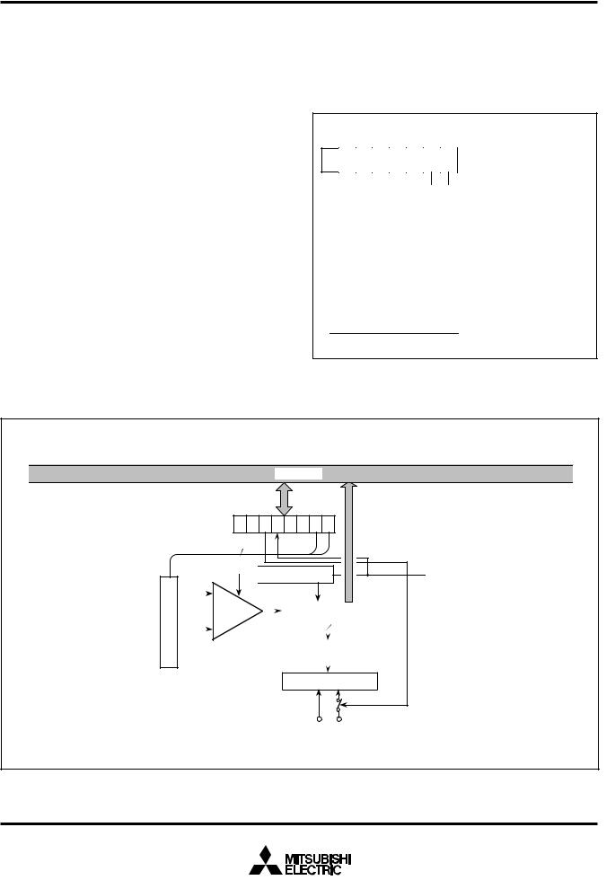
MITSUBISHI MICROCOMPUTERS
M37271MF-XXXSP
M37271EF-XXXSP, M37271EFSP
SINGLE-CHIP 8-BIT CMOS MICROCOMPUTER with CLOSED CAPTION DECODER and ON-SCREEN DISPLAY CONTROLLER
A-D CONVERTER
(1)A-D Conversion Register (AD)
A-D conversion reigister is a read-only register that stores the result of an A-D conversion. This register should not be read during A-D conversion.
(5)Comparator and Control Circuit
The conversion result of the analog input voltage and the reference voltage “Vref” is stored in the A-D conversion register. The A-D conversion completion bit and A-D conversion interrupt request bit are set to “1” at the completion of A-D conversion.
(2)A-D Control Register (ADCON)
The A-D control register controls A-D conversion. Bits 1 and 0 of this register select analog input pins. When these pins are not used as anlog input pins, they are used as ordinary I/O pins. Bit 3 is the A-D conversion completion bit, A-D conversion is started by writing “0” to this bit. The value of this bit remains at “0” during an A-D conversion, then changes to “1” when the A-D conversion is completed.
Bit 4 controls connection between the resistor ladder and VCC. When not using the A-D converter, the resistor ladder can be cut off from the internal VCC by setting this bit to “0.” This can realize the lowpower dissipation.
(3)Comparison Voltage Generator (Resistor Ladder)
The voltage generator divides the voltage between VSS and VCC by 256, and outputs the divided voltages to the comparator as the reference voltage Vref.
(4)Channel Selector
The channel selector connects an analog input pin selected by bits 1 and 0 of the A-D control register to the comparator.
7 |
0 |
0
A-D control register (ADCON: address 00EF16)
Analog input pin selection bits b1 b0
00 : P26/AD1
01 : P25/AD2
10 : P24/AD3
11 : P40/AD4
A-D conversion completion bit 0 : Conversion in purogress
1 : Conversion completed
VCC connection selection bit 0 : OFF
1 : ON
Fix this bit to “0.”
Fig. 18. Structure of A-D control register
Data bus
b7 |
b0 |
A-D control register (address 00EF16)
2
 A-D control circuit
P25/AD2 |
|
selector |
|
|
rator |
|
|
|
||
P26/AD1 |
|
|
|
|
Compa- |
|
|
|
||
|
|
|
|
|
A-D conversion register |
|
||||
|
|
|
|
|
|
|
|
|
||
|
|
|
|
|
|
|
|
|
|
|
|
|
|
|
|
|
|
|
|
|
|
P24/AD3 |
|
Channel |
|
|
|
|
8 |
(address 00EE16) |
||
P40/AD4 |
|
|
|
|
|
|
|
Switch tree |
|
|
|
|
|
|
|
|
|
|
|||
|
|
|
|
|
|
|
|
|
|
|
|
|
|
|
|
|
|
|
|
|
|
 A-D conversion interrupt request
Resistor ladder
VSS VCC
Fig. 19. A-D comparator block diagram
26
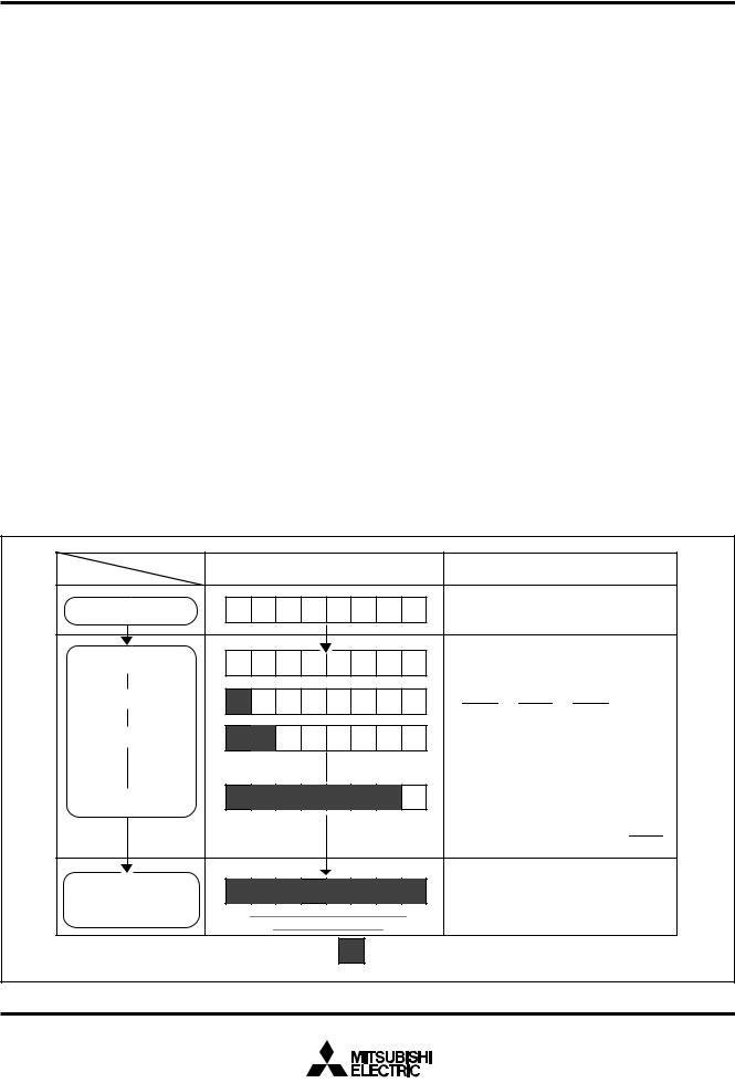
MITSUBISHI MICROCOMPUTERS
M37271MF-XXXSP
M37271EF-XXXSP, M37271EFSP
SINGLE-CHIP 8-BIT CMOS MICROCOMPUTER with CLOSED CAPTION DECODER and ON-SCREEN DISPLAY CONTROLLER
(6) Conversion Method
1Set bit 7 of the interrupt interval determination control register (address 021216) to “1” to generate an interrupt request at completion of A-D conversion.
2Set the A-D conversion · INT3 interrupt request bit to “0” (even when A-D conversion is started, the A-D conversion · INT3 interrupt bit is not set to “0” automatically).
3When using A-D conversion interrupt, enable interrupts by setting A-D conversion · INT3 interrupt request bit to “1” and setting the interrupt disable flag to “0.”
4Set the VCC connection selection bit to “1” to connect VCC to the resistor ladder.
5Select analog input pins by setting the analog input selection bit of the A-D control register.
6Set the A-D conversion completion bit to “0.” This write operation starts the A-D conversion. Do not read the A-D conversion register during the A-D conversion.
7Verify the completion of the conversion by the state (“1”) of the A-D conversion completion bit, that (“1”) of A-D conversion · INT3 interrupt bit, or the occurrence of an A-D conversion interrupt.
8Read the A-D conversion register to obtain the conversion results.
Note : When the ladder resistor is disconnect from VCC, set the VCC connection selection bit to “0” between steps 7and 8.
(7) Internal Operation
At the time when the A-D conversion starts, the following operations are automatically performed.
1The A-D conversion register is set to “0016.”
2The most significant bit of the A-D conversion register becomes
“1, ” and the comparison voltage “Vref” is input to the comparator.
At this point, Vref is compared with the analog input voltage “VIN .” 3Bit 7 is determined by the comparison result as follows.
When Vref < VIN : bit 7 holds “1”
When Vref > VIN : bit 7 becomes “0”
With the above operations, the analog value is converted into a digital value. The A-D conversion terminates in a maximum 50 machine cycles (12.5 μs at f(XIN) = 8 MHz) after it starts, and the conversion result is stored in the A-D conversion register.
An A-D conversion interrupt request occurs at the same time of A-D conversion completion, the A-D conversion · INT3 interrupt request bit becomes “1.” The A-D conversion completion bit also becomes
“1.”
Table 2. Expression for Vref and VREF
A-D conversion register contents “n” |
Vref (V) |
|
(decimal notation) |
||
|
||
|
|
|
0 |
0 |
|
|
|
|
1 to 255 |
VREF (n – 0.5) |
|
|
256 |
|
|
|
|
Note: VREF indicates the voltage of internal VCC. |
|
|
Contents of A-D conversion register |
Reference voltage (V ref) [V] |
||||||||||||
A-D conversion start |
0 |
0 |
0 |
0 |
0 |
0 |
0 |
0 |
|
|
|
0 |
|
|
1st comparison start |
1 |
0 |
0 |
0 |
0 |
0 |
0 |
0 |
VREF – VREF |
|
|
|
||
|
|
|
|
|
|
|
|
|
2 |
|
512 |
|
|
|
2nd comparison start |
1 |
1 |
0 |
0 |
0 |
0 |
0 |
0 |
VREF |
± |
VREF |
– |
VREF |
|
2 |
4 |
512 |
|
|||||||||||
|
|
|||||||||||||
3rd comparison start |
1 |
2 |
1 |
0 |
0 |
0 |
0 |
0 |
VREF ± VREF ± VREF – VREF |
|||||
|
|
|
|
|
|
|
|
|
2 |
|
4 |
|
8 |
512 |
8th comparison start |
1 |
2 |
3 |
4 |
5 |
6 |
7 |
1 |
VREF ± VREF ± VREF ± ..... |
|||||
|
|
|
|
|
|
|
|
|
2 |
|
4 |
|
8 |
|
|
|
|
|
|
|
|
|
|
|
|
....... |
± |
VREF – VREF |
|
|
|
|
|
|
|
|
|
|
|
|
|
|
256 |
512 |
A-D conversion completion |
1 |
2 |
3 |
4 |
5 |
6 |
7 |
8 |
|
|
|
|
|
|
(8th comparison completion) |
|
|
|
|
|
|
||||||||
|
Digital value corresponding to |
|
|
|
|
|
|
|
||||||
|
|
|
|
|
|
|
|
|
||||||
|
|
|
analog input voltage. |
|
|
|
|
|
|
|
|
|||
m : Value determined by mth (m = 1 to 8) result
Fig. 20. Changes in A-D conversion register and comparison voltage during A-D conversion
27
MITSUBISHI MICROCOMPUTERS
M37271MF-XXXSP
M37271EF-XXXSP, M37271EFSP
SINGLE-CHIP 8-BIT CMOS MICROCOMPUTER with CLOSED CAPTION DECODER and ON-SCREEN DISPLAY CONTROLLER
(8) Definition of A-D Conversion Accuracy
The definition of A-D conversion accuracy is described below.
1Relative accuracy
· Zero transition error (V0T)
The deviation of the input voltage at which A-D conversion output data changes from “0” to “1,” from the corresponding ideal A-D conversion characteristics between 0 and VREF.
V0T = |
(V0 –1/2 VREF/256) |
[LSB] |
|
1LSB |
|||
|
|
· Full-scale transition error (VFST)
The deviation of the input voltage at which A-D conversion output data changes from “255” to “254,” from the corresponding ideal A-
D conversion characteristics between 0 and VREF.
(VREF – 3/2 VREF/256) – V254
VFST = |
|
[LSB] |
|
1LSB |
|||
|
|||
|
|
· Non-linearity error
The deviation of the actual A-D conversion characteristics, from the ideal A-D conversion characteristics between V0 and V254.
Non-linearity error = |
Vn – (1LSB n + V0) |
|
|
[LSB] |
|
|
||
|
1LSB |
|
· Differential non-linearity error
The deviation of the input voltage required to change output data by “1,” from the corresponding ideal A-D conversion characteristics between 0 and VREF.
|
(Vn+1 – Vn) – 1LSB |
|
Differential non-linearity error = |
|
[LSB] |
|
||
|
1LSB |
|
2Absolute accuracy |
|
|
· Absolute accuracy error
The deviation of the actual A-D conversion characteristics, from the ideal A-D conversion characteristics between 0 and VREF.
Absolute accuracy error = |
Vn – 1LSBA (n+1/2) |
|
|
|
[LSB] |
||
1LSBA |
|||
|
|||
|
|
Note: The analog input voltage “Vn” at which A-D conversion output data changes from “n” to “n + 1” (n ; 0 to 254) is as follows (refer to Figure 18).
1LSB with respect to relative accuracy = |
|
V254 – V0 |
|
[V] |
|
254 |
|
||
|
|
|
|
|
1LSBA with respect to absolute accuracy = |
VREF |
|
|
|
|
|
[V] |
||
256 |
|
|||
|
|
|
|
|
Output |
|
|
|
|
data |
|
|
|
|
255 |
|
|
|
|
254 |
Full-scale transition error |
|
|
|
(VFST) |
|
|
|
|
|
|
|
|
|
|
|
Differential non- |
3 |
LSBA |
|
|
2 |
||
|
|
linearity error |
||
|
|
|
|
|
|
|
1LSB |
|
|
n+1 |
|
|
|
|
n |
|
|
|
|
Actual A-D |
Non-linearity error |
|
||
conversion |
|
Absolute accuracy |
|
|
characteristics |
|
|
||
|
|
|
||
|
1LSB A |
|
|
|
1 |
LSBA |
Ideal A-D conversion characteristics |
||
2 |
|
between V0 and V254 |
|
|
|
|
|
||
|
|
1LSB |
|
|
0 |
V0 V1 |
Vn Vn+1 |
V254 |
VREF |
Zero transition error (V 0T)
Analog input voltage (V)
Fig. 21. Definition of A-D conversion precision
28

MITSUBISHI MICROCOMPUTERS
M37271MF-XXXSP
M37271EF-XXXSP, M37271EFSP
SINGLE-CHIP 8-BIT CMOS MICROCOMPUTER with CLOSED CAPTION DECODER and ON-SCREEN DISPLAY CONTROLLER
DATA SLICER
The M37271MF-XXXSP includes the data slicer function for the closed caption decoder (referred to as the CCD). This function takes out the caption data superimposed in the vertical blanking interval of a composite video signal. A composite video signal which makes the sync chip’s polarity negative is input to the CVIN pin.
When the data slicer function is not used, the data slicer circuit can be cut off by setting bit 0 of the data slicer control register 1 (address 00EA16) to “0.” Also, the timing signal generating circuit can be cut off by setting bit 0 of data slicer control register 2 (address 00EB16) to “0.” These settings can realize the low-power dissipation.
Composite |
|
|
|
|
|
|
|
|
0.1µF |
|
470Ω |
|
|
|
|
|
|
|
|
|
|
|
|
|
|
|
|
|
|
1 kΩ |
15 kΩ |
|
|
|
|
|
|
|
|
|
|
|
|
|
|
|
|
|
|
||||||||||||||||||||||||||||||||||||||||||||||||
video |
|
|
|
|
|
|
|
|
|
|
|
|
|
|
|
|
|
|
|
|
|
|
|
|
|
|
|
|
|
|
|
|
|
|
|
|
|
|
|
|
|
|
|
|
|
|
|
|
|
|
|
|
|
|
|
|
|
|
|
|
|
|
|||||||||||||||||||||||||||||||||||
|
|
|
|
|
|
|
|
|
|
|
|
|
|
|
|
|
|
|
|
|
|
|
|
|
|
|
|
|
|
|
|
|
|
|
560 pF |
|
|
|
|
|
|
|
|
|
|
|
|
|
|
|
|
|
|
|
|
|
|
|
|
|
|
|
|
|
|
|
|
|
|
|
|
Sync pulse counter |
|
||||||||||||||||||||||||
signal |
|
|
|
|
|
Hundred of kiloohms |
|
|
|
|
|
|
|
|
|
|
1µF |
|
|
|
|
|
200 pF |
|
|
|
|
|
|
|
|
|
|
|
|
|
|
|
|
|
|
|
|
|
|||||||||||||||||||||||||||||||||||||||||||||||||||||
|
|
|
|
|
|
|
|
|
|
|
|
|
|
|
|
|
|
|
|
|
|
|
|
|
|
|
|
|
|
|
|
|
|
|
|
|
|
|
|
register |
|
|
|
|
|
|
|
|
|
|
|
|
|||||||||||||||||||||||||||||||||||||||||||||
|
|
|
|
|
|
|
|
|
|
|
|
|
|
|
|
|
|
|
|
|
|
|
|
|
|
|
|
|
|
|
|
|
|
|
|
|
|
|
|
|
|
|
|
|
|
|
|
|
|
|
|
|
|
|
|
|
|
|
|
||||||||||||||||||||||||||||||||||||||
|
|
|
|
|
|
|
to 1 MΩ |
|
|
|
|
|
|
|
|
|
|
|
|
|
|
|
|
|
|
|
|
|
|
|
|
|
|
|
|
|
|
|
|
|
|
|
|
|
|
|
|
|
|
|
|
|
|
|
|
|
|
|
|
(address 020F16) |
|
||||||||||||||||||||||||||||||||||||
|
|
|
|
|
|
|
|
|
|
|
|
|
|
|
|
|
|
|
|
|
|
|
|
|
|
|
|
|
|
|
|
|
CVIN |
|
|
|
|
|
|
HSYNC |
|
|
|
|
|
|
|
|
|
|
|
|
|
|
HLF |
|
|
|
|
RVCO |
|
|
|
|
|
|
|
|
|
|
|
|
|
|
|
|
|
|
|
||||||||||||||||||
|
|
|
|
|
|
|
|
|
|
|
|
|
|
|
|
|
|
|
|
|
|
|
|
|
|
|
|
|
|
|
|
|
|
|
|
|
|
|
|
|
|
|
|
|
|
|
|
|
|
|
|
|
|
|
|
|
|
|
|
|
|
|
|
|
|
|
|
|
|
|
|
|
|
|
|
||||||||||||||||||||||
|
|
|
|
|
|
|
|
|
|
|
|
|
|
|
|
|
|
|
|
|
|
|
|
|
|
|
|
|
|
|
|
|
|
|
|
|
|
|
|
|
|
|
|
|
|
|
|
|
|
|
|
|
|
|
|
|
|
|
|
|
|
|
|
|
|
|
|
|
|
|
|
|
|
|
|
|
|
|
|
|
|
|
|
|
|
|
|
|
|
|
|
||||||
|
|
|
|
|
|
|
|
|
|
|
|
|
|
|
|
|
|
|
|
|
|
|
|
|
|
|
|
|
|
|
|
|
|
|
|
|
|
|
|
|
|
|
|
|
|
|
|
|
|
|
|
|
|
|
|
|
|
|
|
|
|
|
|
|
|
|
|
|
|
|
|
|
|
|
|
|
|
|
Clock run-in register 2 |
|
|||||||||||||||||
|
|
|
|
|
|
|
|
|
|
|
|
|
|
|
|
|
|
|
|
|
|
|
|
|
|
|
|
|
|
|
|
|
|
|
|
|
|
|
|
|
|
|
|
|
|
|
|
|
|
|
|
|
|
|
|
|
|
|
|
|
|
|
|
|
|
|
|
|
|
|
|||||||||||||||||||||||||||
|
|
|
|
|
|
|
|
|
|
|
|
|
|
|
|
|
|
|
|
|
|
|
|
|
|
|
|
|
|
|
|
|
|
|
|
|
|
|
|
|
|
|
|
|
|
|
|
Synchronizing |
|
|
|
|
|
|
|
|
|
|
|
|
|
|
|
|
|
(address 00E716) |
|
||||||||||||||||||||||||||||||
|
|
|
|
|
|
|
|
|
|
|
|
|
|
|
|
|
|
|
|
|
|
|
|
|
|
|
|
|
|
|
|
|
|
|
|
|
|
|
|
|
|
|
|
|
|
|
|
|
|
|
|
|
|
|
|
|
|
|
|
|
|
|
|
|
|
||||||||||||||||||||||||||||||||
|
|
|
|
|
|
|
|
|
|
|
|
|
|
|
|
|
|
|
|
|
|
|
|
|
|
|
|
|
|
|
|
|
|
|
|
|
|
|
|
|
|
|
|
|
|
|
|
signal counter |
|
|
|
|
|
|
|
|
|
|
|
|
|
|
|
1 |
0 |
0 |
1 |
1 |
1 |
|
|
|
|
|
|
||||||||||||||||||||||
|
|
|
|
|
|
|
|
|
|
|
|
|
|
|
|
|
|
|
|
|
|
|
|
|
|
|
|
|
|
|
|
|
|
|
|
|
|
|
|
|
|
|
|
|
|
|
|
|
|
|
|
|
|
|
|
|
|
|
|
|
|
|
|
|
|
|
|
|
|
|
|||||||||||||||||||||||||||
|
|
|
|
|
|
|
|
|
|
|
|
|
|
|
|
|
|
|
|
|
|
|
|
|
|
|
|
|
|
|
Clamping |
|
|
|
|
|
|
|
|
|
|
|
|
|
|
|
|
|
|
|
|
|
|
|
|
|
|
|
|
|
|
|
|
|
|
|
|
|
|
|
|
|
|
|
|
|
|
|
|
|
|
|
|
|
|
|
|
|
|
|
|
||||||
|
|
|
|
|
|
|
|
|
|
|
|
|
|
|
|
|
|
|
|
|
|
|
|
|
|
|
|
|
|
|
|
|
|
|
|
|
|
|
|
|
|
|
|
|
|
|
|
|
|
|
|
|
|
|
|
|
|
|
|
|
|
|
|
|
|
|
Data slicer control register 2 |
|
|||||||||||||||||||||||||||||
|
|
|
|
|
|
|
|
|
|
|
|
|
|
|
|
|
|
|
|
|
|
|
|
|
|
|
|
|
|
|
circuit |
|
|
|
|
|
|
|
|
|
|
|
|
|
|
|
|
|
|
|
|
|
|
|
|
|
|
|
|
|
|
|
|
|
|
|
|
|
|
|
|
||||||||||||||||||||||||||
|
|
|
|
|
|
|
|
|
|
|
|
|
|
|
|
|
|
|
|
|
|
|
|
|
|
|
|
|
|
|
|
|
|
|
|
|
|
|
|
|
|
|
|
|
|
|
|
|
|
|
|
|
|
|
|
|
|
|
|
|
|
|
|
|
|
|
|
|
|
(address 00EB16) |
|
||||||||||||||||||||||||||
|
|
|
|
|
|
|
|
|
|
|
|
|
|
|
|
|
|
|
|
|
|
|
|
|
|
|
|
|
|
|
|
|
|
|
|
|
|
|
|
|
|
|
|
|
|
|
|
|
|
|
|
|
|
|
|
|
|
|
|
|
|
|
|
|
|
|
|
|
|
|
|
|
|
|
|
||||||||||||||||||||||
|
|
|
|
|
|
|
|
|
|
|
|
|
|
|
|
|
|
|
|
|
|
|
|
|
|
|
|
|
|
|
|
|
|
|
|
|
|
|
|
|
|
|
|
|
|
|
|
|
|
|
|
|
|
|
|
|
|
|
|
|
|
|
|
|
|
|
|
|
|
|
|
|
|
|
|
|
|
|
|
0 |
|
|
|
|
0 |
0 |
|
|
|
|
|
|
|
|
|||
|
|
|
|
|
|
|
|
|
|
|
|
|
|
|
|
|
|
|
Low-pass |
|
|
|
|
|
|
Sync slice |
|
|
Synchronizing |
|
|
|
|
|
|
|
|
|
|
|
|
|
|
|
|
|
|
|
|
|
|
|
|
|
|
|
|
|
|
|
|
|
|
|
|
|
|
|
|
|
|||||||||||||||||||||||||||
|
|
|
|
|
|
|
|
|
|
|
|
|
|
|
|
|
|
|
|
|
|
|
|
|
|
|
separation |
|
|
|
|
|
|
|
|
|
|
|
|
|
|
|
|
|
|
|
|
|
|
|
|
|
|
|
|
|
|
|
|
|
|
|
|
|
|
|
|
|
|||||||||||||||||||||||||||||
|
|
|
|
|
|
|
|
|
|
|
|
|
|
|
|
|
|
|
filter |
|
|
|
|
|
|
|
|
|
circuit |
|
|
|
|
|
circuit |
|
|
|
|
|
|
|
|
|
|
|
|
|
|
|
|
|
|
|
Data slicer control register 1 |
|
|||||||||||||||||||||||||||||||||||||||||
|
|
|
|
|
|
|
|
|
|
|
|
|
|
|
|
|
|
|
|
|
|
|
|
|
|
|
|
|
|
|
|
|
|
|
|
|
|
|
|
|
|
|
|
|
|
|
|
|
|
|
|
|
|
|
|
|
|
|
|
|
|
|
|
|
|||||||||||||||||||||||||||||||||
|
|
|
|
|
|
|
|
|
|
|
|
|
|
|
|
|
|
|
|
|
|
|
|
|
|
|
|
|
|
|
|
|
|
|
|
|
|
|
|
|
|
|
|
|
|
|
|
|
|
|
|
|
|
|
|
|
|
|
|
|
|
|
|
|
|
|
|
|
|
|
|
|
|
|
|
(address 00EA16) |
|
||||||||||||||||||||
|
|
|
|
|
|
|
|
|
|
|
|
|
|
|
|
|
|
|
|
|
|
|
|
|
|
|
|
|
|
|
|
|
|
|
|
|
|
|
|
|
|
|
|
|
|
|
|
|
|
|
|
|
|
|
|
|
|
Timing signal |
|
|
|
|
|
|
|
|
|
|
0 |
|
|
|
|
0 |
0 |
|
|
|
|
|
|
|
|
||||||||||||||
|
|
|
|
|
|
|
|
|
|
|
|
|
|
|
|
|
|
|
|
|
|
|
|
|
|
|
|
|
|
|
|
|
|
|
|
|
|
|
|
|
|
|
|
|
|
|
|
|
|
|
|
|
|
|
|
|
|
|
|
|
|
|
|
|
|
|
|
|
|
|
|
|
|
|
|
|
|
|
|
||||||||||||||||||
|
|
|
|
|
|
|
|
|
|
|
|
|
|
|
|
|
|
|
|
|
|
|
|
|
|
|
|
|
|
|
|
|
|
|
|
|
|
|
|
|
|
|
|
|
|
|
|
|
|
|
|
|
|
|
|
|
|
generating |
|
|
|
|
|
|
|
|
|
|
|
|
|
|
|
|
|
|
|
|
|
|
|
|
|
|
|
|
|||||||||||
|
|
|
|
|
|
|
|
|
|
|
|
|
|
|
|
|
|
|
|
|
|
|
|
|
|
|
|
|
|
|
|
|
|
|
|
|
|
|
|
|
|
|
|
|
|
|
|
|
|
|
|
|
|
|
|
|
|
circuit |
|
|
|
|
|
|
|
|
|
|
Data slicer ON/OFF |
|
|||||||||||||||||||||||||||
|
|
|
|
|
|
|
|
|
|
|
|
|
|
|
|
|
|
|
|
|
|
|
|
|
|
|
|
|
|
|
|
|
|
|
|
|
|
|
|
|
|
|
|
|
|
|
|
|
|
|
|
|
|
|
|
|
|
|
|
|
|
|
|
|
|
|
|
|
|
|
|
|
|
|
|
|
|
Window register |
|
||||||||||||||||||
|
|
|
|
|
|
|
|
|
|
|
|
|
|
|
|
|
|
|
|
|
|
|
|
|
|
|
|
|
|
|
|
|
|
|
|
|
|
|
|
|
|
|
|
|
|
|
|
|
|
|
|
|
|
|
|
|
|
|
|
|
|
|
|
|
|
|
|
|
|
|
|||||||||||||||||||||||||||
|
|
|
|
|
|
|
VHOLD |
|
Reference |
|
|
|
|
|
|
|
|
|
|
|
|
|
|
|
|
|
|
|
|
|
|
|
|
|
|
|
|
|
|
|
|
|
|
|
|
|
|
|
|
|
|
|
|
|
|
|
|
|
|
|
|
|
|
(address 00E216) |
|
||||||||||||||||||||||||||||||||
|
|
|
|
|
|
|
|
|
|
|
|
|
|
|
|
|
|
|
|
|
|
|
|
|
|
|
|
|
|
|
|
|
|
|
|
|
|
|
|
|
|
|
|
|
|
|
|
|
|
|
|
|
|
|
|
|
|
|
|
|
|
|
|
|
|
|
|
|
|
|
|
|
|
|
|
|
|
|
|
|
|||||||||||||||||
|
|
|
|
|
|
|
|
|
|
|
|
|
voltage |
|
|
|
|
|
|
|
|
|
|
|
|
+ |
|
|
|
|
|
|
|
|
|
|
|
|
|
|
|
|
|
|
|
|
|
|
|
|
|
|
|
|
|
|
|
|
|
|
|
|
|
|
|
|
|
|
0 |
0 |
|
|
|
|
|
|
|
|
|
|
|
|
|
|
|
|
|||||||||||
|
|
|
|
|
|
|
1000 pF |
|
generating |
|
|
|
|
|
|
|
|
|
|
|
|
|
|
|
|
|
|
|
|
|
|
|
|
|
|
|
|
|
|
|
|
|
|
|
Clock run-in |
|
|
|
|
|
|
|
|
|
|
|
|
|
|
|
|
|
|
|
|
|
|
|
|
|
|
|
|
||||||||||||||||||||||||
|
|
|
|
|
|
|
|
|
|
|
|
|
|
|
|
|
|
|
|
|
|
|
|
|
|
|
|
|
|
|
|
|
|
|
|
|
|
|
|
|
|
|
|
|
|
|
|
|
|
|
|
|
|
|
|
|
|
|
|
|
|
|
|
|
|
||||||||||||||||||||||||||||||||
|
|
|
|
|
|
|
|
circuit |
|
|
|
|
|
|
|
|
|
|
|
|
– |
|
|
|
|
|
|
|
|
|
|
|
|
|
|
|
|
|
|
|
|
|
|
determination |
|
|
|
|
|
|
|
|
|
|
|
|
|
|
|
|
|
|
|
|
|
|
|
|
|
|
|
|
|||||||||||||||||||||||||
|
|
|
|
|
|
|
|
|
|
|
|
|
|
|
|
|
|
|
|
|
|
|
|
|
|
|
|
|
|
|
|
|
|
|
|
|
|
|
|
|
|
|
|
|
|
|
|
|
|
|
|
|
|
|
|
|
|
|
circuit |
|
|
|
|
|
|
|
0 |
1 |
0 |
|
1 |
|
|
|
|
|
|
|
|
|
|
||||||||||||||||
|
|
|
|
|
|
|
|
|
|
|
|
|
|
|
|
|
|
|
|
|
|
|
|
|
|
|
|
|
|
Comparator |
|
|
|
|
|
|
|
|
|
|
|
|
|
|
|
|
|
|
|
|
|
|
|
|
|
|
|
|
|
|
|
|
|
|
|
|
|
|
|
||||||||||||||||||||||||||||
|
|
|
|
|
|
|
|
|
|
|
|
|
|
|
|
|
|
|
|
|
|
|
|
|
|
|
|
|
|
|
|
|
|
|
|
|
|
|
|
|
|
|
|
|
|
|
|
|
|
|
|
|
|
|
|
|
|
|
|
|
|
|
|
|
|
|
|
|
Clock run-in register 1 |
|
|||||||||||||||||||||||||||
|
|
|
|
|
|
|
|
|
|
|
|
|
|
|
|
|
|
|
|
|
|
|
|
|
|
|
|
|
|
|
|
|
|
|
|
|
|
|
|
|
|
|
|
|
|
|
|
|
|
|
|
|
|
|
|
|
|
|
|
|
|
|
|
|
|
|
|
|
|
||||||||||||||||||||||||||||
|
|
|
|
|
|
|
|
|
|
|
|
|
|
|
|
|
|
|
|
|
|
|
|
|
|
|
|
|
|
|
|
|
|
|
|
|
|
|
|
|
|
|
|
|
|
|
|
|
Data slice line |
|
|
|
|
|
|
|
|
|
|
|
|
|
|
|
|
|
(address 00E616) |
|
|||||||||||||||||||||||||||||
|
|
|
|
|
|
|
|
|
|
|
|
|
|
|
|
|
|
|
|
|
|
|
|
|
|
|
|
|
|
|
|
|
|
|
|
|
|
|
|
|
|
|
|
|
|
|
|
|
|
|
|
|
|
|
|
|
|
|
|
|
|
|
|
|
|
|
|
||||||||||||||||||||||||||||||
|
|
|
|
|
|
|
|
|
|
|
|
|
|
|
|
|
|
|
|
|
|
|
|
|
|
|
|
|
|
|
|
|
|
|
|
|
|
|
|
|
|
|
|
|
|
|
|
|
specification |
|
|
|
|
|
|
|
|
|
|
|
|
|
|
|
|
|
|
|
|
|
|
|
|
|
|
|
|
|
|
|
|
|
|
|
|
||||||||||||
|
|
|
|
|
|
|
|
|
|
|
|
|
|
|
|
|
|
|
|
|
|
|
|
|
|
|
|
|
|
|
|
|
|
|
|
|
|
|
|
|
|
|
|
|
|
|
|
|
|
|
|
|
|
|
|
|
|
|
|
|
|
|
|
|
|
|
|
|
|
|
|
|
|
|
|
|
|||||||||||||||||||||
|
|
|
|
|
|
|
|
|
|
|
|
|
|
|
|
|
|
|
|
|
|
|
|
|
|
|
Data slicer control |
|
|
|
|
|
|
|
|
|
circuit |
|
|
|
|
|
|
|
|
|
|
|
|
|
|
|
|
|
|
|
|
|
|
|
|
|
|
|
|
|
|
|
|
|
|
|
|
|
|
|
|
|
|||||||||||||||||||
|
|
|
|
|
|
|
|
|
|
|
|
|
|
|
|
|
|
|
|
|
|
|
|
|
|
|
|
|
|
|
|
|
|
|
|
|
|
|
|
|
|
|
|
|
|
|
|
|
|
|
|
|
|
|
|
|
|
|
|
|
|
|
|
|
|
1 |
0 |
0 |
|
|
|
|
|
|
|
|
|
|
|
|
|
||||||||||||||||
|
|
|
|
|
|
|
|
|
|
|
|
|
|
|
|
|
|
|
|
|
|
|
|
|
|
|
register 3 |
|
|
|
|
|
|
|
|
|
|
|
|
|
|
|
|
|
|
|
|
|
|
|
|
|
|
|
|
|
|
|
|
|
|
|
|
|
|
|
|
|
|
|
|
|
|
|
|
|
|
|
|
|
|
|
|
|
|
|
|
|
|
||||||||
|
|
|
|
|
|
|
|
|
|
|
|
|
|
|
|
|
|
|
|
|
|
|
|
|
|
|
|
|
|
|
|
|
|
|
|
|
|
|
|
|
|
|
|
|
|
|
|
|
|
|
|
|
|
|
|
|
|
|
|
|
|
|
|
|
|
|
|
|
Caption position register |
|
|||||||||||||||||||||||||||
|
|
|
|
|
|
|
|
|
|
|
|
|
|
|
|
|
|
|
|
|
|
|
|
|
|
|
(address 021016) |
|
|
|
|
|
|
|
|
|
Start bit detecting |
|
|
|
|
|
|
|
|
|
|
|
|
|
|
(address 00E016) |
|
||||||||||||||||||||||||||||||||||||||||||||
|
|
|
|
|
|
|
|
|
|
|
|
|
|
|
|
|
|
|
|
|
|
|
|
|
|
|
|
|
|
|
|
|
|
|
|
|
|
|
|
|
|
|
|
|
|
|
|
|
|
|
|
|
|
|
|
|
|
|
|
|
|
|
|
||||||||||||||||||||||||||||||||||
|
|
|
|
|
|
|
|
|
|
|
|
|
|
|
|
|
|
|
|
|
|
|
|
|
|
|
|
|
|
|
|
|
|
|
|
|
|
|
|
|
|
|
|
|
|
|
|
|
|
|
|
|
|
|
|
|
|
|
|
|
|
|
|
|
|
|
|
|
|
|
|
|
|
|
|
|
|
|
|
|
|
||||||||||||||||
|
|
|
|
|
|
|
|
|
|
|
|
|
|
|
|
|
|
|
|
|
|
|
|
|
|
|
Clock run-in detect |
|
|
|
|
|
|
|
|
|
circuit |
|
|
|
|
|
|
|
|
|
|
|
|
|
|
|
|
|
|
|
|
|
|
|
|
|
|
|
|
|
|
|
|
|
|
|
|
|
|
|
|
|
|||||||||||||||||||
|
|
|
|
|
|
|
|
|
|
|
|
|
|
|
|
|
|
|
|
|
|
|
|
|
|
|
register 3 |
|
|
|
|
|
|
|
|
|
|
|
|
|
|
|
|
|
|
|
|
|
|
|
|
|
|
|
|
|
|
|
|
|
|
|
|
|
|
|
|
|
|
|
|
|
|
|
|
|
|
|
|
|
|
|
|
|
|
|
|
|
|
||||||||
|
|
|
|
|
|
|
|
|
|
|
|
|
|
|
|
|
|
|
|
|
|
|
|
|
|
|
|
|
|
|
|
|
|
|
|
|
|
|
|
|
|
|
|
|
|
|
|
|
|
|
|
|
|
|
|
|
|
|
|
|
|
|
|
|
|
|
|
|
|
|
|
|
|
|
|
|
|
|
|
|
|
|
|
|
|
|
|
|
|||||||||
|
|
|
|
|
|
|
|
|
|
|
|
|
|
|
|
|
|
|
|
|
|
|
|
|
|
|
(address 020816) |
|
|
|
|
|
|
|
|
|
|
|
|
|
|
|
|
|
|
|
|
|
|
|
|
|
|
|
|
|
|
|
|
|
|
|
|
|
|
Start bit position register |
|
||||||||||||||||||||||||||||||
|
|
|
|
|
|
|
|
|
|
|
|
|
|
|
|
|
|
|
|
|
|
|
|
|
|
|
|
|
|
|
|
|
|
|
|
|
|
|
|
|
|
|
|
|
|
|
|
|
|
|
|
|
|
|
|
|
|
|
|
|
|
|
|
|
|||||||||||||||||||||||||||||||||
|
|
|
|
|
|
|
|
|
|
|
|
|
|
|
|
|
|
|
|
|
|
|
|
|
|
|
|
|
|
|
|
|
|
|
|
|
|
|
|
|
|
|
|
|
|
|
|
Data clock |
|
|
|
|
|
|
|
|
|
|
|
|
|
|
(address 00E116) |
|
|||||||||||||||||||||||||||||||||
|
|
|
|
|
|
|
|
|
|
|
|
|
|
|
|
|
|
|
|
|
|
|
|
|
|
|
Clock run-in |
|
|
|
|
|
|
|
|
|
|
|
|
generating circuit |
|
|
|
|
|
|
|
|
|
|
|
|
|
|
|
|
|
|
|
|
|
|
|
|
|
|
|
|
|
|
|
|
|
|
|||||||||||||||||||||||
|
|
|
|
|
|
|
|
|
|
|
|
|
|
|
|
|
|
|
|
|
|
|
|
|
|
|
register 3 |
|
|
|
|
|
|
|
|
|
|
|
|
|
|
|
|
|
|
|
|
|
|
|
|
|
|
|
|
|
|
|
|
|
|
|
|
|
|
|
|
|
|
|
|
|
|
|
|
|
|
|
|
|
|
|
|
|
|
|
|
|
|
||||||||
|
|
|
|
|
|
|
|
|
|
|
|
|
|
|
|
|
|
|
|
|
|
|
|
|
|
|
(address 020916) |
|
|
|
|
|
|
|
|
|
|
|
|
|
|
|
|
|
|
|
|
|
|
|
|
|
|
|
|
|
|
|
|
|
|
|
|
|
|
|
|
|
|
|
|
|
|
|
|
|
|
|
|
|
|
|
|
|
|
||||||||||||
|
|
|
|
|
|
|
|
|
|
|
|
|
|
|
|
|
|
|
|
|
|
|
|
|
|
|
|
|
|
|
|
|
|
|
|
|
|
|
|
|
|
|
|
|
|
|
|
|
|
|
|
|
|
|
|
|
|
|
|
|
|
|
|
|
|
|
|
|
|
|
|
|
|
|
|
|
|
|
|
|
|
|
|
|
|
|
|
|
|||||||||
|
|
|
|
|
|
|
|
|
|
|
|
|
|
|
|
|
|
|
|
|
|
|
|
|
|
|
|
|
|
|
|
|
|
|
|
|
|
|
|
|
|
|
|
|
|
|
|
|
|
|
|
|
|
|
|
|
|
|
|
|
|
|
|
|
|
|
|
|
|
|
|
|
|
Clock run-in detect register 1 |
|
||||||||||||||||||||||
|
|
|
|
|
|
|
|
|
|
|
|
|
|
|
|
|
|
|
|
|
|
|
|
|
|
|
|
|
|
|
|
|
|
|
|
|
|
|
|
|
|
|
|
|
|
|
|
|
|
|
|
|
|
|
|
|
|
|
|
|
|
|
|
|
|
|
|
|
|
|
(address 00E816) |
|
|||||||||||||||||||||||||
|
|
|
|
|
External circuit |
|
|
|
|
|
|
|
|
|
|
|
|
|
|
|
|
|
|
|
|
|
|
|
|
|
|
|
|
|
|
|
|
|
|
|
|
|
16-bit shift register |
|
|
|
|
|
|
|
|
|
|
|
|||||||||||||||||||||||||||||||||||||||||||
|
|
|
|
|
|
|
|
|
|
|
|
|
|
|
|
|
|
|
|
|
|
|
|
|
|
|
|
|
|
|
|
|
|
|
|
|
|
|
|
|
|
|
|
|
|
|
|
|
|
|
|
|
|
|
|
|
|
|
|
|
|
|
|
|
|
|
|
|
|
|
|
|
|
|
|
|
|
|
|
|
|
||||||||||||||||
|
Note: Make the length of wiring which is |
|
|
|
|
|
|
|
|
|
|
|
|
|
|
|
|
|
|
|
|
|
|
|
|
|
|
|
|
|
|
|
|
|
|
|
|
|
|
|
|
|
|
|
|
|
|
|
|
|
|
|
|
|
|
|
|
|
|
|
|
|
|
|
|
|
|
|
|
|
|
|
|
||||||||||||||||||||||||
|
|
|
|
|
|
|
|
|
|
|
|
|
|
|
|
|
|
|
|
|
|
|
|
|
|
|
|
|
|
|
|
|
|
|
|
|
|
|
|
|
|
|
|
|
|
|
|
|
|
|
|
|
|
|
|
|
|
|
|
|
|
|
|
|
|
|
|
|
|
|
|||||||||||||||||||||||||||
|
|
connected to VHOLD, HLF, RVCO |
|
|
|
|
|
|
|
|
|
|
|
|
|
|
|
|
|
|
|
high-order |
|
|
|
|
|
|
low-order |
|
|
|
|
|
|
|
|
|
|
|
|
|
|
|
|
|
|
|
|
|
|
|
|
|
|
|
|
||||||||||||||||||||||||||||||||||||||||
|
|
and CVIN pin as short as possible |
|
|
|
Data register 2 |
|
|
|
|
|
|
|
|
|
|
|
|
|
|
|
Clock run-in detect register 2 |
|
||||||||||||||||||||||||||||||||||||||||||||||||||||||||||||||||||||||||||
|
|
|
|
|
|
|
|
|
|
|
|
|
|
|
|
|
|
|
|
|
|
|
|
|
|
|
|
|
|
|
|
|
|
|
|
|
|
|
|
|
|
|
|||||||||||||||||||||||||||||||||||||||||||||||||||||||
|
|
|
|
|
|
|
|
|
|
|
|
|
|
|
|
|
|
|
|
|
|
|
|
|
|
|
|
|
|
|
|
|
|
|
|
|
|
|
|
|
|
||||||||||||||||||||||||||||||||||||||||||||||||||||||||
|
|
so that a leakage current may |
|
|
(address 00E5 |
16) |
|
|
|
|
|
|
|
|
|
|
|
|
|
|
|
|
|
|
|
|
|
|
|
|
|
|
|
|
|
|
|
|
|
|
|
|
(address 00E916) |
|
|||||||||||||||||||||||||||||||||||||||||||||||||||||
|
|
not be generated when mounting |
|
|
|
|
|
|
|
|
|
|
|
|
|
|
|
|
|
|
|
|
|
|
|
|
|
|
|
|
|
|
|
|
|
|
|
|
|
|
|
|
|||||||||||||||||||||||||||||||||||||||||||||||||||||||
|
|
|
|
|
|
|
|
|
|
|
|
|
|
|
|
|
|
|
|
|
|
|
|
|
|
|
|
|
|
|
|
|
|
|
|
|
|
|
|
|
|
|
|
|
|
|
|
|
|
|
|
|
|
|
|
|
|
|
|
|
|
|
|
|
|
|
|
|
|
|
|
|
|
||||||||||||||||||||||||
|
|
a resistor or a capacitor on each |
|
|
|
|
|
|
|
|
|
|
|
|
|
|
|
|
|
|
|
|
|
|
|
|
|
|
|
|
|
|
|
|
Data register 1 |
|
|
|
|
|
|
|
|
|
|
|
|
|
|
|
|
Data slicer |
|
||||||||||||||||||||||||||||||||||||||||||||
|
|
|
|
|
|
|
|
|
|
|
|
|
|
|
|
|
|
|
|
|
|
|
|
|
|
|
|
|
|
|
|
|
|
|
|
|
|
|
|
|
|
|
|
|
|
|
|
|
|
||||||||||||||||||||||||||||||||||||||||||||||||
|
|
pin. |
|
|
|
|
|
|
|
|
|
|
|
|
|
|
|
|
|
|
|
|
|
|
|
|
|
|
|
|
|
|
|
|
|
|
|
|
|
|
|
|
|
|
|
|
|
|
(address 00E416) |
Interrupt request |
|
|
|
|
|
|
|
||||||||||||||||||||||||||||||||||||||||
|
|
|
|
|
|
|
|
|
|
|
|
|
|
|
|
|
|
|
|
|
|
|
|
|
|
|
|
|
|
Data register 4 |
|
|
|
|
|
|
|
|
|
|
|
|
interrupt |
|
|||||||||||||||||||||||||||||||||||||||||||||||||||||
|
|
|
|
|
|
|
|
|
|
|
|
|
|
|
|
|
|
|
|
|
|
|
|
|
|
|
|
|
|
|
|
|
|
|
|
|
|
|
|
|
|
|
|
|
|
|
|
|
|
|
|
|
|
|
|
|
|
generating circuit |
|
|
|
|
|
|
|
||||||||||||||||||||||||||||||||
|
|
|
|
|
|
|
|
|
|
|
|
|
|
|
|
|
|
|
|
|
|
|
|
|
|
|
|
|
|
|
|
|
|
|
|
|
|
|
|
|
|
|
|
|
|
|
|
|
|
|
|
|
|
|
|
|
|
|
|
request |
|
||||||||||||||||||||||||||||||||||||
|
|
|
|
|
|
|
Sync slice register 3 |
|
|
|
|
|
|
|
|
|
|
|
|
|
(address 00ED16) |
|
|
|
|
|
|
|
|
|
|
|
|
|
|
|
|
|
|
|
|
|
|
|
|
|
|
|
|
|
|
|
|
|
|
|
|||||||||||||||||||||||||||||||||||||||||
|
|
|
|
|
|
|
|
|
|
|
|
|
|
|
|
|
|
|
|
|
|
|
|
|
|
|
|
|
|
|
|
|
|
|
|
|
|
|
|
|
|
|
|
|
|
|
|
|
|
|
|
|
|
|
|
|
|
|
|
|
|
||||||||||||||||||||||||||||||||||||
|
|
|
|
|
|
|
(address 00E316) |
|
|
|
|
|
|
|
|
|
|
|
|
|
|
|
|
|
|
|
|
|
|
|
|
|
|
|
|
|
|
|
|
|
|
|
|
|
|
|
|
|
|
|
Data register 3 |
|
|
|
|
|
|
|
|
|
|
|
|
|
|
|
|
|
|
||||||||||||||||||||||||||||
|
|
|
|
|
|
|
|
|
|
|
|
|
|
|
|
|
|
|
|
|
|
|
|
|
|
|
|
|
|
|
|
|
|
|
|
|
|
|
|
|
|
|
|
|
|
|
|
|
|
|
|
|
|
|
|
|
|
|
|
|
|
|
|
|
|
|
|
||||||||||||||||||||||||||||||
|
|
|
|
|
|
|
|
|
|
|
|
|
|
|
|
|
|
|
|
|
|
|
|
|
|
|
|
|
|
|
|
|
|
|
|
|
|
|
|
|
|
|
|
|
|
|
|
|
|
|
|
|
|
|
|
|
|
|
|
|
|
|
|
|
|
|
|
|
|
|
|
|
|
|
|
|
|
|
|
|
|
|
|
|
|
|
|
||||||||||
|
|
|
|
|
|
|
|
|
|
|
|
|
|
|
|
|
|
|
0 |
0 |
0 |
0 |
1 |
0 |
1 |
|
|
|
|
|
|
|
|
|
|
|
|
|
|
|
|
|
|
|
|
|
|
|
|
|
|
|
|
|
|
|
|
|
|
|
(address 00EC16) |
|
|
|
|
|
|
|
|
|
|
|
|
|
|
|
|
|
|
||||||||||||||||||
|
|
|
|
|
|
|
|
|
|
|
|
|
|
|
|
|
|
|
|
|
|
|
|
|
|
|
|
|
|
|
|
|
|
|
|
|
|
|
|
|
|
|
|
|
|
|
|
|
|
|
|
|
|
|
|
|
|
|
|
|
|
|
|
|
|
|
|
|
|
|
|
|
|
|
|
|
|
|
|
|
|
|
|
|
|
|
|
|
|
|
|
|
|
|
|
|
|
|
|
|
|
|
|
|
|
|
|
Data bus |
|
|
|
|
|
|
|
|
|
|
|
|
|
|
|
|
|
|
|
|
|
|
|
|
|
|
|
|
|
|
|
|
|
|
|
|
|
|
|
|
|
|
|
|
|
|
|
|
|
|
|
|
|
|
|
|
|
|
|
|
|
|
|
|
|
|
|
|
|
|
|
|
|
|
|
|
|
|
|
|
|||||||
|
|
|
|
|
|
|
|
|
|
|
|
|
|
|
|
|
|
|
|
|
|
|
|
|
|
|
|
|
|
|
|
|
|
|
|
|
|
|
|
|
|
|
|
|
|
|
|
|
|
|
|
|
|
|
|
|
|
|
|
|
|
|
|
|
|
|
|
|
|
|
|
|
|
|
|
|
|
|
|
|
|
|
|
|
|
|
|
|
|
|
|
|
|
|
|
|
|
Fig. 22. Data slicer block diagram
29

MITSUBISHI MICROCOMPUTERS
M37271MF-XXXSP
M37271EF-XXXSP, M37271EFSP
SINGLE-CHIP 8-BIT CMOS MICROCOMPUTER with CLOSED CAPTION DECODER and ON-SCREEN DISPLAY CONTROLLER
Figure 23 shows the structure of the data slicer control registers.
|
7 |
|
|
|
|
|
|
|
|
|
|
|
|
|
|
|
|
|
|
0 |
|
|
|
|
|
|
|
|
|
|
|
|
|
|
|
|
|
|
|
|
7 |
|
|
|
|
|
|
|
|
|
|
|
0 |
|
|
|
|
|
|
|
|
|
|
|
|||||
|
|
|
|
|
|
|
|
|
|
|
|
|
|
|
|
|
|
|
|
|
|
|
|
Data slicer control register 1 |
|
|
|
|
|
|
|
|
|
|
|
|
|
|
|
|
|
|
|
|
Data slicer control register 2 |
|
|
||||||||||||||||||||||
|
|
|
0 |
|
|
0 |
|
0 |
|
|
|
|
|
|
|
|
|
|
|
|
|
|
|
0 |
|
|
0 |
0 |
|
|
|
|
|
|
|
|
|
|
|||||||||||||||||||||||||||||||
|
|
|
|
|
|
|
|
|
|
|
|
|
|
|
|
|
|
(DSC1: address 00EA16) |
|
|
|
|
|
|
|
|
|
|
|
|
|
|
(DSC2: address 00EB16) |
|
|
||||||||||||||||||||||||||||||||||
|
|
|
|
|
|
|
|
|
|
|
|
|
|
|
|
|
|
|
|
|
|
|
|
|
|
|
|
|
|
|
|
|
|
|
|
|
|
|
|
|
|
|
|
|
|||||||||||||||||||||||||
|
|
|
|
|
|
|
|
|
|
|
|
|
|
|
|
|
|
|
|
|
|
|
|
|
|
|
|
|
|
|
|
|
|
|
|
|
|
|
|
|
|
|
|
|
|
|
|
|
|
|
|
|
|
|
|
|
|
|
|
|
|
|
|
|
|
|
|
|
|
|
|
|
|
|
|
|
|
|
|
|
|
|
|
|
|
|
|
|
|
|
|
Data slicer control bit |
|
|
|
|
|
|
|
|
|
|
|
|
|
|
|
|
|
|
|
|
|
|
|
|
|
|
|
Timing signal generating circuit |
|
|
|
||||||||||||||||
|
|
|
|
|
|
|
|
|
|
|
|
|
|
|
|
|
|
|
|
|
|
|
|
|
|
|
|
|
|
|
|
|
|
|
|
|
|
|
|
|
|
|
|
|
|
|
|
|
|||||||||||||||||||||
|
|
|
|
|
|
|
|
|
|
|
|
|
|
|
|
|
|
|
|
|
|
|
0: Data slicer stopped |
|
|
|
|
|
|
|
|
|
|
|
|
|
|
|
|
|
|
|
|
|
|
control bit |
|
|
|
|
|
|
|||||||||||||||||
|
|
|
|
|
|
|
|
|
|
|
|
|
|
|
|
|
|
|
|
|
|
|
1: Data slicer operating |
|
|
|
|
|
|
|
|
|
|
|
|
|
|
|
|
|
|
|
|
|
|
|
0: Stopped |
|
|
|
|
|
|
||||||||||||||||
|
|
|
|
|
|
|
|
|
|
|
|
|
|
|
|
|
|
|
|
|
|
|
|
|
|
|
|
|
|
|
|
|
|
|
|
|
|
|
|
|
|
|
|
|
|
|
|
|
|
|
|
|
|
|
|
|
|
|
|
|
|
|
1: Operating |
|
|
|
|
|
|
|
|
|
|
|
|
|
|
|
|
|
|
|
|
|
|
|
|
|
|
|
|
Field to be sliced data selection bit |
|
|
|
|
|
|
|
|
|
|
|
|
|
|
|
|
|
|
|
|
|
|
|
|
|||||||||||||||||||||||
|
|
|
|
|
|
|
|
|
|
|
|
|
|
|
|
|
|
|
|
|
|
|
|
|
|
|
|
|
|
|
|
|
|
|
|
|
|
|
|
|
|
|
|
|
|
|
|
|
|
||||||||||||||||||||
|
|
|
|
|
|
|
|
|
|
|
|
|
|
|
|
|
|
|
|
|
|
|
|
|
|
|
|
|
|
|
|
|
|
|
|
|
|
|
|
|
|
|
|
|
|
|
|
|
|
||||||||||||||||||||
|
|
|
|
|
|
|
|
|
|
|
|
|
|
|
|
|
|
|
|
|
|
|
|
|
|
|
|
|
|
|
|
|
|
|
|
|
|
|
|
|
|
|
|
|
|
|
|
|
|
|
|
|
|
|
|
|
|
|
|
|
|
|
|
||||||
|
|
|
|
|
|
|
|
|
|
|
|
|
|
|
|
|
|
|
|
|
|
|
|
|
|
|
|
|
|
|
|
|
|
|
|
|
|
|
|
|
|
|
|
|
|
|
|
|
|
|
|
|
|
|
|
|
|
|
|
|
|
Reference clock source selection |
|
|
|||||
|
|
|
|
|
|
|
|
|
|
|
|
|
|
|
|
|
|
|
|
|
|
|
|
Field of main data |
Field |
for setting |
|
|
|
|
|
|
|
|
|
|
|
|
|
|
|
|
|
|
|
|
|
||||||||||||||||||||||
|
|
|
|
|
|
|
|
|
|
|
|
|
|
|
|
|
|
|
|
|
|
|
|
|
|
|
|
|
|
|
|
|
|
|
|
|
|
|
|
|
|
|
|
|
bit |
|
|
|
|
|
|
||||||||||||||||||
|
|
|
|
|
|
|
|
|
|
|
|
|
|
|
|
|
b2 |
b1 |
|
|
slice line |
reference voltage |
|
|
|
|
|
|
|
|
|
|
|
|
|
|
|
|
|
|
|
|
|
|
|
|
|
|
|
||||||||||||||||||||
|
|
|
|
|
|
|
|
|
|
|
|
|
|
|
|
|
|
|
|
|
|
|
|
|
|
|
|
|
|
|
|
|
|
|
|
|
|
|
|
|
0: Video signal |
|
|
|
|
|
|
||||||||||||||||||||||
|
|
|
|
|
|
|
|
|
|
|
|
|
|
|
|
|
0 |
|
0 |
|
|
|
|
|
F2 |
|
|
|
F2 |
|
|
|
|
|
|
|
|
|
|
|
|
|
|
|
|
|
|
|
|
|
|
|
|
|
|
|
|
||||||||||||
|
|
|
|
|
|
|
|
|
|
|
|
|
|
|
|
|
|
|
|
|
|
|
|
|
|
|
|
|
|
|
|
|
|
|
|
|
|
|
|
|
|
|
|
|
|
1: HSYNC signal |
|
|
|||||||||||||||||||||
|
|
|
|
|
|
|
|
|
|
|
|
|
|
|
|
|
0 |
|
1 |
|
|
|
|
|
F1 |
|
|
|
F1 |
|
|
|
|
|
|
|
|
|
|
|
|
|
|
|
|
|
|
|
|
|
|
|
|
||||||||||||||||
|
|
|
|
|
|
|
|
|
|
|
|
|
|
|
|
|
|
|
|
|
|
|
|
|
|
|
|
|
|
|
|
|
|
|
|
|
|
|
|
|
|
|
|
|
|
|
|
|
|
|
|
|
|
|
|||||||||||||||
|
|
|
|
|
|
|
|
|
|
|
|
|
|
|
1 |
|
0 |
|
|
|
|
|
F1 and F2 |
|
|
|
F2 |
|
|
|
|
|
|
|
|
|
|
|
|
|
|
|
|
|
|
|
|
|
|
|
|
|
|
|
|
|
|||||||||||||
|
|
|
|
|
|
|
|
|
|
|
|
|
|
|
1 |
|
1 |
|
|
|
|
|
F1 and F2 |
|
|
|
F1 |
|
|
|
|
|
|
|
|
|
|
|
|
|
|
|
|
|
|
|
|
|
Test bit: read-only |
|
|
||||||||||||||||||
|
|
|
|
|
|
|
|
|
|
|
|
|
|
|
|
|
|
|
|
|
|
|
|
|
|
|
|
|
|
|
|
|
|||||||||||||||||||||||||||||||||||||
|
|
|
|
|
|
|
|
|
|
|
|
|
|
|
|
|
|
|
|
|
|
|
|
|
|
|
|
|
|
|
|
|
|
|
|
|
|
|
|
|
|
|
|
|
|
|
|
|
|
|
|||||||||||||||||||
|
|
|
|
|
|
|
|
|
|
|
|
|
|
|
|
|
|
|
|
|
|
Fix these bits to “0.” |
|
|
|
|
|
|
|
|
|
|
|
|
|
|
|
|
|
|
|
|
Fix these bits to “0.” |
|
|
||||||||||||||||||||||||
|
|
|
|
|
|
|
|
|
|
|
|
|
|
|
|
|
|
|
|
|
|
|
|
|
|
|
|
|
|
|
|
|
|
|
|
|
|
|
|
|
|
|
|
||||||||||||||||||||||||||
|
|
|
|
|
|
|
|
|
|
|
|
|
|
|
|
|
|
|
|
|
|
|
|
|
|
|
|
|
|
|
|
|
|
|
|
|
|
|
|
|
|
|
|
|
|
|
|
|
|
|
|
|
|
|
|
|
|
|
|
|
|
|
|||||||
|
|
|
|
|
|
|
|
|
|
|
|
|
|
|
|
|
|
|
|
|
|
|
|
|
|
|
|
|
|
|
|
|
|
|
|
|
|
|
|
|
|
|
|
|
|
|
|
|
|
|
|
|
|
|
|
|
|
|
|
|
|
||||||||
|
|
|
|
|
|
|
|
|
|
|
|
|
|
|
|
|
|
|
|
|
|
|
|
|
|
|
|
|
|
|
|
|
|
|
|
|
|
|
|
|
|
|
|
|
|
|
|
|
|
|
|
|
|
|
|
|
|
|
|
|
|
|
|
|
|
|
|
||
|
|
|
|
|
|
|
|
|
|
|
|
|
|
|
|
|
|
|
|
|
|
Field determination flag |
|
|
|
|
|
|
|
|
|
|
|
|
|
|
|
|
|
|
|
|
|
|
|
|
|
|
|
|
|
|
|||||||||||||||||
|
|
|
|
|
|
|
|
|
|
|
|
|
|
|
|
|
|
|
|
|
|
|
|
|
|
|
|
|
|
|
|
|
|
|
|
|
|
|
|
|
|
|
|
|
|
|
|
|
|
||||||||||||||||||||
|
|
|
|
|
|
|
|
|
|
|
|
|
|
|
|
|
|
|
|
|
|
|
|
|
|
|
|
|
|
|
|
|
|
|
|
|
|
|
|
|
|
|
|
|
|
|
|
|
|
|
|
|
|
|
|
|
|
|
|
|
|
|
|
|
|
|
|
|
|
|
|
|
|
|
|
|
|
|
|
|
|
|
|
|
|
|
|
|
|
|
|
|
|
|
0 : |
Hsep |
|
|
|
|
|
|
|
|
|
|
|
|
|
|
|
|
|
|
|
|
|
|
|
|
|
|
|
|
|
|
|
V-pulse shape determination flag |
|
|
|||||||||
|
|
|
|
|
|
|
|
|
|
|
|
|
|
|
|
|
|
|
|
|
|
|
|
|
|
|
|
|
|
|
|
|
|
|
|
|
|
|
|
|
|
|
|
|
|
|
|
|
|
||||||||||||||||||||
|
|
|
|
|
|
|
|
|
|
|
|
|
|
|
|
|
|
|
|
|
|
|
|
|
|
|
|
|
|
|
|
|
|
|
|
|
|
|
|
|
|
|
|
|
|
|
|
|
|
|
|
|
|
|
|
|
|
|
|
|
|
|
0: Match |
|
|
|
|
|
|
|
|
|
|
|
|
|
|
|
|
|
|
|
|
|
|
|
|
|
|
|
|
|
|
|
|
|
|
|
|
|
|
|
|
|
|
|
|
|
|
|
|
|
|
|
|
|
|
|
|
|
|
|
|
|
|
|
|
|
|
|
|
|
|
|
|
|
|
|
|
|
|
|
|
|
|
|
|
|
|
|
|
|
|
|
|
|
|
|
|
|
|
|
|
|
|
|
Vsep |
|
|
|
|
|
|
|
|
|
|
|
|
|
|
|
|
|
|
|
|
|
|
|
|
|
|
|
|
|
|
1: Mismatch |
|
|
|
|
|
|
|||||
|
|
|
|
|
|
|
|
|
|
|
|
|
|
|
|
|
|
|
|
|
|
|
|
|
|
|
|
|
|
|
|
|
|
|
|
|
|
|
|
|
|
|
|
|
|
|
|
|
|
|
|
|
|
|
|
|
|
|
|
|
|
||||||||
|
|
|
|
|
|
|
|
|
|
|
|
|
|
|
|
|
|
|
|
|
|
|
|
|
|
|
|
|
|
|
|
|
|
|
|
|
|
|
|
|
|
|
|
|
|
|
|
|
|
|
|
|
|
|
|
|
|
|
|
|
|
|
|
|
|
|
|
|
|
|
|
|
|
|
|
|
|
|
|
|
|
|
|
|
|
|
|
|
|
|
|
|
|
|
|
|
|
|
|
|
|
|
|
|
|
|
|
|
|
|
|
|
|
|
|
|
|
|
|
|
|
|
|
|
|
|
|
|
|
|
|
|
|
|
|
|
|
|
|
|
|
|
|
|
|
|
|
|
|
|
|
|
|
|
|
|
|
|
|
|
|
|
|
1 : |
|
|
Hsep |
|
|
|
|
|
|
|
|
|
|
|
|
|
|
|
|
|
|
|
|
|
|
|
|
|
|
|
|
|
|
|
|
Fix this bit to “0.” |
|
|
|||||||
|
|
|
|
|
|
|
|
|
|
|
|
|
|
|
|
|
|
|
|
|
|
|
|
|
|
|
Vsep |
|
|
|
|
|
|
|
|
|
|
|
|
|
|
|
|
|
|
|
|
|
|
|
|
|
|
|
|
|
|
|
|
|
|
||||||||
|
|
|
|
|
|
|
|
|
|
|
|
|
|
|
|
|
|
|
|
|
|
|
|
|
|
|
|
|
|
|
|
|
|
|
|
|
|
|
|
|
|
|
|
|
|
|
|
|
|
|
|
|
|
|
|
|
|
|
|
||||||||||
|
|
|
|
|
|
|
|
|
|
|
|
|
|
|
|
|
|
|
|
|
|
|
|
|
|
|
|
|
|
|
|
|
|
|
|
|
|
|
|
|
|
|
|
|
|
|
|
|
|
|
|
|
|
|
|
|
|
|
|
|
|
|
|
|
|
||||
|
|
|
|
|
|
|
|
|
|
|
|
|
|
|
|
|
|
|
|
|
|
|
|
|
|
|
|
|
|
|
|
|
|
|
|
|
|
|
|
|
|
|
|
|
|
|
|
|
|
|
|
|
|
|
|
|
|
|
|
|
|
|
|
|
|||||
|
|
|
|
|
|
|
|
|
|
|
|
|
|
|
|
|
|
|
|
|
|
|
|
|
|
|
|
|
|
|
|
|
|
|
|
|
|
|
|
|
|
|
|
|
|
|
|
|
|
|
|
|
|
|
|
|
|
|
|||||||||||
|
|
|
|
|
|
|
|
|
|
|
|
|
|
|
|
|
|
|
|
|
|
|
|
|
|
|
|
|
|
|
|
|
|
|
|
|
|
|
|
|
|
|
|
|
|
|
|
|
|
|
|
|
|
|
|
|
|
|
|
|
|
|
|
||||||
|
|
|
|
|
|
|
|
|
|
|
|
|
|
|
|
|
|
|
|
|
|
|
|
|
|
|
|
|
|
|
|
|
|
|
|
|
|
|
|
|
|
|
|
|
|
|
|
|
|
|
|
|
|
|
|
|
|
|
|
|
|
Test bit: read-only |
|
|
|||||
|
|
|
|
|
|
|
|
|
|
|
|
|
|
|
|
|
|
|
|
|
|
Fix this bit to “0.” |
|
|
|
|
|
|
|
|
|
|
|
|
|
|
|
|
|
|
|
|
|
|
|
|
|
|
|
||||||||||||||||||||
|
|
|
|
|
|
|
|
|
|
|
|
|
|
|
|
|
|
|
|
|
|
|
|
|
|
|
|
|
|
|
|
|
|
|
|
|
|
|
|
|
|
|
|
|
|
|
|||||||||||||||||||||||
|
|
|
|
|
|
|
|
|
|
|
|
|
|
|
|
|
|
|
|
|
|
|
|
|
|
|
|
|
|
|
|
|
|
|
|
|
|
|
|
|
|
|
|
|
|
|
|
|
|
|
|
|
|
|
|
|
|||||||||||||
|
|
|
|
|
|
|
|
|
|
|
|
|
|
|
|
|
|
|
|
|
|
|
|
|
|
|
|
|
|
|
|
|
|
|
|
|
|
|
|
|
|
|
|
|
|
|
|
|
|
|
|
|
|
|
|
|
|||||||||||||
|
|
|
|
|
|
|
|
|
|
|
|
|
|
|
|
|
|
|
|
|
|
|
|
|
|
|
|
|
|
|
|
|
|
|
|
|
|
|
|
|
|
|
|
|
|
|
|
|
|
|
|
|
|
|
|
|
|
|
|
|
|
|
|
|
|
|
|
|
|
|
|
|
|
|
|
|
|
|
|
|
|
|
|
|
|
|
|
|
|
|
|
|
|
|
|
|
|
|
|
|
|
|
|
|
|
|
|
|
|
|
|
|
|
|
|
|
|
|
|
|
|
|
|
|
|
|
|
|
|
|
|
|
|
|
|
|
|
||
|
|
|
|
|
|
|
|
|
|
|
|
|
|
|
|
|
|
|
|
|
|
Data latch completion flag for caption |
7 |
|
|
|
|
|
|
|
|
|
|
|
0 |
|
|
|
|
|
|
|
|
|
|
|
|||||||||||||||||||||||
|
|
|
|
|
|
|
|
|
|
|
|
|
|
|
|
|
|
|
|
|
|
|
|
|
|
|
|
|
|
|
|
|
|
|
|
|
|
|
|
|
|
|
|
||||||||||||||||||||||||||
|
|
|
|
|
|
|
|
|
|
|
|
|
|
|
|
|
|
|
|
|
|
data in main data slice line |
|
|
|
|
|
|
|
|
|
|
|
|
|
|
|
|
|
|
|
|
|
|
|||||||||||||||||||||||||
|
|
|
|
|
|
|
|
|
|
|
|
|
|
|
|
|
|
|
|
|
|
|
|
|
|
|
|
|
|
|
|
|
|
|
|
|
|
|
|
|
|
Data slicer control register 3 |
|
|
|||||||||||||||||||||||||
|
|
|
|
|
|
|
|
|
|
|
|
|
|
|
|
|
|
|
|
|
|
|
|
|
|
|
|
|
|
|
|
|
|
|
|
|
|
|
|
|
|
|
|
||||||||||||||||||||||||||
|
|
|
|
|
|
|
|
|
|
|
|
|
|
|
|
|
|
|
|
|
|
|
0: Data is not yet latched |
|
|
|
|
|
|
|
|
|
|
|
|
|
|
|
|
|
|
|
|
|
|||||||||||||||||||||||||
|
|
|
|
|
|
|
|
|
|
|
|
|
|
|
|
|
|
|
|
|
|
|
|
|
|
|
|
|
|
|
|
|
|
|
|
|
|
|
|
|
|
|
(DSC3: address 0210 16) |
|
|
||||||||||||||||||||||||
|
|
|
|
|
|
|
|
|
|
|
|
|
|
|
|
|
|
|
|
|
|
|
1: Data is latched |
|
|
|
|
|
|
|
|
|
|
|
|
|
|
|
|
|
|
|
|
|
|
|
|
|
|
|
|
||||||||||||||||||
|
|
|
|
|
|
|
|
|
|
|
|
|
|
|
|
|
|
|
|
|
|
|
|
|
|
|
|
|
|
|
|
|
|
|
|
|
|
|
|
|
|
|
|
|
|
||||||||||||||||||||||||
|
|
|
Definition of fields 1 (F1) and 2 (F2) |
|
|
|
|
|
|
|
|
|
|
|
|
|
|
|
|
|
|
|
|
|
|
|
|
|
|
|
|
|
|
|
|
|
|
|
|||||||||||||||||||||||||||||||
|
|
|
|
|
|
|
|
|
|
|
|
|
|
|
|
|
|
|
|
|
|
|
|
|
|
|
|
|
|
Line selection bit for slice voltage |
|
|
|||||||||||||||||||||||||||||||||||||
|
|
|
|
|
|
|
|
|
|
|
|
|
|
|
|
|
|
|
|
|
|
|
|
|
|
|
|
|
|
|
|
|
|
|
|
|
|
|
|
|
|
|
|
|
|
|
|
|
|
|
|
|
|
|
|
|
|
|
|
|
|
|
|||||||
|
|
|
|
|
F1 : Hsep |
|
|
|
|
|
|
|
|
|
|
|
|
|
|
|
|
|
|
|
|
|
|
|
|
|
|
|
|
|
|
|
|
|
|
|
|
|
|
|
|
|
|
|
|
|
|
|
|
|
|
|
|
|
0: Main data slice line |
|
|||||||||
|
|
|
|
|
|
|
|
|
|
|
|
|
|
|
|
|
|
|
|
|
|
|
|
|
|
|
|
|
|
|
|
|
|
|
|
|
|
|
|
|
|
|
|
|
|
|
|
|
|
|
|
|
|
|
|
|
|
||||||||||||
|
|
|
|
|
|
|
|
|
|
|
|
|
|
|
|
|
|
|
|
|
|
|
|
|
|
|
|
|
|
|
|
|
|
|
|
|
|
|
|
|
|
|
|
|
|
|
|
|
|
|
|
|
|
|
|
|
|
1: Sub-data slice line |
|
|
|||||||||
|
|
|
|
|
|
|
|
|
|
|
|
|
|
|
|
|
|
|
|
|
|
|
|
|
|
|
|
|
|
|
|
|
|
|
|
|
|
|
|
|
|
|
|
|
|
|
|
|
|
|
|
|
|
|
|
|
|
|
|
|
|
|
|
||||||
|
|
|
|
|
|
|
VSYNC |
|
|
|
|
|
|
|
|
|
|
|
|
|
|
|
|
|
|
|
|
|
|
|
|
|
|
|
|
|
|
|
|
|
|
|
|
|
|
|
|
|
|
|
|
|
|
|
|
|
|
Field to be sliced data selection bit |
|
|
|||||||||
|
|
|
|
|
|
|
|
|
|
|
|
|
|
|
|
|
|
|
|
|
|
|
|
|
|
|
|
|
|
|
|
|
|
|
|
|
|
|
|
|
|
|
|
|
|
|
|
|
|
|
|
|
|||||||||||||||||
|
|
|
|
|
|
|
Vsep |
|
|
|
|
|
|
|
|
|
|
|
|
|
|
|
|
|
|
|
|
|
|
|
|
|
|
|
|
|
|
|
|
|
|
|
|
|
|
|
|
|
|
|
|
|
|
|
|
|
|
|
|
|
|
||||||||
|
|
|
|
|
|
|
|
|
|
|
|
|
|
|
|
|
|
|
|
|
|
|
|
|
|
|
|
|
|
|
|
|
|
|
|
|
|
|
|
|
|
|
|
|
|
|
|
|
|
|
|
|
|
|
|
|
|
|
|
||||||||||
|
|
|
|
|
|
|
|
|
|
|
|
|
|
|
|
|
|
|
|
|
|
|
|
|
|
|
|
|
|
|
|
|
|
|
|
|
|
|
|
|
|
|
|
|
|
|
|
|
|
|
|
|
|
|
|
|
|
|
|||||||||||
|
|
|
|
|
|
|
|
|
|
|
|
|
|
|
|
|
|
|
|
|
|
|
|
|
|
|
|
|
|
|
|
|
|
|
|
|
|
|
|
|
|
|
|
|
|
|
|
|
|
|
|
|
|
|
|
|
|
|
|
|
|
|
|
|
|
|
|||
|
|
|
|
|
|
|
|
|
|
|
|
|
|
|
|
|
|
|
|
|
|
|
|
|
|
|
|
|
|
|
|
|
|
|
|
|
|
|
|
|
|
|
|
|
|
|
|
|
|
|
|
|
|
|
|
|
|
|
|
|
|
|
|
|
|
|
|||
|
|
|
|
|
|
|
|
|
|
|
|
|
|
|
|
|
|
|
|
|
|
|
|
|
|
|
|
|
|
|
|
|
|
|
|
|
|
|
|
|
|
|
|
|
|
|
|
|
|
|
|
|
|
|
|
|
|
|
|
|
|
|
|
|
|
|
|
||
|
|
|
|
|
|
|
|
|
|
|
|
|
|
|
|
|
|
|
|
|
|
|
|
|
|
|
|
|
|
|
|
|
|
|
|
|
|
|
|
|
|
|
|
|
|
|
|
|
|
|
|
|
|
|
|
|
|
|
|
|
|
|
|
|
|
|
|||
|
|
|
|
|
F2 : Hsep |
|
|
|
|
|
|
|
|
|
|
|
|
|
|
|
|
|
|
|
|
|
|
|
|
|
|
|
|
|
|
|
|
|
|
|
|
|
|
|
|
|
|
|
|
|
b2 |
b1 |
|
|
Field of sub-data |
Field for |
setting |
|
|
|
|
||||||||
|
|
|
|
|
|
|
|
|
|
|
|
|
|
|
|
|
|
|
|
|
|
|
|
|
|
|
|
|
|
|
|
|
|
|
|
|
|
|
|
|
|
|
|
|
|
|
|
|
|
|
|||||||||||||||||||
|
|
|
|
|
|
|
|
|
|
|
|
|
|
|
|
|
|
|
|
|
|
|
|
|
|
|
|
|
|
|
|
|
|
|
|
|
|
|
|
|
|
|
|
|
|
|
|
|
|
|
|
slice line |
reference |
voltage |
|
|
|
|
|||||||||||
|
|
|
|
|
|
|
|
|
|
|
|
|
|
|
|
|
|
|
|
|
|
|
|
|
|
|
|
|
|
|
|
|
|
|
|
|
|
|
|
|
|
|
|
|
|
|
|
|
|
|
|
|
|
|
|
|
|
|
|
|
|||||||||
|
|
|
|
|
|
|
|
|
|
|
|
|
|
|
|
|
|
|
|
|
|
|
|
|
|
|
|
|
|
|
|
|
|
|
|
|
|
|
|
|
|
|
|
|
|
|
|
|
|
|
|
|
|
|
|||||||||||||||
|
|
|
|
|
|
|
|
|
|
|
|
|
|
|
|
|
|
|
|
|
|
|
|
|
|
|
|
|
|
|
|
|
|
|
|
|
|
|
|
|
|
|
|
|
|
|
|
|
|
|
|
|
0 |
|
0 |
|
|
|
|
F2 |
F2 |
|
|
|
|
||||
|
|
|
|
|
|
|
VSYNC |
|
|
|
|
|
|
|
|
|
|
|
|
|
|
|
|
|
|
|
|
|
|
|
|
|
|
|
|
|
|
|
|
|
|
|
|
||||||||||||||||||||||||||
|
|
|
|
|
|
|
|
|
|
|
|
|
|
|
|
|
|
|
|
|
|
|
|
|
|
|
|
|
|
|
|
|
|
|
|
|
|
|
|
|
|
|
|
|
|
|
|
|
|
|
|
|
0 |
|
1 |
|
|
|
|
F1 |
F1 |
|
|
|
|
||||
|
|
|
|
|
|
|
|
|
|
|
|
|
|
|
|
|
|
|
|
|
|
|
|
|
|
|
|
|
|
|
|
|
|
|
|
|
|
|
|
|
|
|
|
|
|
|
|
|
|
|
|
|
|
|
|||||||||||||||
|
|
|
|
|
|
|
Vsep |
|
|
|
|
|
|
|
|
|
|
|
|
|
|
|
|
|
|
|
|
|
|
|
|
|
|
|
|
|
|
|
|
|
|
|
|
|
|
|
|
|
|
|
1 |
|
0 |
|
|
|
|
F1 and F2 |
F2 |
|
|
|
|
||||||
|
|
|
|
|
|
|
|
|
|
|
|
|
|
|
|
|
|
|
|
|
|
|
|
|
|
|
|
|
|
|
|
|
|
|
|
|
|
|
|
|
|
|
|
|
|
|
|
|
|
|
|
||||||||||||||||||
|
|
|
|
|
|
|
|
|
|
|
|
|
|
|
|
|
|
|
|
|
|
|
|
|
|
|
|
|
|
|
|
|
|
|
|
|
|
|
|
|
|
|
|
|
|
|
|
|
|
|
|
1 |
|
1 |
|
|
|
|
F1 and F2 |
F1 |
|
|
|
|
|||||
|
|
|
|
|
|
|
|
|
|
|
|
|
|
|
|
|
|
|
|
|
|
|
|
|
|
|
|
|
|
|
|
|
|
|
|
|
|
|
|
|
|
|
|
|
|
|
|
|
|
|
|
|
|
|
|
|
|
|
|
|
|
||||||||
|
|
|
|
|
|
|
|
|
|
|
|
|
|
|
|
|
|
|
|
|
|
|
|
|
|
|
|
|
|
|
|
|
|
|
|
|
|
|
|
|
|
|
|
|
|
|
|
|
|
|
|
|
|
|
|
|
|
|
|
|
|
|
Setting bit of sub-data slice line |
|
|||||
|
|
|
|
|
|
|
|
|
|
|
|
|
|
|
|
|
|
|
|
|
|
|
|
|
|
|
|
|
|
|
|
|
|
|
|
|
|
|
|
|
|
|
|
|
|
|
|
|
|
|
|
|
|
|
|
|
|
|
|
|
|
|
|||||||
|
|
|
|
|
|
|
|
|
|
|
|
|
|
|
|
|
|
|
|
|
|
|
|
|
|
|
|
|
|
|
|
|
|
|
|
|
|
|
|
|
|
|
|
|
|
|
|
|
|
|
|
|
|
|
|
|
|
|
|
|
|
|
|
|
|
|
|
|
|
Fig. 23. Structure of data slicer control registers
30
Loading...