


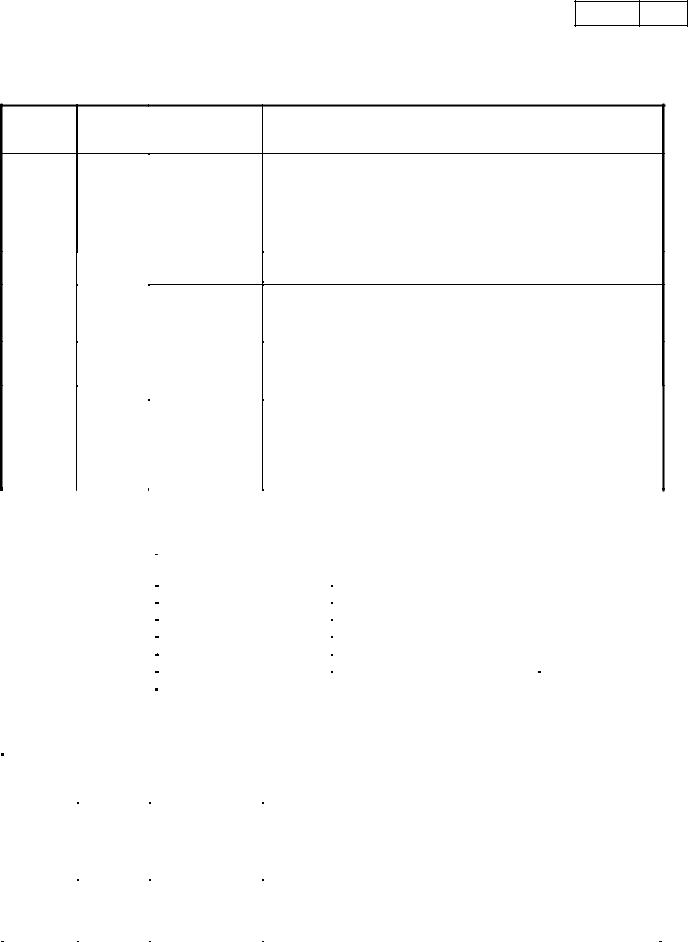
For U.S.A., Canada, Europe & Korea model
SERVICE MANUAL
MODEL DN-D4000
DOUBLE CD PLAYER
 Please use this service manual with referring to the operating instructions without fail.
 Some illustrations using in this service manual are slightly different from the actual set.
|

 8
8


16-11, YUSHIMA 3-CHOME, BUNKYOU-KU, TOKYO 113-0034 JAPAN
Telephone: 03 (3837) 5321
X0171V.01 DE/CDM 0303
DN-D4000 1
SAFETY PRECAUTIONS
The following check should be performed for the continued protection of the customer and service technician.
LEAKAGE CURRENT CHECK
Before returning the unit to the customer, make sure you make either (1) a leakage current check or (2) a line to chassis resistance check. If the leakage current exceeds 0.5 milliamps, or if the resistance from chassis to either side of the power cord is less than 460 kohms, the unit is defective.
LASER RADIATION
Do not stare into beam or view directly with optical instruments, class 3A laser product.
 500V
500V


 1M
1M


(1) 


(2) 


(1)

(2)

1
DN-D4000 2
DISASSEMBLY
(Follow the procedure below in reverse order when reassembling)
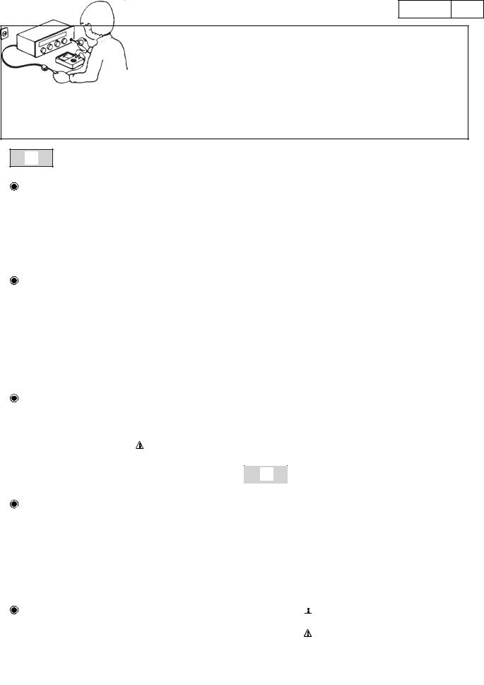
1.TOP COVER
(1)Remove 4 screws on the both sides, and 1 screw on rear side, then remove 1 upper screw.
(2)Pull up Top Cover.
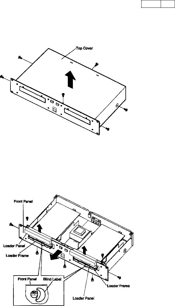
2.FRONT PANEL
(1)Detach 2 Blind Labels on the bottom chassis.
(2)Move CD Mecha Rack in the arrow direction through the label detached chassis opening. Loader Frame comes out.
(3)Pull up Loader Panel while pulling it towards front.
(4)Remove 2 upper screws and 3 lower screws, and 2 screws on both sides.
(5)Detach Front Panel.
2

DN-D4000 3
3.MECHANISM UNIT
(1)Disconnect FFC cable.
(2)Rrmove 8 lower screws
(3)Remove 4 screws on rear side.
NOTES:
(a)Do notpull out aslant to prevent the FFC cable from damage.
(b)Do not fail to pull out AC cord from wall outlet befor disconnecting the FFCcable. If the ACcord is remained plugged into wall outlet, the power is kept supplied in the unit, which may cause danger.
4.MAIN P.W.B.
(1)Remove 4 screws.
(2)Disconnect Connector.
(3)Detach Main P.W.B.
3
DN-D4000 4
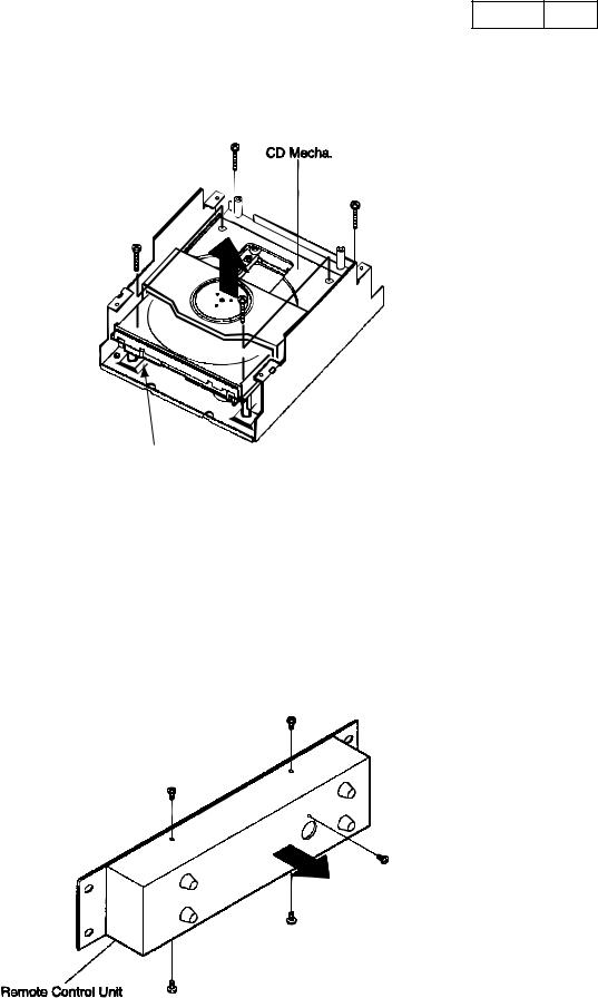
5.CD MECHA.
(1)A gear is turned and a tray is opened.
(2)Remove 4 upper screws.
(3)Detach CD Mecha.
Gear
6.COVER ( REMOTE CONTROL UNIT )
(1)Remove 5 screws.
NOTE:
(a)Remote Control Unit and its back panel are connected with cables, so pay attention when removing the back panel.
4

BLOCK DIAGRAM
<DN-D4000 DOUBLE CD
PLAYER>
LIMIT SW |
|
MAIN UNIT 1 |
|
|
|
|
|
|
|
||
SLIDE MOTOR |
M |
16M DRAM |
16M DRAM |
|
|
SPINDLE |
|
|
|||
M |
[M11L1644SA-50T] |
[M11L1644SA-50T] |
|
||
MOTOR |
IC204 |
IC210 |
|
||
|
|
||||
|
|
DRIVER |
|
|
|
|
|
[AN8785SB] |
|
|
|
LOADING MOTOR |
M |
IC202 |
PULSE |
|
|
DIGITAL SERVO PROCESSOR |
DIG OUT 1 |
||||
|
|
TRANS |
|||
CLOSE |
|
[MN6627911AC] |
|
||
SW |
|
IC201 |
|
|
|
OPEN SW |
|
|
|
|
|
|
|
|
+9VP |
|
FOCUS COIL |
|
|
|
[NJM78L05AT] |
|
|
TRACKING COIL |
|
|
|
|
||
|
|
|
IC118 |
|
||
|
|
|
|
|
|
|
MONITOR DIODE |
|
|
|
|
|
|
LASER DIODE |
|
HEAD AMP |
|
|
|
|
|
|
|
[AN22002A] |
[TC74HCT7007AF] |
[BU2618FV] |
VCO |
|
|
|
IC203 |
|||
|
|
|
[TC9246F] |
|||
|
|
|
|
IC112 |
IC113 |
|
|
|
|
|
IC114 |
||
DETECT |
E |
A B |
|
|
|
|
|
|
|
|
|||
OR |
|
D C |
F |
SYSTEM uCOM |
|
|
|
|
|
|
[MN102H60KDA] |
|
|
|
|
|
|
IC101 |
|
|
CD MECHA |
8M FLASH MEMORY |
DAC |
TR MUTE |
ANA OUT 1 |
UNIT 1 |
[PCM1748E] |
|||
[ M29W800DB70] |
IC206 |
|
|
|
|
IC111 |
|
|
|
LED1 |
|
|
|
FADER 1 |
UNIT |
|
|
|
|
POWER UNIT |
|
|
|
|
|
|
|
|
+9VP |
|
|
|
|
|
+5V REG |
+5VD |
|
|
|
|
|
+3.3V REG |
+3.3VD |
|
|
|
|
|
+1.8V REG |
+1.8V |
RESET |
,MBSY |
|
+9V,-HB,F1,F2 |
|
|
|
[PST600C] |
|
||
|
|
|
[SN74AHCT08PW] |
|
||
POWER |
+5V REG (AUDIO) |
+5VA |
IC301 |
RC TXD,RC RXD |
||
|
|
|
BSY |
IC302 |
|
|
TRANS |
-5V REG (AUDIO) |
-5VA |
|
|
8P MD |
|
|
|
|
|
|||
|
|
|
|
|
|
CABLE |
-HB REG |
-HB |
|
|
|
|
|
|
F2 |
|
|
|
|
|
AC |
F1 |
|
|
|
|
|
|
|
|
|
|
|
|
CD MECHA |
|
|
|
|
|
FADER 2 |
UNIT 2 |
|
|
|
|
|
|
|
|
|
|
|
|
|
|
|
|
MAIN UNIT 2 |
|
|
DIG OUT 2 |
LED2 |
|
|
|
|
|
|
|
|
|
|
|
ANA OUT 2 |
|
UNIT |
|
|
|
|
|
|
|
|
|
|
|
|
|
|
DN-D4000 |
6 |
|
<DN-D4000 REMOTE |
|
|
|
CONTROLLER> |
|
|
|
PANEL UNIT 1 |
|
|
FLT |
LED BLOCK |
KEY |
|
[14-MT-35GN] |
|
|
|
|
JOG SHUTTLE |
|
|
FL601 |
|
|
|
|
TR.SEL |
|
|
|
|
|
|
FL DRIVER |
LED CONTROL |
KEY MATRIX |
|
BLOCK |
|
||
[M66005FP] |
[BU2090F] |
|
|
|
|
||
IC601 |
IC602 |
|
|
PITCH |
|
|
|
SLIDE VR |
|
|
|
|
REMOTE CPU |
|
|
UNIT |
|
|
+9V |
|
|
[NJM7805FA(S)] |
|
|
IC404 |
|
|
RESET |
|
|
[PST600C] |
|
+9V,-HB,F1,F2 |
IC403 |
|
|
[SN74AHCT08PW] |
REMOTE uCOM |
|
[TMP86CM47U] |
|
|
IC302 |
|
|
IC402 |
|
|
|
|
|
PANEL |
|
|
UNIT 2 |
|
6
DN-D4000 7
SERVICE PROGRAM
Required Measuring Implement
1.Reference disc (TCD784 or CO-74176)
1.What is Service Program
Service program is a special program intended for confirming servo functions etc.
2. Contents of Service Program
Switch on the power while pushing the CD1’s PITCH BEND + button and CD2’s OPEN/CLOSE button at the same time. After actuating the servo program, select an aiming process number with the SELECT knob, A1 button, or A3 button. Press the SELECT knob to execute the selected process, the process number is then displayed on the track indicator of the display. To exit from the service program, just switch off the power.
|
|
Function |
Contents |
|
|
(Character-display) |
|
|
|
|
|
|
|
|
|
|
|
μcom Version check |
Check Version with JOG dial. |
|
|
1. System μcom version No.: “SysVerXXXX” |
|
|
|
(Version No.) |
|
|
|
2. RC μcom version No.: “RC_VerXXXX” |
|
|
|
|
|
|
|
|
|
|
|
|
|
Turn the JOG dial to display the logging error codes in the occurred order. |
|||
|
|
|
|
||||
|
|
|
|
“ErrXX_E * * * ” XX : occurred order E * * * : error code |
|||
|
|
|
Error Code Check |
10 error logs are memorized at maximum. |
|||
|
|
|
Kinds of Error Code, displayed |
||||
|
|
|
(Error Data) |
||||
|
|
|
|||||
|
|
|
Error Code Table |
||||
|
|
|
|
||||
|
|
|
|
Pressing SELECT knob enters to data erase mode. (“Err Clear?” is displayed.) |
|||
|
|
|
|
If the SELECT knob is pushed again, the memorized error data are cleared. |
|
|
|
|
|
|
|
|
|||
|
|
|
|
|
|
|
|
|
|
|
|
Total time span of servo function that counted by the hour is displayed. |
|
|
|
|
|
|
|
“R.Tim XXXXH” |
|
|
|
|
|
|
Total Running Time |
|
|
|
|
|
|
|
(Total_Time) |
Note: No time is counted if disc tray is opened within 59 minutes. |
|
|
|
|
SELECT knob |
|
|
Pressing SELECT knob enters to data erase mode. (“Time Clear?” is displayed.) |
|
|
|
|
|
|
If the SELECT knob is pushed again, the memorized time data are cleared. |
|
|
||
|
|
|
|
|
|
||
|
|
|
|
|
|
|
|
|
|
|
|
Starts automatic servo adjustment when the SELECT knob is pushed, and after |
|
|
|
|
|
|
|
completing the adjustment, sort of the used disc is indicated. Data is selectable with |
|||
|
|
|
|
the JOG dial. “Servo_Data” |
|||
|
|
|
|
1. |
Focus gain data |
||
|
|
|
|
2. |
Focus balance data |
||
|
|
|
Automatic |
3. |
Focus offset data |
||
|
|
|
Servo Adjustment |
4. |
Tracking gain data |
|
|
|
|
||||||
|
|
|
call |
5. |
Tracking balance data |
|
|
|
|
|
|
6. |
Tracking offset data |
|
|
|
|
|
|
|
|
|
|
7
DN-D4000 8
Function
Contents
(Character-display)
Loading a disc by OPEN/CLOSE button.
Block Error Rate Check Press the PLAY/PAUSE button. B.E.R. is displayed.
“E.Rate_XXX XXX : Block Error Rate
You can select the track by the JOG DIAL.
|
|
|
Starts automatic servo checking when the SELECT knob is pushed. |
|
|
|
|
||
|
|
|
Loading a disc by OPEN/CLOSE button. |
|
SELECT knob |
Servo Check |
“Lchk_Open” |
: Disc Tray is opened. |
|
|
|
|
“Lchk_Wait” |
: During check. |
|
|
|
||
|
|
|
“Lchk_OK!!” |
: Disc Tray is opened. |
|
|
|
“LchkErr *** ” : Error(E ***) is occurred. |
|
|
|
|
|
|
|
|
|
|
|
|
|
|
All illuminations are lit. |
|
|
Illumination Check |
All illuminations can be turned off to push the SELECT knob. |
||
|
|
|
Press the SELECT knob again, all illuminations can be lit. |
|
|
|
|
|
|
|
|
|
Adjustment Item |
|
Adjustment Value indication at |
|
||
|
|
|
|
character portions. |
|
|||
|
|
|
|
|
|
|
||
|
|
|
Focus Gain |
|
|
0576 ~ 2304 |
|
|
|
|
|
Focus Balance |
|
|
-050 ~ +050 |
|
|
|
|
|
Focus Offset |
|
|
-005 ~ +005 |
|
|
|
|
|
Tracking Gain |
|
|
0392 ~ 1569 |
|
|
|
|
|
Tracking Balance |
|
|
-025 ~ +025 |
|
|
|
|
|
Tracking Offset |
|
|
-005 ~ +005 |
|
|
|
|
|
* Reference data. |
|
|
|||
3. TEST MODE |
|
|
|
|
|
|
||
|
|
|
|
|
|
|
|
|
|
Process No. |
|
Function |
|
|
|
|
|
|
(TRACK |
|
|
|
Contents |
|||
|
|
(Character-display) |
|
|
||||
|
Indication) |
|
|
|
|
|
||
|
|
|
|
|
|
|
||
|
|
|
|
|
||||
|
|
|
|
Starting with the PLAY/PAUSE button, it repeats open/close of the tray and |
||||
|
|
Heat Run |
playback. |
|
|
|||
A1 button |
- |
All tracks are played back if the track count is less than 20. Only the first and last |
||||||
(H/R1Normal) |
||||||||
|
|
tracks are played back if the tracks are more than 21. When any errors, it stops |
||||||
|
|
|
|
|||||
|
|
|
|
and indicates error code (see Error Code Table). |
||||
|
|
|
|
|
||||
|
|
|
|
Starting with the PLAY/PAUSE button, it repeats open/close of the tray, servo on, |
||||
A2 button |
- |
Chucking Test |
and TOC read. |
|
|
|||
(H/R2_Tray) |
The display shows the number of the tray operation. When any errors, it stops and |
|||||||
|
|
|||||||
|
|
|
|
indicates error code (see Error Code Table ). |
||||
|
|
|
|
|
|
|
|
|
8

DN-D4000 9
4. Error Code Table
Error Code |
CONTENTS |
|
|
E001 |
Unable to close the loader tray in the regulation time. |
|
|
E002 |
Unable to open the loader tray in the regulation time. |
|
|
E003 |
Inner circle switch ON error even if the time is over. |
|
|
E004 |
Inner circle switch OFF error even if the time is over. |
|
|
E005 |
The focus offset adjustment result is outside the regulation range. |
|
|
E006 |
Unable to adjust the focus offset in the regulation time. |
|
|
E007 |
The tracking offset adjustment result is outside the regulation range. |
|
|
E008 |
Unable to adjust the tracking offset in the regulation time. |
|
|
E009 |
The FE peak is outside the regulation range. |
|
|
E00A |
The FE peak is outside the regulation range. |
|
|
E00B |
Unable to adjust the focus rough gain in the regulation time. |
|
|
E00C |
The focus rough gain is outside the regulation range. |
|
|
E00D |
Unable to actuate focus in the regulation time. |
|
|
E00E |
Unable to actuate tracking in the regulation time. |
|
|
E00F |
Unable to adjust the tracking rough gain in the regulation time. |
|
|
E010 |
The tracking rough gain is outside the regulation range. |
|
|
E011 |
Unable to adjust the tracking balance in the regulation time. |
|
|
E012 |
The tracking balance adjustment result is outside the regulation range. |
|
|
E013 |
Focus servo down during automatic adjustment. |
|
|
E014 |
Focus servo down during automatic adjustment. |
|
|
E015 |
Unable to adjust the focus balance in the regulation time. |
|
|
E016 |
The focus balance adjustment result is outside the regulation range. |
|
|
E017 |
Track servo down during automatic adjustment. |
|
|
E018 |
Unable to adjust the focus fine gain in the regulation time. |
|
|
E019 |
The focus fine gain is outside the regulation range. |
|
|
E01A |
Unable to adjust the tracking fine gain in the regulation time. |
|
|
E01B |
The tracking fine gain is outside the regulation range. |
|
|
E01C |
Unable to adjust automatically in the regulation time. |
|
|
E01D |
Unable to read the subcode Q in the regulation time. |
|
|
E01E |
Unable to read the TOC in the regulation time. |
|
|
E01F |
Focus servo down during search (over the regulation time). |
|
|
E020 |
Track servo down during search (over the regulation time). |
|
|
E0216 * |
Servo error during search. |
|
|
E0213 * |
Search error (over the regulation time). |
|
|
E022 |
Discontinuity occurred, during write to the DRAM. |
|
|
E023 |
The error which cannot be corrected to the read data. |
|
|
E024 |
Unable to do the level detect. |
|
|
E025 |
Unable to join data in the regulation time. |
|
|
E026 |
The error rate when recording on the memory is over the regulation value. |
|
|
E027 |
The subcode jump more than regulation. |
E028 |
Servo error when power is turned on. |
|
|
E029 |
Subcode Q error. |
|
|
E030 |
Inter face error for both drives. |
|
|
9
DN-D4000 10
μCOM VERSION UPGRADE
System µcom can be upgraded in the following manner.
Version Upgrade Method
1.Record the version upgrade software on a CD-R or CD-RW disc, only as one file with the format ISO9660 Mode-1.
The file name of the supplied version upgrade software should be used as is and this disc needs to finalize.
2.Hold the disc by the edges and place it on the disc tray. 3.Press the OPEN/CLOSE button to start the version upgrade.
"Version Up"→"Push Play!" "xxxx->XXXX" are displayed. xxxx : current version XXXX : upgrade version
4.Press the PLAY/PAUSE button.
"Now Writing" → "Writing-XXX" are displayed.
XXX : count up from 000 to161 5.When the version upgrade is finished, "Complete!" is indicated. 6.Turn off the power once and turn on again.
Press the OPEN/CLOSE button and remove the disc.
NOTE: When the power is turned off before "Complete!" is displayed, µcom version is not written correctly.
10
DN-D4000 11
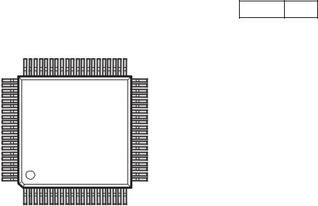
SEMICONDUCTORS
 IC’s
IC’s
MN102H60KDA
(IC101)
75 |
51 |
76 |
50 |
100 |
26 |
1 |
25 |
MN102H60KDA Terminal Function
Pin |
Pin Name |
Symbol |
I/O |
DET |
Ext |
Res |
Ini |
Function |
|
No. |
|
||||||||
|
|
|
|
|
|
|
|
|
|
|
|
|
|
|
|
|
|
|
|
1 |
P60, WAIT, SBT2 |
PCDMUTE |
O |
- |
Pd |
L |
L |
Mute for analog |
'L': Mute ON |
2 |
P61, _RE |
RD- |
O |
- |
Pu |
H |
- |
Read signal |
|
3 |
P62, _WEL |
WR- |
O |
- |
Pu |
H |
- |
Write signal |
|
4 |
P63, _WE, _WEH |
Reserved |
O |
- |
- |
Hi-Z |
L |
Not used. |
|
5 |
_CS0,TM13OA |
FLASHROMCS- |
O |
- |
Pu |
H |
- |
Chip select signal |
|
|
|
|
|
|
|
|
|
(MASK ROM operation : Input port) |
|
|
|
|
|
|
|
|
|
|
|
6 |
_CS1, TM13OB |
Reserved |
O |
- |
- |
Hi-Z |
L |
Not used. |
|
7 |
_CS2, TM14OA |
Reserved |
O |
- |
- |
Hi-Z |
L |
Not used. |
|
8 |
_CS3, TM14OB |
PLOAD |
O |
- |
- |
Hi-Z |
H |
OPEN/CLOSE signal (PWM out put) |
|
|
|
|
|
|
|
|
|
(During Pnrst= |
|
|
|
|
|
|
|
|
|
'L', out put PWM(50%)) |
|
|
|
|
|
|
|
|
|
|
|
9 |
P54, _BREQ |
Reserved |
O |
- |
- |
Hi-Z |
L |
Not used. |
|
10 |
P55, _BRACK |
Reserved |
O |
- |
- |
Hi-Z |
L |
Not used. |
|
11 |
P56, ALE, _ALE, |
MON2 |
I |
- |
- |
Hi-Z |
- |
Monitor signal 2 |
|
|
_BSTRE, TM15IA |
|
|
|
|
|
|
|
|
|
|
|
|
|
|
|
|
|
|
12 |
P57,_WORD |
WORD- |
I |
- |
L |
L |
- |
Data bit bus width select 'L': 16bit |
|
13 |
P20,A00,SBT2 |
A00 |
A/O |
- |
- |
Unfix |
- |
Address bus |
|
14 |
P21,A01,SBI2 |
A01 |
A/O |
- |
- |
Unfix |
- |
Address bus |
|
15 |
P22,A02,SBO2 |
A02 |
A/O |
- |
- |
Unfix |
- |
Address bus |
|
16 |
P23,A03 |
A03 |
A/O |
- |
- |
Unfix |
- |
Address bus |
|
17 |
Vdd |
Vdd |
- |
- |
- |
- |
- |
Power supply(+3.3V) |
|
18 |
BOSC,BIBT1,BIBT2, |
Reserved |
O |
- |
- |
L |
L |
Not used. |
|
|
PB0 |
|
|
|
|
|
|
|
|
|
|
|
|
|
|
|
|
|
|
19 |
Vss |
Vss |
- |
- |
- |
- |
- |
GND(0V) |
|
20 |
XI,PB1 |
PCE |
O |
- |
Pd |
L |
L |
Latch output |
|
21 |
XO |
XO |
- |
- |
- |
- |
- |
Not used. OPEN |
|
22 |
Vdd |
Vdd |
- |
- |
- |
- |
- |
Power supply(+3.3V) |
|
23 |
OSCI |
OSCI |
I |
- |
- |
- |
- |
Not used. |
|
24 |
OSCO |
OSCO |
O |
- |
- |
- |
- |
OSCI output |
|
25 |
MODE |
MODE |
I |
- |
L |
L |
- |
Mode select 'L': Processor mode |
|
11

DN-D4000 12
Pin |
Pin Name |
Symbol |
I/O |
DET |
Ext |
Res |
Ini |
Function |
|
|
No. |
|
|
||||||||
|
|
|
|
|
|
|
|
|
|
|
|
|
|
|
|
|
|
|
|
|
|
26 |
P24,A04,TM15IA |
A04 |
A/O |
- |
- |
Unfix |
- |
Address bus |
|
|
27 |
P25,A05 |
A05 |
A/O |
- |
- |
Unfix |
- |
Address bus |
|
|
28 |
P26,A06 |
A06 |
A/O |
- |
- |
Unfix |
- |
Address bus |
|
|
29 |
P27,A07 |
A07 |
A/O |
- |
- |
Unfix |
- |
Address bus |
|
|
30 |
P30,A08,_KI0 |
A08 |
A/O |
- |
- |
Unfix |
- |
Address bus |
|
|
31 |
P31,A09,_KI1 |
A09 |
A/O |
- |
- |
Unfix |
- |
Address bus |
|
|
32 |
P32,A10,_KI2 |
A10 |
A/O |
- |
- |
Unfix |
- |
Address bus |
|
|
33 |
P33,A11,_KI3 |
A11 |
A/O |
- |
- |
Unfix |
- |
Address bus |
|
|
34 |
AVDD |
AVDD |
- |
- |
- |
- |
- |
Analog power supply terminal |
||
35 |
P34,A12,_KI4 |
A12 |
A/O |
- |
- |
Unfix |
- |
Address bus |
|
|
36 |
P35,A13,_KI5 |
A13 |
A/O |
- |
- |
Unfix |
- |
Address bus |
|
|
37 |
P36,A14,_KI6 |
A14 |
A/O |
- |
- |
Unfix |
- |
Address bus |
|
|
38 |
P37,A15,_KI7 |
A15 |
A/O |
- |
- |
Unfix |
- |
Address bus |
|
|
39 |
P40,A16 |
A16 |
A/O |
- |
- |
Unfix |
- |
Address bus |
|
|
40 |
P41,A17 |
A17 |
A/O |
- |
- |
Unfix |
- |
Address bus |
|
|
41 |
P42,A18 |
A18 |
A/O |
- |
- |
Unfix |
- |
Address bus |
|
|
42 |
P43,A19 |
A19 |
A/O |
- |
- |
Unfix |
- |
Address bus |
|
|
43 |
Vref- |
Vref- |
- |
- |
- |
- |
- |
Standard analog power supply |
||
44 |
P44,AN4,A20 |
POPEN |
I |
- |
- |
Unfix |
- |
OPEN switch |
'L': Switch ON |
|
45 |
P45,AN5,A21 |
PCLOSE |
I |
- |
- |
Unfix |
- |
CLOSE switch |
'L': Switch ON |
|
46 |
P46,AN6,STOP,A22 |
PLIMITSW |
I |
- |
- |
Hi-Z |
- |
Inner circle SW |
'L': Switch ON |
|
47 |
P47,AN7,WDOUT, |
PCDSEL |
I |
- |
H/L |
H/L |
- |
CD mecha select switch |
||
|
A23 |
|
|
|
|
|
|
'L': Mecha 1 / 'H': Mecha 2 |
||
|
|
|
|
|
|
|
|
|
|
|
48 |
P80,TM14OA |
PEJECTSW |
I |
- |
Pu |
H |
- |
Eject switch |
'L': Switch ON |
|
49 |
P81,TM14OB |
PTLED |
O |
- |
Pd |
L |
L |
Toray LED |
'H': Light 1 / 'L': Turn Off |
|
50 |
P82,TM0IO,SBI2, |
PDMUTE |
O |
- |
Pu |
H |
H |
Mute for digital |
'H': Mute ON |
|
|
SBT3,SCL3 |
|
|
|
|
|
|
|
|
|
|
|
|
|
|
|
|
|
|
||
51 |
P83,TM4IO,SBI3 |
RxD |
I |
- |
Pu |
H |
- |
Serial port (Receive) |
||
|
|
|
|
|
|
|
|
(76.8kbps |
5V -> 3.3V) |
|
52 |
P84,TM7IO,SBO3, |
TxD |
O |
- |
Pu |
H |
H |
Serial port (Transmission) |
||
|
SDA3 |
|
|
|
|
|
|
(76.8kbps , Use ATC function) |
||
|
|
|
|
|
|
|
|
|
||
53 |
P85,TM9IOA,SBO2, |
PMD |
O |
- |
Pu |
L |
L |
DAC(PCM1748) control signal : Data |
||
|
SBT4,SCL4 |
|
|
|
|
|
|
|
|
|
|
|
|
|
|
|
|
|
|
||
54 |
Vref+ |
Vref+ |
- |
- |
- |
- |
- |
Standard analog power supply |
||
55 |
P86,TM9IOB,SBI4 |
PMECHRxD |
I |
- |
- |
Hi-Z |
- |
Serial port (Receive) |
||
56 |
P87,TM9IC,SBO4, |
PMECHTxD |
O |
- |
- |
Hi-Z |
H |
Serial port (Transmission) |
||
|
SDA4 |
|
|
|
|
|
|
(76.8kbps , Use ATC function) |
||
|
|
|
|
|
|
|
|
|
|
|
57 |
P90,TM8IOA,BIBT1, |
PMC |
O |
- |
Pd |
L |
L |
DAC(PCM1748) |
|
|
|
_DMAREQ1 |
|
|
|
|
|
|
control signal : Clock |
||
58 |
P91,TM10IOA, |
PML |
O |
- |
Pd |
L |
L |
DAC(PCM1748) |
|
|
|
BIBT2,_DMAACK1 |
|
|
|
|
|
|
control signal : Latch |
||
|
|
|
|
|
|
|
|
|
||
59 |
P92,TM10IOB, |
PLRCK |
I |
Ed |
- |
Hi-Z |
- |
LRCK : Use for time code creation |
||
|
_DMAREQ0 |
|
|
|
|
|
|
during MP3 playback. |
||
|
|
|
|
|
|
|
|
|
||
60 |
P93,TM10IC, |
PNRST |
O |
- |
Pd |
L |
L |
Round IC reset signal |
||
|
_DMAACK0 |
|
|
|
|
|
|
|
|
|
61 |
Vss |
Vss |
- |
- |
- |
- |
- |
GND(0V) |
|
|
62 |
P94,AN0 |
PMBSYOUT |
O |
- |
- |
Hi-Z |
H |
Mechanism microcomputer |
||
|
|
|
|
|
|
|
|
Communication Busy signal output |
||
|
|
|
|
|
|
|
|
'H':BUSY |
|
|
|
|
|
|
|
|
|
|
|
||
63 |
P95,AN1 |
PMBSYIN |
I |
- |
- |
Hi-Z |
- |
Mechanism microcomputer |
||
|
|
|
|
|
|
|
|
Communication Busy signal input |
||
64 |
P96,AN2 |
PRCBSYOUT |
O |
- |
- |
Hi-Z |
H |
Communication Busy signal output |
||
|
|
|
|
|
|
|
|
between RC and Mecha 'H':BUSY |
||
12
|
|
|
|
|
|
|
|
|
DN-D4000 |
13 |
|
|
|
|
|
|
|
|
|
|
|
|
|
|
|
|
|
|
|
|
|
|
|
|
|
Pin |
Pin Name |
Symbol |
I/O |
DET |
Ext |
Res |
Ini |
Function |
|
||
No. |
|
||||||||||
|
|
|
|
|
|
|
|
|
|
||
|
|
|
|
|
|
|
|
|
|
||
65 |
P97,AN3 |
PRCBSYIN |
I |
- |
- |
Hi-Z |
- |
Communication Busy signal input |
|
||
|
|
|
|
|
|
|
|
between RC and Mecha |
|
||
|
|
|
|
|
|
|
|
|
|
||
66 |
Vdd |
Vdd |
- |
- |
- |
- |
- |
Power supply(+3.3V) |
|
||
67 |
P70,SBT0,_RAS |
PMCLK |
O |
- |
- |
Hi-Z |
H |
DSP interface Clock |
|
||
|
|
|
|
|
|
|
|
(clock synchronous formula) |
|
||
|
|
|
|
|
|
|
|
|
|
||
68 |
P71,SBI0,_CAS,_LC |
PSTAT |
I |
- |
- |
Hi-Z |
- |
DSP interface Reception |
|
||
|
AS |
|
|
|
|
|
|
(clock synchronous formula) |
|
||
|
|
|
|
|
|
|
|
|
|
||
69 |
P72,SBO0,_UCAS |
PMDAT |
O |
- |
- |
Hi-Z |
H |
DSP interface Transmission |
|
||
|
|
|
|
|
|
|
|
(clock synchronous formula) |
|
||
70 |
P73,SBT1,DUMX |
PTXTCLK |
O |
- |
- |
Hi-Z |
H |
Use during CD-TEXT data read |
|
||
|
|
|
|
|
|
|
|
(clock synchronous formula) |
|
||
|
|
|
|
|
|
|
|
|
|
||
71 |
P74,SBI1 |
PTXTD |
I |
- |
- |
Hi-Z |
- |
Use during CD-TEXT data read |
|
||
|
|
|
|
|
|
|
|
(clock synchronous formula) |
|
||
|
|
|
|
|
|
|
|
|
|
||
72 |
P75,SBO1 |
PMLD |
O |
- |
- |
Hi-Z |
H |
DSP interface latch |
|
||
73 |
TEST1 |
TEST1 |
I |
- |
Pu |
- |
- |
Pull up 33 - 50K |
|
||
74 |
TEST2 |
TEST2 |
I |
- |
Pu |
- |
- |
Pull up 33 - 50K |
|
||
75 |
_NMI |
_NMI |
I |
Lv |
Pu |
H |
- |
Need to pull up |
|
||
76 |
PA0,_IRQ0 |
PBLKCK |
I |
Ed |
- |
Hi-Z |
- |
Sub code clock interruption |
|
||
77 |
PA1,_IRQ1 |
PDQSY |
I |
Ed |
- |
Hi-Z |
- |
CD-TEXT DQSY Interruption |
|
||
78 |
PA2,_IRQ2 |
PFADECUE |
I |
- |
Pu |
H |
- |
Fader signal input (CUE) |
|
||
|
|
|
|
|
|
|
|
'L' : Input YES |
|
||
79 |
PA3,_IRQ3 |
PFADER ST |
I |
- |
Pu |
H |
- |
Fader signal input (PLAY) |
|
||
|
|
|
|
|
|
|
|
'L' : Input YES |
|
||
|
|
|
|
|
|
|
|
|
|
||
80 |
PA4,_IRQ4,TM15IB |
PCHGOFT |
O |
- |
Pu |
H |
L |
Off track signal |
|
||
81 |
PA5,ADSEP |
ADSEP |
I |
- |
H |
H |
H |
H': Address data separation mode / |
|
||
|
|
|
|
|
|
|
|
'L': Address data common mode |
|
||
82 |
_RST |
RST- |
I |
Lv |
- |
L |
- |
Reset signal 'L': RESET |
|
||
83 |
Vdd |
Vdd |
- |
- |
- |
- |
- |
Power supply(+3.3V) |
|
||
84 |
P00,D00,AD00 |
D00 |
D/O |
- |
- |
Hi-Z |
- |
Data bus |
|
||
85 |
P01,D01,AD01 |
D01 |
D/O |
- |
- |
Hi-Z |
- |
Data bus |
|
||
86 |
P02,D02,AD02 |
D02 |
D/O |
- |
- |
Hi-Z |
- |
Data bus |
|
||
87 |
P03,D03,AD03 |
D03 |
D/O |
- |
- |
Hi-Z |
- |
Data bus |
|
||
88 |
P04,D04,AD04 |
D04 |
D/O |
- |
- |
Hi-Z |
- |
Data bus |
|
||
89 |
P05,D05,AD05 |
D05 |
D/O |
- |
- |
Hi-Z |
- |
Data bus |
|
||
90 |
P06,D06,AD06 |
D06 |
D/O |
- |
- |
Hi-Z |
- |
Data bus |
|
||
91 |
P07,D07,AD07 |
D07 |
D/O |
- |
- |
Hi-Z |
- |
Data bus |
|
||
92 |
Vss |
Vss |
- |
- |
- |
- |
- |
GND(0V) |
|
||
93 |
P010,D08,AD08,TM |
D08 |
D/O |
- |
- |
Hi-Z |
- |
Data bus |
|
||
|
8IOB |
|
|
|
|
|
|
|
|
|
|
94 |
P011,D09,AD09,TM |
D09 |
D/O |
- |
- |
Hi-Z |
- |
Data bus |
|
||
|
8IC |
|
|
|
|
|
|
|
|
|
|
|
|
|
|
|
|
|
|
|
|
||
95 |
P012,D10,AD10,TM |
D10 |
D/O |
- |
- |
Hi-Z |
- |
Data bus |
|
||
|
11IOA |
|
|
|
|
|
|
|
|
|
|
|
|
|
|
|
|
|
|
|
|
||
96 |
P013,D11,AD11,TM |
D11 |
D/O |
- |
- |
Hi-Z |
- |
Data bus |
|
||
|
11IOB |
|
|
|
|
|
|
|
|
|
|
97 |
P014,D12,AD12,TM |
D12 |
D/O |
- |
- |
Hi-Z |
- |
Data bus |
|
||
|
11IC |
|
|
|
|
|
|
|
|
|
|
|
|
|
|
|
|
|
|
|
|
||
98 |
P015,D13,AD13,TM |
D13 |
D/O |
- |
- |
Hi-Z |
- |
Data bus |
|
||
|
12IOA |
|
|
|
|
|
|
|
|
|
|
|
|
|
|
|
|
|
|
|
|
||
99 |
P016,D14,AD14,TM |
D14 |
D/O |
- |
- |
Hi-Z |
- |
Data bus |
|
||
|
12IOB |
|
|
|
|
|
|
|
|
|
|
100 |
P017,D15,AD15,TM |
D15 |
D/O |
- |
- |
Hi-Z |
- |
Data bus |
|
||
|
12IC |
|
|
|
|
|
|
|
|
|
|
13
DN-D4000 14
MN6627911AC
(IC201)
60 |
41 |
61 |
40 |
80 |
21 |
1 |
20 |
MN6627911AC Terminal Function
Pin No. |
Pin Name |
I/O |
|
Function |
|
|
|
|
|
|
|
|
|
|
1 |
DRVDD |
I |
Power supply for DRAM interface (Pin No.2 - 18, 80) |
|
2 |
D0 |
I/O |
Data I/O signal 0 for DRAM |
|
3 |
D1 |
I/O |
Data I/O signal 1 for DRAM |
|
4 |
WE |
O |
Write enable signal for DRAM |
|
|
|
|
|
|
5 |
RAS |
O |
RAS control signal for DRAM |
|
6 |
D2 |
I/O |
Data I/O signal 2 for DRAM |
|
7 |
D3 |
I/O |
Data I/O signal 3 for DRAM |
|
|
|
|
|
|
8 |
CAS |
O |
CAS control signal 0 for DRAM |
|
9 |
A10 |
O |
Address signal 10 for DRAM |
|
10 |
A8 |
O |
Address signal 8 for DRAM |
|
|
|
|
|
|
11 |
A7 |
O |
Address signal 7 for DRAM |
|
12 |
A6 |
O |
Address signal 6 for DRAM |
|
13 |
A5 |
O |
Address signal 5 for DRAM |
|
|
|
|
|
|
14 |
A4 |
O |
Address signal 4 for DRAM |
|
15 |
A9 |
O |
Address signal 9 for DRAM |
|
16 |
A0 |
O |
Address signal 0 for DRAM |
|
|
|
|
|
|
17 |
A1 |
O |
Address signal 1 for DRAM |
|
18 |
A2 |
O |
Address signal 2 for DRAM |
|
19 |
A3 |
O |
Address signal 3 for DRAM |
|
|
|
|
|
|
20 |
DVSS2 |
I |
GND for digital |
|
21 |
DVDD2 |
I |
Power supply for digital |
|
22 |
SPOUT |
O |
Spindle motor drive signal |
|
|
|
|
|
|
23 |
TRVP |
O |
Traverse drive signal |
|
24 |
TRVM |
O |
Not used |
|
|
|
|
|
|
25 |
TRP |
O |
Tracking drive |
|
|
|
|
|
|
26 |
GCNTL |
O |
Gain control signal for CD-RW |
|
27 |
FOP |
O |
Focus drive |
|
|
|
|
|
|
28 |
CHGICO |
O |
EQ select signal |
|
|
|
|
|
|
29 |
IOVDD1 |
I |
Power supply for IO |
|
30 |
TBAL |
O |
Tracking balance adjust |
|
|
|
|
|
|
31 |
FBAL |
O |
Focus balance adjust |
|
|
|
|
|
|
32 |
FE |
I |
Focus error signal (Analog input) |
|
33 |
TE |
I |
Tracking error signal (Analog input) |
|
|
|
|
|
|
34 |
RFENV |
I |
RF envelope signal (Analog input) |
|
|
|
|
|
|
35 |
OFT |
I |
Off track signal |
H : OFF TRACK |
36 |
NRFDET |
I |
RF detect signal |
H : DETECT |
|
|
|
|
|
37 |
BDO |
I |
Drop out signal |
H : DROP OUT |
|
|
|
|
|
38 |
LDON |
O |
Laser ON signal |
H : ON |
39 |
ARF |
I |
RF signal |
|
|
|
|
|
|
40 |
IREF |
I |
Standard current input terminal |
|
|
|
|
|
|
41 |
ADPVCC |
I |
Voltage for power supply monitor |
|
14
DN-D4000 15
Pin No. |
Pin Name |
I/O |
|
|
|
Function |
|
|
|
|
|
|
|
|
|
|
|
|
|
|
42 |
DSLF |
O |
Loop filter for DSL |
|
|
|
43 |
RFSW |
I |
Loop filter for DSL |
|
|
|
|
|
|
|
|
|
|
44 |
PLLF |
O |
Loop filter for PLL |
|
|
|
45 |
PLLFO |
O |
Loop filter for PLL |
|
|
|
46 |
AVDD2 |
I |
Power supply for analog (DSL, PLL, AD) |
|||
|
|
|
|
|||
47 |
AVSS2 |
I |
GND for analog (DSL, PLL, AD) |
|||
48 |
OUTL |
O |
Not used |
|
|
|
49 |
AVSS1 |
I |
GND for analog (Audio output) |
|
||
|
|
|
|
|
|
|
50 |
OUTR |
O |
Not used |
|
|
|
51 |
AVDD1 |
I |
Power supply for analog (Audio output) |
|||
52 |
DVSS3 |
I |
GND for digital |
|
|
|
|
|
|
|
|
||
53 |
DVDD3 |
I |
Power supply for digital |
|
||
54 |
TMOD2 |
I |
Test terminal |
L : Normal |
|
|
55 |
MON2 |
O |
Serial monitor signal 2 |
|
||
|
|
|
|
|
||
56 |
BCLK |
O |
Bit clock for serial data |
|
||
57 |
SRDATA |
O |
Serial data signal |
|
|
|
58 |
LRCK |
O |
L, R discernment signal |
|
||
|
|
|
|
|
||
59 |
IOVDD2 |
I |
Power supply for IO |
|
||
60 |
TX |
O |
Digital audio interface signal |
|
||
61 |
MCLK |
I |
ucon command clock signal |
|
||
|
|
|
|
|
||
62 |
MDATA |
I |
ucon command data signal |
|
||
63 |
MLD |
I |
ucon command load signal |
L : LOAD |
||
64 |
BLKCK |
O |
Sub code block clock signal (f=75Hz : Normal speed playback) |
|||
|
|
|
|
|
||
65 |
PWMSEL |
I |
PWM output mode select |
L : Direct H : 3 values |
||
66 |
SMCK |
O |
Not used |
|
|
|
67 |
SBCK |
I |
Not used |
|
|
|
|
|
|
|
|
|
|
68 |
STAT |
O |
Status signal |
|
|
|
69 |
NRST |
I |
Reset |
L : RESET |
|
|
70 |
SPPOL |
O |
Not used |
|
|
|
|
|
|
|
|
|
|
71 |
PMCK |
O |
Not used |
|
|
|
72 |
DQSY |
O |
Pack signal for CD TEXT data |
|
||
73 |
TXTD |
O |
CD TEXT data signal |
|
||
|
|
|
|
|||
74 |
TXTCK |
O |
Ext. clock signal input for CD TEXT resister |
|||
75 |
NTEST |
I |
Test terminal |
H : Normal |
|
|
76 |
X2 |
O |
Not used |
|
|
|
|
|
|
|
|
||
77 |
X1 |
I |
16.9344MHz input terminal |
|
||
78 |
DVSS1 |
I |
GND for digital |
|
|
|
79 |
DVDD1 |
I |
Power supply for digital |
|
||
|
|
|
|
|
||
80 |
MON1 |
O |
Serial monitor signal |
|
||
15
 Loading...