


DN-X1700
Table of contents
 Loading...
Copyright 2010 D&M Holdings Inc. All rights reserved.
WARNING: Violators will be prosecuted to the maximum extent possible.
SERVICE MANUAL
DJ MIXER
MODEL JP E3 E2 EK E2A E2C E1K EUT
DN-X1700
33
Ver. 2
●
For purposes of improvement, specifications and design are subject to change without notice.
●
Please use this service manual with referring to the operating instructions without fail.
●
Some illustrations using in this service manual are slightly different from the actual set.
S0166-1V02DM/DG1010
Please refer to the
MODIFICATION NOTICE.
2
DN-X1700
Please heed the points listed below during servicing and inspection.
◎ Heed the cautions!
Spots requiring particular attention when servicing, such
as the cabinet, parts, chassis, etc., have cautions indicated
on labels or seals. Be sure to heed these cautions and the
cautions indicated in the handling instructions.
◎ Caution concerning electric shock!
(1) An AC voltage is impressed on this set, so touching in-
ternal metal parts when the set is energized could
cause electric shock. Take care to avoid electric shock,
by for example using an isolating transformer and
gloves when servicing while the set is energized, un-
plugging the power cord when replacing parts, etc.
(2)There are high voltage parts inside. Handle with extra
care when the set is energized.
◎ Caution concerning disassembly and
assembly!
Though great care is taken when manufacturing parts from
sheet metal, there may in some rare cases be burrs on the
edges of parts which could cause injury if fingers are
moved across them. Use gloves to protect your hands.
◎ Only use designated parts!
The set's parts have specific safety properties (fire resis-
tance, voltage resistance, etc.). For replacement parts, be
sure to use parts which have the same properties. In par-
ticular, for the important safety parts that are marked z on
wiring diagrams and parts lists, be sure to use the desig-
nated parts.
◎ Be sure to mount parts and arrange
the wires as they were originally!
For safety reasons, some parts use tape, tubes or other in-
sulating materials, and some parts are mounted away from
the surface of printed circuit boards. Care is also taken with
the positions of the wires inside and clamps are used to
keep wires away from heating and high voltage parts, so
be sure to set everything back as it was originally.
◎ Inspect for safety after servicing!
Check that all screws, parts and wires removed or discon-
nected for servicing have been put back in their original po-
sitions, inspect that no parts around the area that has been
serviced have been negatively affected, conduct an insu-
lation check on the external metal connectors and between
the blades of the power plug, and otherwise check that
safety is ensured.
(Insulation check procedure)
Unplug the power cord from the power outlet, disconnect
the antenna, plugs, etc., and turn the power switch on. Us-
ing a 500V insulation resistance tester, check that the in-
sulation resistance between the terminals of the power
plug and the externally exposed metal parts (antenna ter-
minal, headphones terminal, microphone terminal, input
terminal, etc.) is 1MΩ or greater. If it is less, the set must
be inspected and repaired.
Concerning important safety
parts
Many of the electric and structural parts used in the set
have special safety properties. In most cases these prop-
erties are difficult to distinguish by sight, and using re-
placement parts with higher ratings (rated power and
withstand voltage) does not necessarily guarantee that
safety performance will be preserved. Parts with safety
properties are indicated as shown below on the wiring dia-
grams and parts lists is this service manual. Be sure to re-
place them with parts with the designated part number.
(1) Schematic diagrams ... Indicated by the z mark.
(2) Parts lists ... Indicated by the z mark.
Using parts other than the designated
parts could result in electric shock, fires or
other dangerous situations.
SAFETY PRECAUTIONS
The following check should be performed for the continued protection of the customer and service technician.
LEAKAGE CURRENT CHECK
Before returning the unit to the customer, make sure you make either (1) a leakage current check or (2) a line to chassis
resistance check. If the leakage current exceeds 0.5 milliamps, or if the resistance from chassis to either side of the
power cord is less than 460 kohms, the unit is defective.
CAUTION
CAUTION
3
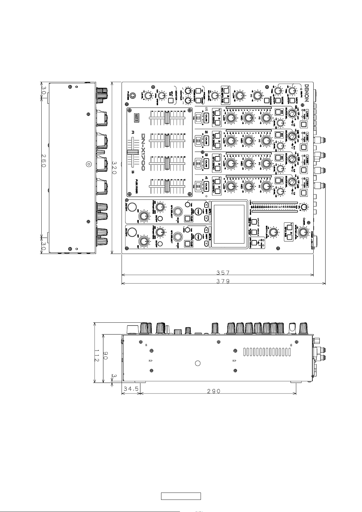
DN-X1700
DIMENSION
4
DN-X1700
WIRE ARRANGEMENT
If wire bundles are untied or moved to perform adjustment or parts replacement etc., be sure to rearrange them neatly as they
were originally bundled or placed afterward.
Otherwise, incorrect arrangement can be a cause of noise generation.
Rear Panel side
5
DN-X1700
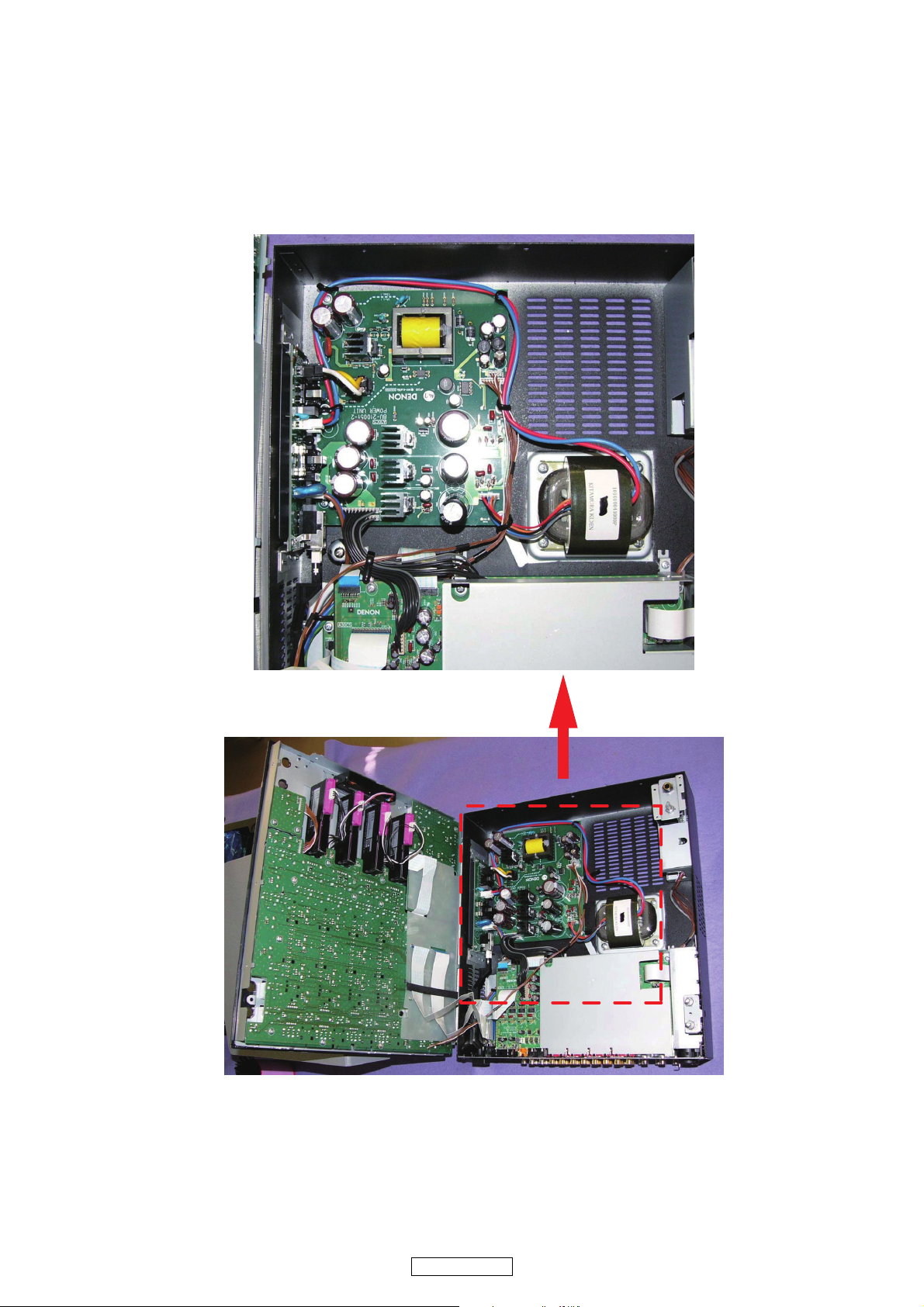
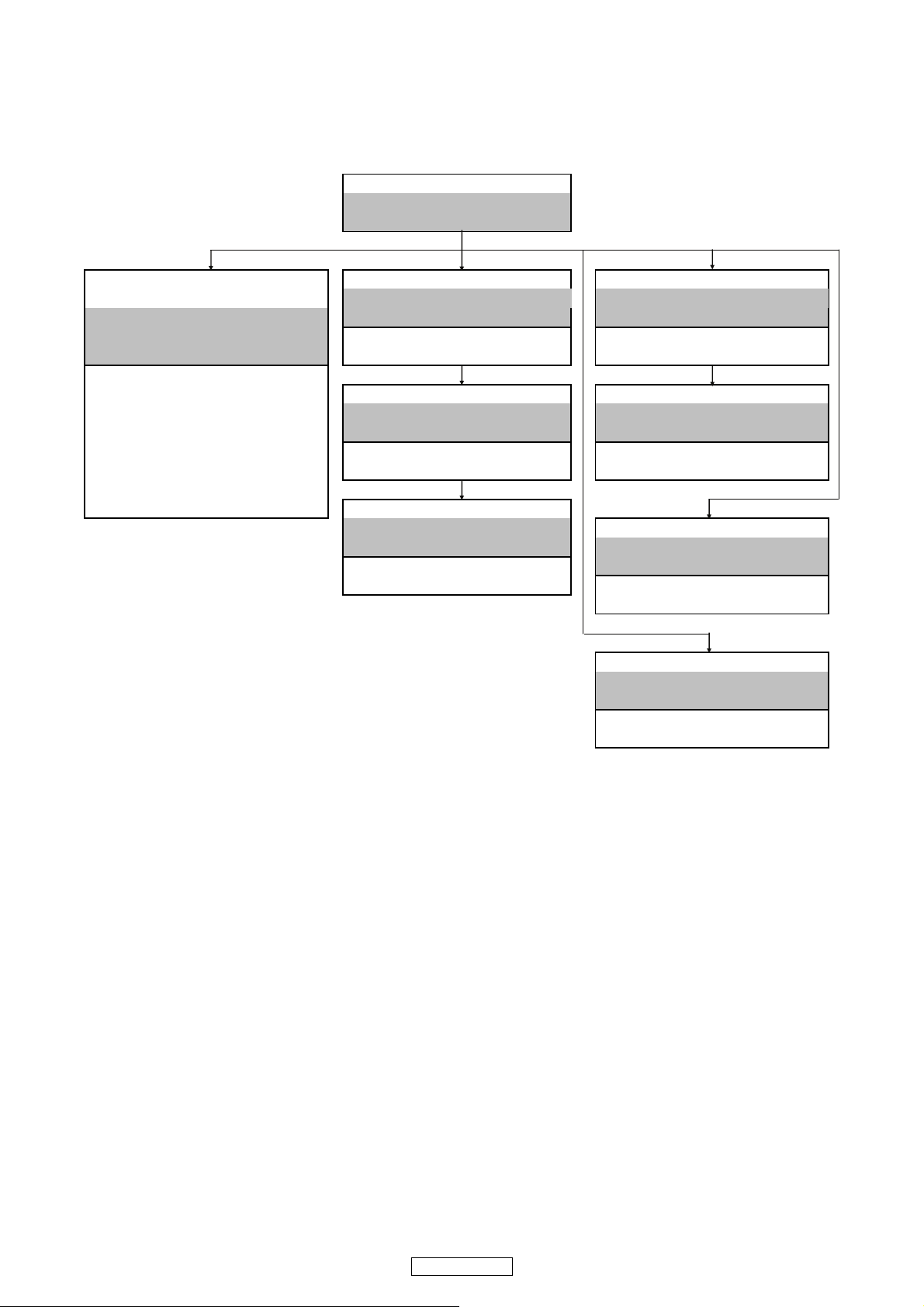
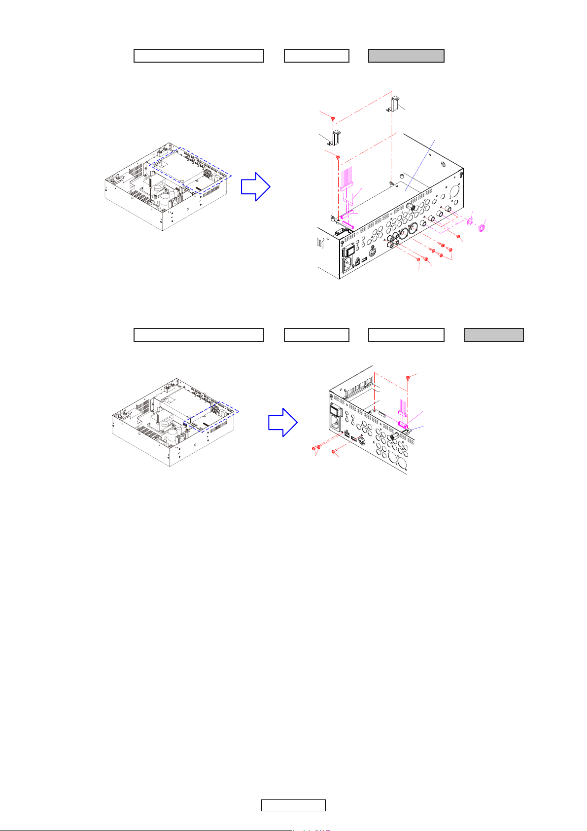
DISASSEMBLY
• Disassemble in order of the arrow of the figure of following flow.
• In the case of the re-assembling, assemble it in order of the reverse of the following flow.
• In the case of the re-assembling, observe "attention of assembling" it.
TOP CHASSIS SUB ASSY
Refer to "DISASSEMBLY 1.TOP CHASSIS
SUB ASSY" and "EXPLODED VIEW"
TOP PANEL UNIT, TOP SUB PANEL UNIT INPUT UNIT POWER SW UNIT
and TOP MONITOR UNIT
Refer to "DISASSEMBLY 3.INPUT UNIT" Refer to "DISASSEMBLY 6.POWER SW UNIT"
Refer to "DISASSEMBLY 2.TOP PANEL UNIT, and "EXPLODED VIEW" and "EXPLODED VIEW"
TOP SUB PANEL UNIT and TOP MONITOR UNIT" INPUT UNIT POWER SW UNIT
and "EXPLODED VIEW" (Ref. No. of EXPLODED VIEW : E) (Ref. No. of EXPLODED VIEW : C-1)
TOP PANEL
(Ref. No. of EXPLODED VIEW : 066)
OUTPUT UNIT POWER UNIT
TOP PANEL UNIT
Refer to "DISASSEMBLY 4.OUTPUT UNIT" Refer to "DISASSEMBLY 7.POWER UNIT"
(Ref. No. of EXPLODED VIEW : A-1) and "EXPLODED VIEW" and "EXPLODED VIEW"
TOP SUB PANEL UNIT OUTPUT UNIT POWER UNIT
(Ref. No. of EXPLODED VIEW : B-1) (Ref. No. of EXPLODED VIEW : F-1) (Ref. No. of EXPLODED VIEW : C-2)
TOP MONITOR UNIT
(Ref. No. of EXPLODED VIEW : A-2)
MAIN UNIT
Refer to "DISASSEMBLY 5.MAIN UNIT"
HP UNIT
and "EXPLODED VIEW" Refer to "DISASSEMBLY 8.HP UNIT"
MAIN UNIT and "EXPLODED VIEW"
(Ref. No. of EXPLODED VIEW : D) HP UNIT
㩷
(Ref. No. of EXPLODED VIEW : B-2)
MIC UNIT
Refer to "DISASSEMBLY 9.MIC UNIT"
and "EXPLODED VIEW"
MIC UNIT
(Ref. No. of EXPLODED VIEW : F-2)
6
DN-X1700
1. TOP CHASSIS SUB ASSY
(1) Remove the KNOBs and screws, then disconnect the FFC cables and connector wires.
2. TOP PANEL UNIT, TOP SUB PANEL UNIT and TOP MONITOR UNIT
(1) Remove the KNOBs.
Proceeding : TOP CHASSIS SUB ASSY
KNOB S
KNOB L
KNOB L
KNOB SEL
KNOB M
KNOB M
KNOB L
KNOB M
KNOB S
KNOB M
KNOB
FADER CH
KNOB
FADER
SCREW
SCREW
SCREW
SCREW
SCREW
KNOB L
KNOB JOG
CX041
FFC Cable
TOP PANEL UNIT, TOP SUB PANEL UNIT and TOP MONITOR UNIT
→
Proceeding : TOP CHASSIS SUB ASSY
KNOB S
KNOB L
KNOB L
KNOB SEL
KNOB M
KNOB M
KNOB L
KNOB M
KNOB S
KNOB
FADER CH
KNOB
FADER
KNOB L
KNOB JOG
7
DN-X1700
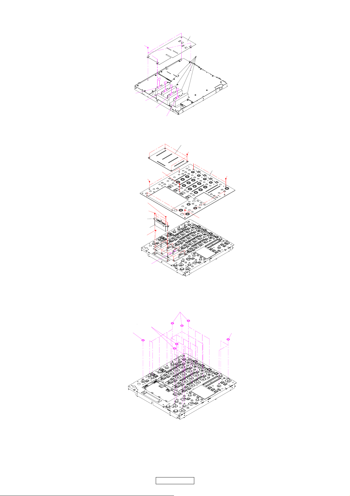
(2) Remove the PUSH RIVET, then detach the PROTECTOR TOP. Disconnect the connector wires.
(3) Remove the screws, then disconnect the connector wire.
(4) Remove the NUTs.
PUSH RIVETS
Bottom View
CW042
CW043
CW045
CW046
PROTECTOR TOP
CH FADER
SCREW
FADER PANEL
SCREW
SCREW
SCREW
SCREW
TOP PANEL SUB ASSY
CX044
SCREW
LR FADER
BRACKET FADER
SCREW
SCREW
NUT
NUT
NUT
NUT
8
DN-X1700
(5) Disconnect the FFC cable, then remove the screws.
3. INPUT UNIT
(1) Remove the PUSH RIVETs and screws, then detach the SHIELD INPUT.
Disconnect the FFC cables and connector wires, then remove the NUTs, WASHERs and screws.
FFC cable
TOP SUB PANEL UNIT
SCREW
SCREW
SCREW
SCREW
TOP MOITOR UNIT
TOP PANEL UNIT
Proceeding : TOP CHASSIS SUB ASSY
INPUT UNIT
→
FFC cable
WASHER
NUT
FFC cable
SCREW
SCREW
SCREW
SHIELD INPUT
CW101
FFC cable
SCREW
SCREW
SCREW
INPUT UNIT
PUSH RIVET
Front side
Back side
9
DN-X1700
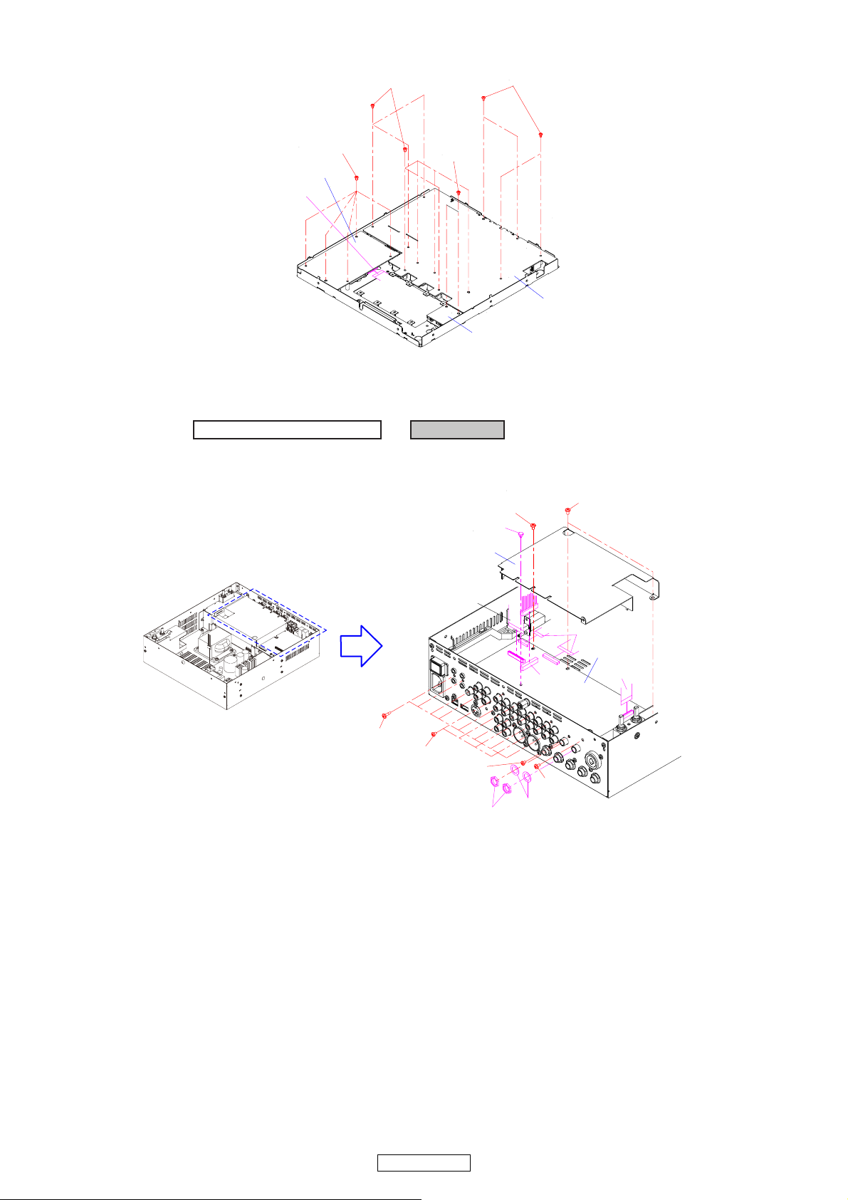
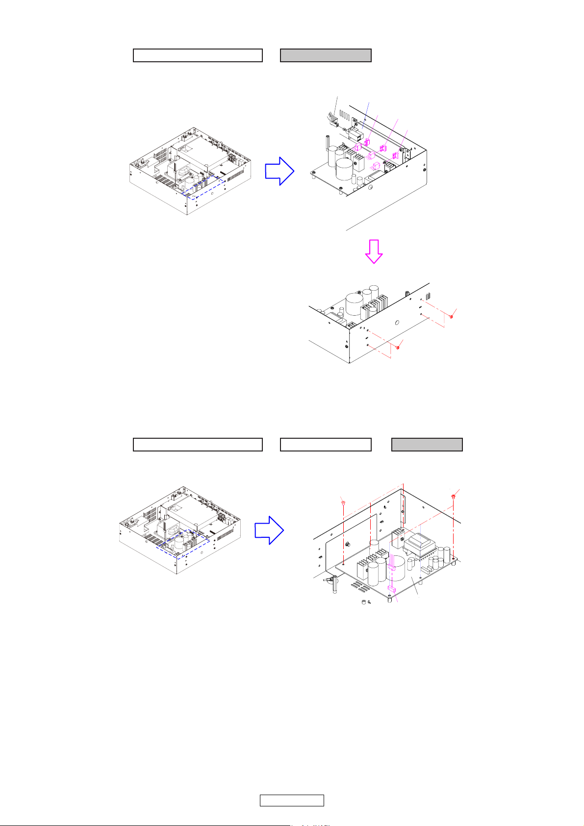
4. OUTPUT UNIT
(1) Disconnect the FFC cable and connector wire, then remove the NUTs, WASHERs and screws.
5. MAIN UNIT
(1) Disconnect the connector wire, then remove the screws.
Proceeding : TOP CHASSIS SUB ASSY
INPUT UNIT
→
OUTPUT UNIT
→
NUT
WASHER
SCREW
SCREW
SCREW
STAY PWB
STAY PWB
SCREW
SCREW
FFC cable
CW102
SCREW
OUTPUT UNIT
Front side
Back side
Proceeding : TOP CHASSIS SUB ASSY
INPUT UNIT
→
OUTPUT UNIT
→
MAIN UNIT
→
%;
5%4'9
/#+070+6
5%4'9
5%4'9
Front side
Back side
10
DN-X1700
6. POWER SW UNIT
(1) Remove the LINK, then disconnect the connector wires. Remove the screws.
7. POWER UNIT
(1) Disconnect the connector wires, then remove the screws.
Proceeding : TOP CHASSIS SUB ASSY
POWER SW UNIT
→
CX023
CX021
POWER SW UNIT
CX022
LINK
SCREWS
SCREWS
Front side
Back side
Proceeding : TOP CHASSIS SUB ASSY
POWER SW UNIT
→
POWER UNIT
→
Front side
Back side
SCREW
CY501
SCREW
POWER UNIT
11
DN-X1700
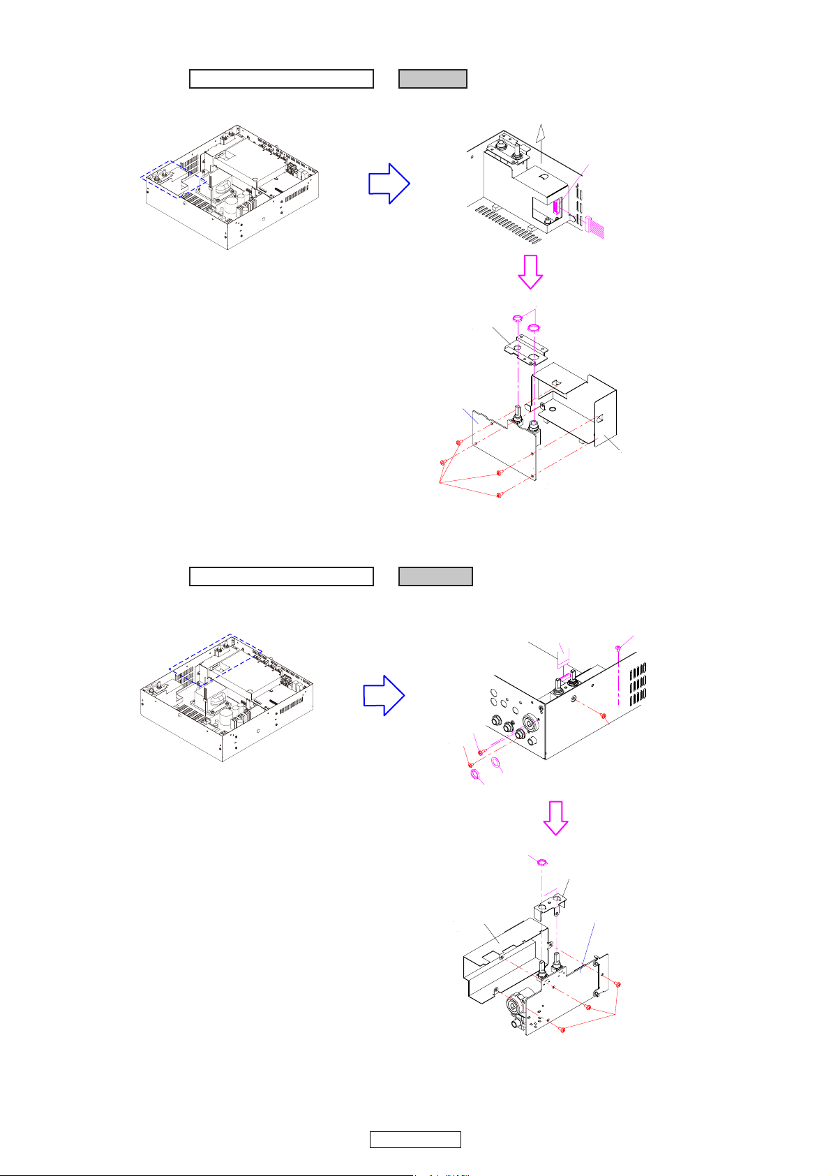
8. HP UNIT
(1) Disconnect the connector wire, then remove the NUTs and screws.
9. MIC UNIT
(1) Disconnect the FFC cable, then remove the NUTs, WASHERs and screws.
Proceeding : TOP CHASSIS SUB ASSY
HP UNIT
→
SCREW
HP UNIT
SHIELD HP
NUT
BRACKET N HP
Front side
Back side
CY103
Proceeding : TOP CHASSIS SUB ASSY
MIC UNIT
→
SCREW
SCREW
NUT
WASHER
SCREW
SCREW
SCREW
SHIELD MIC
MIC UNIT
NUT
BRACKET MIC TOP
Front side
Back side
FFC Cable

12
DN-X1700
SERVICE MODE
1. Launching the service mode and selecting the check mode
• Pressing the MIC1 ON/OFF and MIC EFX INS 1 button simultaneously, turn on the power. Keep pressing the MIC1 ON/
OFF and MIC EFX INS 1 button until [DENON DJ] is displayed. When the service mode is set, the service mode's top
menu appears.
※ The communications mode is set when the power is turned off then turned back on.
• Contents of the display on the service mode's top menu
(1) Function
(2) PANEL_SW
(3) PANEL_VR
(4) PANEL_LED
(5) PANEL_LCD
• Turn the EFX SELECT control of EFX2 to select each check mode, then press the EFX SELECT control to set each check
mode.
Entered items are displayed in blue characters, other items in white characters.
2. Mode
2.1. Function
In the function mode, X1700 Init is the only mode used during servicing.
(Items marked * are for design inspection. Do not use them for servicing purposes.)
• Contents of the display on the function mode's menu
(1) Signal Output *
(2) Digital Input *
(3) X1700 Init
The contents of the preset memory are set to the factory defaults.
q "Execute OK?” is displayed.
w When entered by pressing the EFX2's EFX SELECT control, the "Execute OK?" display changes from white to
blue characters.
e With "Execute OK?" displayed in blue characters, press the EFX2's EFX Select control to execute initialization.
"Complete!!" is displayed when initialization is completed.
(4) LCD GM Setting *
(5) USB R/W Test *
(6) MIDI OUT TEST *
(7) USB host / Device switch
(8) USB Mode Change *
(9) USB Audio Input *
(10)USB Audio Output *
Press the Time (Back) button to return to the top menu of the service mode.
2.2. PANEL_SW (PANEL_SW Check)
• Check the operations of the switches.
(1) In the initial status, all switch displays are off ( □ - white).
(2) When a switch is pressed, the switch display turns on (■ - red).
※ For Source Select 1 ~ 4 and A ⇔ THRU ⇔ B Select 1 ~ 4 Fader Assign, the selected place is displayed as on (
■ - red).
(3) When all switches are pressed and all switch displays are on ( ■ - red), the message "ALL OK! Push EFFECT
SELECT Button" is displayed.
(4) Press the Effect Select 2 button to return to the top menu of the service mode.
※ When the TAP button is pressed while the "PANEL_SW" mode is being executed, the service mode's top menu
reappears.

13
DN-X1700
2.3. PANEL_VR (PANEL VR, FADER VR Check)
• Check the value of VR.
(1) FADER A, B
Fader value A side : 1018 or more Fader value B side : 3 or less
(2) FADER 1ch, 2ch, 3ch, 4ch
Fader value MAX : 1018 or more Fader value MIN : 3 or less
• Check the value of FADER VR.
(1) PAN, CH CONTOUR (L), CROSS CONTOUR(R), MIC LEVEL, LEVEL(LINE1, LINE2, LINE3, LINE4), MASTER
LEVEL, BOOTH LEVEL, DRY/WET(EFX1), DRY/WET(EFX2)
VR value MAX : 1018 or more VR value MIN : 3 or less
(2) MIC EQ (HI), MIC EQ(LOW), LINE1-EQ (HI/MID/LOW ), LINE2-EQ (HI/MID/LOW), LINE3-EQ(HI/MID/LOW),
LINE4-EQ (HI/MID/LOW), BAL, PARAMETERS (EFX1), PARAMETERS (EFX2)
VR value MAX : 1018 or more VR value MIN : 3 or less Central click point : 435~589
Note : The headphones LEVEL, MIC1 TRIM, MIC2 TRIM control are an analog VR, so there is no VR value display.
• Check the operations of the rotation detection of the Effect Select knob.
EFX SELECT(EFX1, EFX2)
When the Effect Select knob is turned counterclockwise : "<" is displayed.
When the Effect Select knob is turned clockwise : ">" is displayed.
Press the EFX SELECT(EFX2) button to return to the top menu of the service mode.
2.4. PANEL_LED (PANEL LED Check)
(Items marked * are for design inspection. Do not use them for servicing purposes.)
• Check the lighting of the LED.
When the TAP button is pressed, the mode changes in the order shown below.
(1) ALL Light : All LEDs Light.
(2) DIM Light : The dimmer function LEDs are set to the dimmer lit status.
CUE1, CUE2, CUE3, CUE4, EFEX SEND(LINE1)1/2, EFEX SEND(LINE2)1/2, EFEX
SEND(LINE3)1/2, EFEX SEND(LINE4)1/2, MIDI CLK, CUE(EFX1), CUE(EFX2), EFEX1 ON/
OFF, EFEX2 ON/OFF
(3) ALL Extinction : All LEDs off.
(4) MAX Lighting * : For design inspection
(5) TYP Lighting * : For design inspection
Press the EFX SELECT(EFX2) button to return to the top menu of the service mode.
2.5. PANEL_LCD (PANEL LCD Check)
• Perform LCD checking and adjustment.
When the TAP button is pressed, the mode changes in the order shown below.
(1) Black screen mode: All black display
(2) White screen mode: All white display
(3) Red screen mode: All red display
(4) Green screen mode: All green display
(5) Blue screen mode: All blue display
(6) Adjustment screen mode: When the Effect Select 2 button is pressed, the black and gray (50%) ratio is adjust-
ed.Adjust to the position at which flickering is minimum.
(Screen displaying black and gray (50%) for each dot).
Press the EFX SELECT(EFX2) button to return to the top menu of the service mode.

14
DN-X1700
VERSION UPGRADE PROCEDURE OF FIRMWARE
Use the procedure described below to update the firmware to a newer version.
• Store the file for updating the firmware in the root directory of USB device.
• If the file for updating the firmware is stored on a USB device, connect the USB device to the USB A terminal.
Note : Do not turn off the power or disconnect the USB cable or the USB device while the firmware is being updated.
If firmware updating is not completed normally, some operations may no longer be guaranteed to work and it may
not be possible to update the firmware again.
(1) Turn on the power while pressing the MIC2 ON/OFF and CKING button simultaneously. (Version up mode)
(2) Press the EFX INS 1 button according to the screen display.
(3) "Ver.* * * * >>> Ver. * * * *" is displayed.
(4) Press the EFX INS 2 button to begin updating.(Approximately 40 second are required for updating to be complet-
ed.)
(5) "Shut the power OFF" is displayed when firmware updating is completed.
(6) Turn the power off and disconnect the USB device from the USB port.
15
DN-X1700
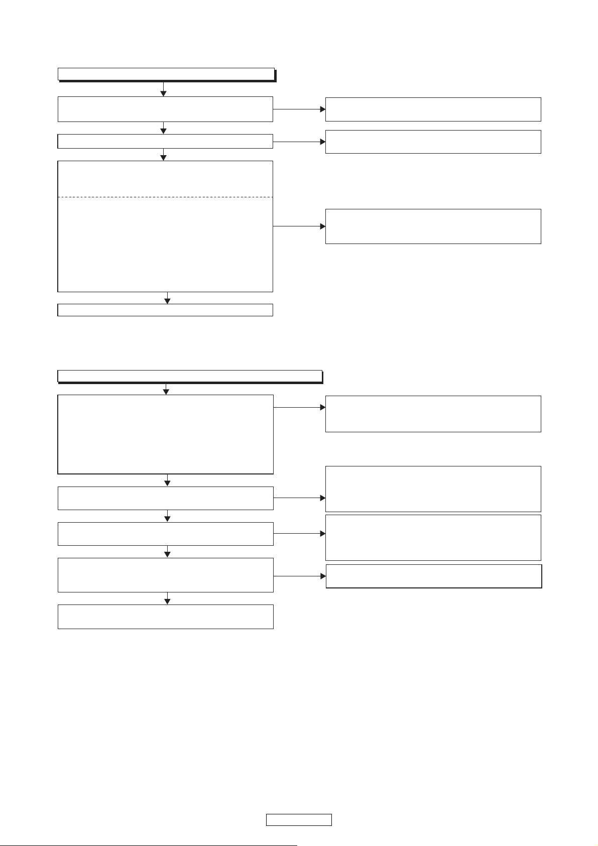
TROUBLE SHOOTING
FLOW CHART NO.1 (8U-210051-1, -2:POWER UNIT)
The power cannot be turned on.
Is the fuse normal?
Is normal state restored when once unplugged
power cord is plugged again after several seconds?
Is the +3.3V line voltage normal?
See FLOW CHART NO.2 <The fuse blows out.>
Check if there is any leak or short-circuiting on the
primary circuit component, and replace it if defective.
(C901,C902,C903,C906,C907,C908,L901,L902,T901)
Check each rectifying circuit of the secondary circuit
and replace it if defective.
Yes
Yes
Yes
No
No
No
FLOW CHART NO.3 (8U-210051-1, -2:POWER UNIT)
Is the +5V line voltage normal?
+1.2V is not outputted.
Check if there is any leak or short-circuiting on the
primary circuit component, and replace it if defective.
(C901,C902,C903,C906,C907,C908,L901,L902,T901)
No
FLOW CHART NO.4 (8U-210051-1, -2:POWER UNIT)
See FLOW CHART
NO.1 <Is the +3.3V line voltage normal?>
+3.3V is not outputted.
FLOW CHART NO.2 (8U-210051-1-2:AC INPUT UNIT, POWER UNIT)
The fuse blows out.
After servicing, replace the fuse.
Check the presence that the primary component
is leaking or shorted and replace it if defective.
Check the presence that the rectifying diode or
circuit is shorted in each rectifying circuit of
secondary side, and replace it if defective.
The fuse blows out.
Check IC903 and the periphery circuit, and replace it
if defective.
Yes
FLOW CHART NO.5 (8U-210051:POWER UNIT)
+15VA is not outputted.
Is the voltage of +15V or more supplied to
IN terminal of IC907?
Check D913,D914,D917,D918 and replace it
if defective.
Check IC907 and the periphery circuit, and replace it
if defective.
Yes
No
Is the fuse normal?
See FLOW CHART NO.2 <The fuse blows out.>
Yes
No
FLOW CHART NO.6 (8U-210051:POWER UNIT)
-15VA is not outputted.
Is the voltage of -15V or less supplied to
IN terminal of IC906?
Check D913,D914,D917,D918 and replace it
if defective.
Check IC906 and the periphery circuit, and replace it
if defective.
Yes
No
Is the fuse normal?
See FLOW CHART NO.2 <The fuse blows out.>
Yes
No

16
DN-X1700
Yes
Yes
Yes
No
No
FLOW CHART NO.7 (8U-310012:MAIN UNIT, 8U-210051:POWER UNIT)
The LCD display does not light up.
Is +5V voltage supplied to 1pin of CX041
on POWER UNIT?
Is +3.3V voltage supplied to 3pin of CX041
on POWER UNIT?
Ia signal outputted from LCD_CS,LCD_D0,LCD_SCK,
LCD_VSYNC,LCD_HSYNC,LCD_CLK,LCD_R0-R4,
LCD_G0
〜G5,LCD_B0〜B4 terminals of IC104
on MAIN UNIT?
Replace the LCD display.
Check the +5V line and service it if defective.
Check the +3.3V line and service it if defective.
No
Replace IC104.
FLOW CHART NO.8 (8U-210034-1:PANEL UNIT)
The key operation is not functioning.
Are the contact point and the installation state of the
key switches (S401~S432), rotary switches (S433~S436),
slide switches (S437~S440) normal?
No
Re-install the switches (S401~S432) correctly
or replace the poor switch.
No
Check the TR101~TR116 and their periphery, and
service it if detective.
Yes
Does LED(LD101~LD325) light correctly ?
Replace IC406.
Yes
Yes
When pressing each key switches, turning rotary
switches and switching slide switches, do the voltage
of each pin of IC406(shown below) increase?
No
Check the key switches (S401~S432) and rotary
switches (S433~S436), slide switches (S437~S440) ,
and their periphery, and service it if detective.
Key switches
S401,407,411,414,419,424,429,432 :IC406 11pin
S404 :IC406 12pin
S409,415,420,425,428,430 :IC406 13pin
S403,415,410,416,421,426,431 :IC406 3pin
S402,406,412,417,422,427
:IC406 4pin
S408,413,418,423 :IC406 5pin
Rotary switches
S433,434,435,436 :IC406 11pin
S433,434,435,436 :IC406 12pin
S433,434,435,436 :IC406 13pin
S433,434,435,436 :IC406 3pin
S
433,434,435,436 :IC406 4pin
Slide switches
S437,438,439,440 :IC406 5pin
S437,438,439,440 :IC406 6pin
17
DN-X1700
No
Check the input signal from CY232 to IC101 and their
periphery, and service it if detective.When the input
signal is correct, IC101 is replaced.
FLOW CHART NO.10 (8U-310017:OUTPUT UNIT)
Function of sound for master output do not operate normally.
Yes
No
Check periphery circuit of IC103,IC106,IC104
from 34pin and 22pin of IC101, and service it
if defective. When the periphery circuit is correct,
IC103,IC106 or IC104 is replaced.
Are the audio signals outputted to 7pin and
1pin of IC103(Lch),IC106(Rch) and IC104(L/Rch)?
Yes
No
Check periphery circuit of IC105,IC107 from 7pin
and 1pin of IC104, and service it if defective.
When the periphery circuit is correct, IC105
or IC107 is replaced.
Are the audio signals outputted to 7pin(COLD) and
1pin(HOT) of IC105(Lch),IC107(Rch)?
Yes
Check periphery circuit of JK101,JK102 from 7pin
and 1pin of IC105,IC107, and
replace
it if defective.
Yes
Is 20pin of CY232 (MUTE control signal)H, and has
been the TR106,TR107 collector (MUTE drive signal)
L(0V)?
Check TR106,TR107 and the periphery circuit,
and service it if defective.
No
FLOW CHART NO.9 (8U-210046-1:EFECT UNIT)
The key operation is not functioning.
No
Check the TR113~TR 116and their periphery, and
service it if detective.
Replace IC601.
Yes
Are the contact point and the installation state of the
key switches (S601~S604) normal?
No
Re-install the switches (S401~S432) correctly
or replace the poor switch.
Yes
Does LED(LD601~LD620) light correctly ?
Yes
When pressing each key switches, pressing and
turning encoder switches, do the voltage
of each pin of IC601(shown below) increase?
No
Check the key switches (S603~S614) and encoder
switches (S615,S616) and their periphery,
and service it if detective.
Key switches
S603,606,608,611 :IC601 11pin
S601,604,609,612 :IC601 12pin
S605,413 :IC601 13pin
S602,607,610,614 :IC601 16pin
Encoder switches(pressing)
S615,616 :IC601 13pin
Encoder switches(turning)
S615,616 :IC601 3,4,5,14pin
・Set the line input selector button to "CD".
・Set the fader assign switch to "THRU".
・Set the channel fader to "MAX".
・Set the master level control to "MAX".
Are audio signals output to IC101 34pin (left channel)
and 22pin (right channel) when an audio signal of
1 kHz 0 dBV is input externally to the CD input?
18
DN-X1700
No
Check the input signal from JK101 to IC102 and their
periphery, and service it if detective.
When the input signal is correct, IC102 is replaced.
FLOW CHART NO.11 (8U-310016:INPUT UNIT)
Function of sound for master output do not operate normally.
Check the input signal RL101 and their periphery,
and service it if detective.
When the input signal is correct, RL101 is replaced.
Yes
No
Are the audio signals outputted to 5pin(Lch) and
6pin(Rch) of RL101?
Yes
No
Are the digital audio signals(0-3.3V) outputted from
15pin(DATA) of IC105(L/Rch)?
Check IC108 and the periphery circuit, and service it
if defective.
When the input signal is correct, IC108 is replaced.
Yes
No
Are the digital audio signals outputted from 3pin
of IC108?
Yes
Check periphery circuit of 12pin of CY231 from
3pin of IC108, and
replace it if defective.
Yes
Is 2pin of CY231 (RELAY control signal)L, and has
been the TR109 collector (RELAY signal) H(+5V)?
Check TR109 and the periphery circuit, and service it
if defective.
No
Check periphery circuit of IC103,IC104 from 5pin and
6pin of RL101, and service it if defective.
When the input signal is correct, IC103,IC104 is replaced.
Yes
No
Are the audio signals outputted to 7pin and
1pin of IC103(Lch),IC104(Rch)?
・Set the line input selector button to "CD".
・Set the fader assign switch to "THRU".
・Set the channel fader to "MAX".
・Set the master level control to "MAX".
Are audio signals output to IC102 7pin (left channel)
and 1pin (right channel) when an audio signal of
1 kHz 0 dBV is input externally to the CD input?
Check that IC105 9pin is "L" (with Fs: 44.1 k) and
that 19pin is "H". Check the signal input to 16pin,
17pin and 18pin.
If there is no input signal, repair the defective part.
When the input signal is correct, IC105 is replaced.
19
DN-X1700
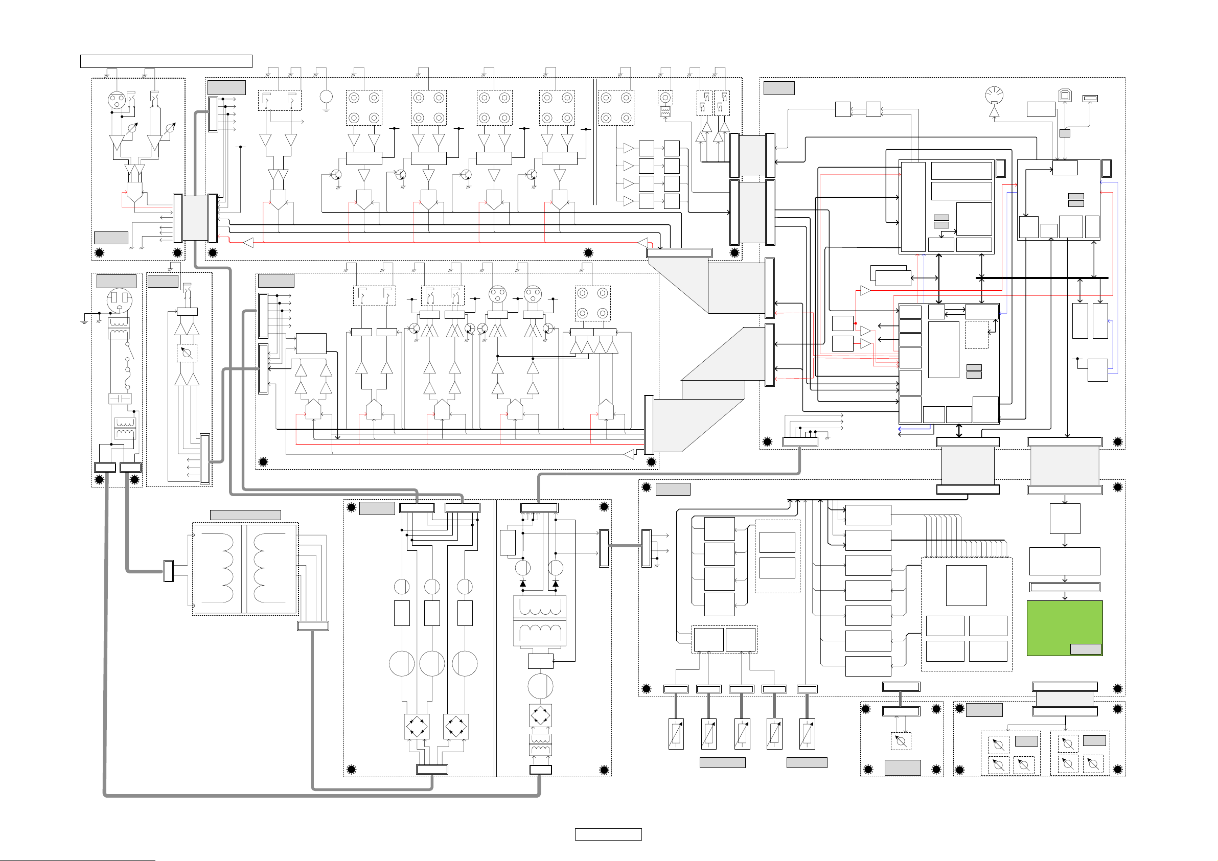
BLOCK DIAGRAM
DNX1700X BLOCK DIAGRAM
CPU
SH7263
DSP
DA710
4MB F-ROM
14pin
14pin
1.2V
DCDC
48MHz
CPU(USB)
16MBx16bit
SDRAM
16MBx16bit
SDRAM
8MBx32bit
SDRAM
SRCDIT
25pin FFC P1.0 Si 27pin FFC P1.0 Si8pin KR
25pin FFC P1.0 Si
8U-310016
INPUT UNIT
8U-310012
MAIN UINT
8U-310017-1
OUTPUT UNIT
8U-210051-2
POWER UNIT
8U-210051-1
AC INPUT UNIT
8U-210034-1
PANEL UNIT
8U-310017-2
MIC UNIT
8U-21046-2
HP UNIT
ADC
ADC
ADC
ADC
Relay Relay Relay Relay
ADC
DAC
DAC
DAC
DAC
ADC
AC-DC
+15V
REG
+5VA
LDO
-15V
REG
25pin FFC P1.0 Si
25pin FFC P1.0 Si
8pin PH10P-SCN
10pin EH
ANALOG TRANS
SELECTOR x 4
CH FADER
LED x 252
VR x 16
VR(C) x 16
TACT SW x 54
SLIDE SW x 4
DIGITAL BLOCK
ANALOG BLOCK
3-8 DEC
SN74HCT138APW
S/P
DRIVER
TB62725BFNG
P/S Buffer
SN74LV165APW
X-FADER
LINE1 PHONO1 LINE2 PHONO2 LINE3 PHONO3 LINE4 PHONO4
RIAA
ST
EFFECT RETURN
L(MONO) R
GND(PHONO)
MUTE MUTEMUTEMUTE
MUTEMUTE
DIGITAL IN
12
34
12
34
MIC1 MIC2
PHONES
EFFECT SEND
LR
BOOTH
LR
MASTER
L
R
MASTER REC
TR
Relay Relay
TR
MUTE MUTE
MUTE
Relay
FADER
MIDI OUT USB B
2pin VH
5pin EH
CLK
SEL
DIR
IF
LED/SW
MTX
FIFO REG
EMIF
LCDC
ADC
USB CTL
SSI
0/1
McASP
0
+3.3V
+1.2V
+3.3V
+1.2V
+3.3V
+1.2V
COM35T3829
32bit MAIN BUS
EMIF
LRCK/BCK
LRCK/BCK
MCLK 16.9344M
ADC_DAC LRCK/BCK
RST
+1.2V
+5VD
RST(soft)
RST
DAC Signal DATA
Digital IN
16.9344
MHz
24.576
MHz
Audio CLK
ADMCLK
DAMCLK
AHCLK
AD CTL
Relay
Fader
BPM&LVL
AD Signal DATA
MCLK/BCK/LRCK for ADC
AD CTL
Digital IN
Relay
Fader
RIAA
RIAA
RIAA
+5VA
+15V
-15V
AGND
AGND
HA HA
Diff
+15V
-15V
AGND
+3.3V
DGND
GND0
+5VD
23pin FFC P1.0 Si
23pin FFC P1.0 Si
DA Signal DATA
DA CTL
MCLK/BCK/LRCK for DA
10pin EH
+5VA
+15V
-15V
AGND
AGND
MUTE
MUTE(TR)
ST
ST
ST
ST
ST
ST
ST
ST
ST
ST
ST
10P-SAN
MUTE
Cirkit
10P-DS
+15V
AGND
-15V
10P-SCN
2pin VH
2pin VH
ADDA
CTL
FFT
4,000LE
POC
LED
Charge pump
64pin FFC P0.5 Au
LCD
CNT
AMP
AMP
SRC
IF
DIT
IF
32bit
UHPI
16bit
32bit 16bit
32bit
2pin VH
Feed Back
+5VD
+3.3V
ENC x 2
8-1
Multiplexer
(TC4051)
8-1
Multiplexer
(TC4051)
8-1
Multiplexer
(TC4051)
3-8 DEC
SN74HCT138APW
S/P
DRIVER
TB62725BFNG
S/P
DRIVER
TB62725BFNG
P/S Buffer
SN74LV165APW
2-1
Multiplexer
2-1
Multiplexer
TC4053
8
8
8
8
8
8
8
3
3
CS
CS
3
3
24
24
24
8-1
Multiplexer
(TC4051)
CPU IF
䋨REG_CS2䋩
FPGA Spartan3A 䋨XC3S400A䋩
LINE
SEL
SSI-DSP
Buffer
TDM-I2S
MONO Det.
SRC
SRC
SRC
SRCDIR
DIR
DIR
DIR
DIGITAL
OUT
23pin FFC P1.0 Si
18pin FFC P1.0 Si
+5VA
+3.3V
DGND
18pin FFC P1.0 Si
Diff
Diff
Diff
Diff
Diff
I-V
I-V
㰿+LPF 㰿+LPF
BTL BTLBTLBTL
㰿+LPF 㰿+LPF
DAC
I-V I-V
㰿+LPF 㰿+LPF
㰿+LPF 㰿+LPF
AK4382
Diff
Diff
Diff
Diff
Diff
AK4399
32bit
PCM1796
PCM1796
AK4382
13pin FFC P1.0 Si
13pin FFC P1.0 Si
24bit
32bit
ADC Signal DATA
U_DATA
Digital IN
ADC DATA
LRCK/BCK
LRCK/BCK
23pin FFC P1.0 Si
DATA
ADDA
LRCK
BCK
UHPI
+3.3V
ADDA CTL
DIT
SRC
DIR
MIX/VR/EQ ect...
DJ EFX
AUTO
BPM
DMA
RL_GND RL_GND RL_GND RL_GND
RL_5V
Digital OUT
RL_GND RL_GND RL_GND
RL_GND
PCM1804 PCM1804 PCM1804
PCM1804
PCM1804
PCM1804
5pin EH
USB A
USB SW
4ch TDM
x2
USB Audio I2S
Selected DATA
Selected DATA CH1䌾4
BUS
I/O
MCLK
RST
ADDA
MUTE/RST
23pin FFC P1.0 Si
23pin FFC P1.0 Si8pin KR
8pin DS
8U-210046-1
EFFECT UNIT
EHR-44P-SCN4P-SCN 4P-SCN 4P-SCN
8U-210034-2
SPLIT UNIT
EFX1
EFX2
4pin KR
4pin DS
+5VA
DGND
+3.3VA
DGND
CX041 CW041
CW102
CW101
CX081
CY051
CY022
CX022 CX023
CY103
CW103
CX102
CX181 CY181
CX101
CY231
CY251
CY131
CX251
CX131
CX231
CX232
CY232
CY081
CX252
CX271
CY252
CY271
CX233
CY271
CW082
CY082
CW046
CW045
CW043
CW042 CX044
27pin FFC P1.0 Si
CX671
LCD
RL_5V
RL_5V RL_5V
RL_5V
RL_5V
RL_5V RL_5V
20
DN-X1700
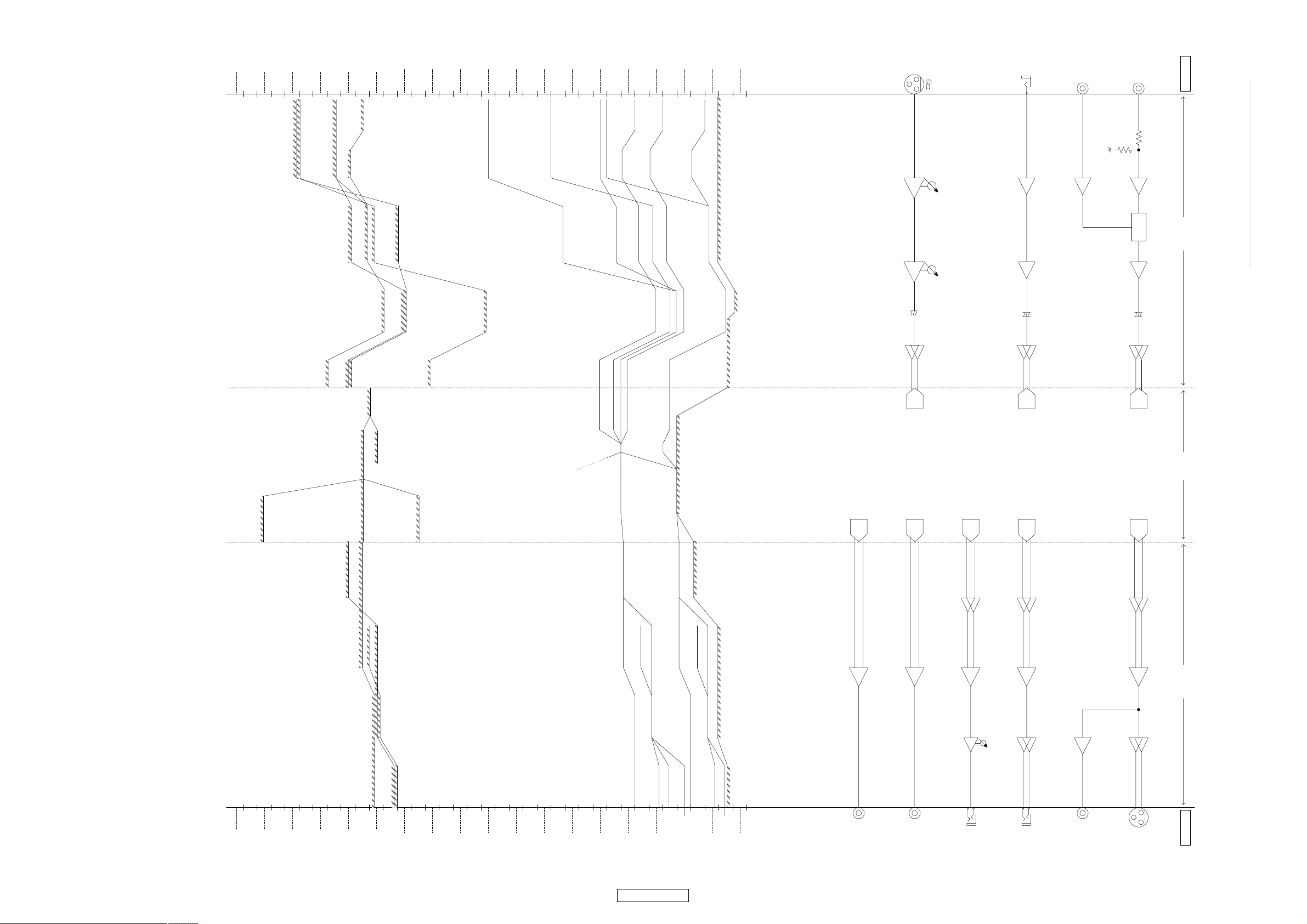
LEVEL DIAGRAM
+30
+20
+10
0
-10
-20
-30
-40
-50
-60
-70
-80
-90
-100
-110
-120
-130
-140
[dBV]
+30
+20
+10
0
-10
-20
-30
-40
-50
-60
-70
-80
-90
-100
-110
-120
-130
-140
[dBu]
Amp
+6.0dB
Diff
+6.0dB
PAD
-20.06dB
ADC
PAD
-4.62dB
VOE=±13.5V=+21.81dBu
+
Vcom=+2.5Voffset
0dBFS
(+7.14dBu)
-4.62dB
3.52dBu
+6.0dB
9.52dBu
-10.54dBu
CD(typ)/EFXRTN(0dBV)
CD/EFXRTN(max)
4.46dBu
EFXRTN(typ)
Diff
-117dBu
-112dBFS
(-104.86dBu)
CD
EFXRTN
-2.68dFS
-17.68dBFS
-97dBu
-109dBu
-10dBV
0dBV
+15dBV
-2.3dB
-20dBFS
+20dB
-∞
CD1~4
0dBV(typ)
+36.07dB
PHONO(typ)
-40dBV
(10mVrms)
-3.93dBu
2.07dBu
-17.99dBu
+5.0dB
-25.13dBFS
PHONO(max)
-20dBV
(100mVrms)
-109.5dBu
-89.5dBu
-93.5dBu
PHONO
-115dBFS
-109.7dBFS
PHONO1~4
10mV(typ)
RIAA
RELAY
+36.07dB
DAC
DAC
DAC
DAC
DAC
1st 2nd
ADC
+
HA HA
Diff
MIC
-60~-20dBu
+6.0dB~+26.5dB +18.0dB~+40.0dB
ADC
+
MIC TRIM(max)
EIN=-127.02dBu
MIC TRIM(min)
+26.30dB
+5.88dB
+19.05dB
+40.13dB
-100.70dBu
-60.57dBu
-80.63dBu
-109.15dBu
-90.10dBu
-110.16dBu
-33.70dBu
-14.12dBu
+6.43dBu
-13.64dBu
-20.78dBFS
-103dBu
MIC(max)
-20dBu
MIC(min)
-60dBu
Σ
MASTER OUT
(XLR)
+4dBu(typ)
PAD+AMP
(-3.41+6.0)
+2.59dB
BTL
+6.0dB
SUM
0dB
AMP
10.35dB
Amp
+6.0dB
Diff
+6.0dB
PAD
-20.06dB
PAD
-20.06dB
EFX RETURN
0dBV(typ)
+2.5V
Offset
+2.5V
Offset
+2.5V
Offset
Σ
Σ
Σ
Σ
MASTER OUT
(RCA)
+0dBu(typ)
BOOTH OUT
+4dBu(typ)
HP OUT
400mW@40hom
REC OUT
-10dBV(typ)
EFX SEND
-10dBV(typ)
I-V
Rf=1.5kohm
I-V
Rf=1.5kohm
SUM
+3.52dB
SUM
+3.52dB
BTL
+6.0dB
VR
-∞~+12dB
SUM
+4.59dB
SUM
+4.59dB
VOE=±13.5V=+21.81dBu
BTL
+30
+10
0
-10
-20
-30
-40
-50
-60
-70
-80
-90
-100
-110
-120
-130
-140
[dBV]
+30
+20
0
-10
-20
-30
-40
-50
-60
-70
-80
-90
-100
-110
-120
-130
-140
[dBu]
INPUT OUTPUT
Diff
MASTER(max)
8.15dBu
18.50dBu
+24dBu
REC/SEND(typ)
-14.22dBV
-1.5dBu
+10.35dB
+4dBu
(XLR/BOOTH)
MASTER(typ)
-11.85dBu
0dBu (RCA)
+20dBu (RCA)
14.74dBu
BOOTH/HP(max)
-5.26dBu
BOOTH/HP(typ)
+10dBu (HP)
REC/SEND(typ)
5.78dBV
+3.52dB
+4.59dB
(XLR/BOOTH)
+10dBV
-10dBV
REC/SEND
-100.5dBu
MASTER
-93.8dBu
-92.8dBu
BOOTH/HP
+20dB
-∞
-150
-150
-150
-150
-139dBFS@24bit
-187.4dBFS@32bit
Analog AnalogDigital
Typical Noise Level ※ Typical Noise Level ※
※ 22Hz-20kHz(SPCL), A-Weighted, FS96kHz
Clip Level
Clip Level
Clip Level
[dBFS] [dBFS]
-20.54dBu -27.68dBFS +7.68dB
21
DN-X1700
SEMICONDUCTORS
Only major semiconductors are shown, general semiconductors etc. are omitted to list.
The semiconductor which described a detailed drawing in a schematic diagram are omitted to list.
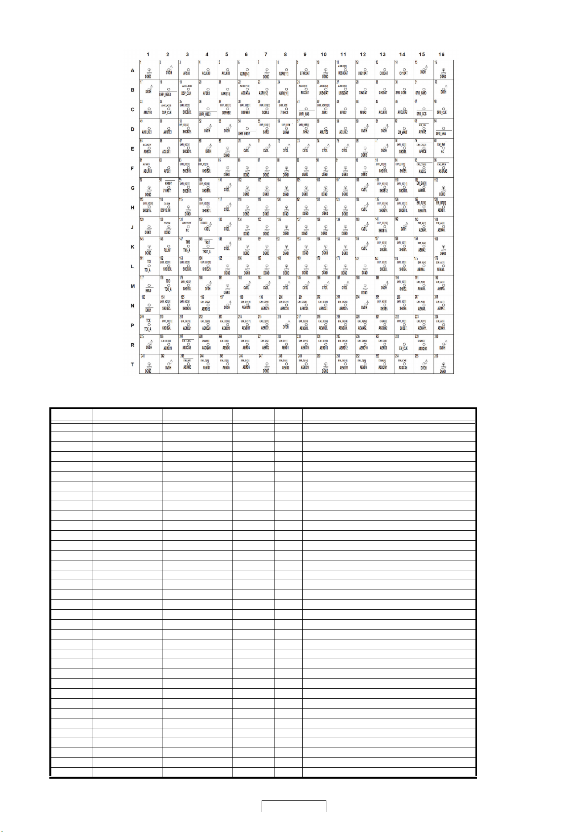
1. IC’s
R5S72630P200FP (IC104)
181
182
183
184
185
186
187
188
189
190
191
192
193
194
195
196
197
198
199
200
201
202
203
204
205
206
207
208
209
210
211
212
213
214
215
216
217
218
219
220
221
222
223
224
225
226
227
228
229
230
231
232
233
234
235
236
237
238
239
240
1
2
3
4
5
6
7
8
9
10
11
12
13
14
15
16
17
18
19
20
21
22
23
24
25
26
27
28
29
30
31
32
33
34
35
36
37
38
39
40
41
42
43
44
45
46
47
48
49
50
51
52
53
54
55
56
57
58
59
60
180
179
178
177
176
175
174
173
172
171
170
169
168
167
166
165
164
163
162
161
160
159
158
157
156
155
154
153
152
151
150
149
148
147
146
145
144
143
142
141
140
139
138
137
136
135
134
133
132
131
130
129
128
127
126
125
124
123
122
121
120
119
118
117
116
115
114
113
112
111
110
109
108
107
106
105
104
103
102
101
100
99
98
97
96
95
94
93
92
91
90
89
88
87
86
85
84
83
82
81
80
79
78
77
76
75
74
73
72
71
70
69
68
67
66
65
64
63
62
61
QFP3232-240Cu
(Top view)
PB2/SCL1/PINT2/IRQ2
PB3/SDA1/PINT3/IRQ3
PVcc
PVcc
PB4/SCL2/PINT4/IRQ4
PB5/SDA2/PINT5/IRQ5
PVss
Vss
PB6/SCL3/PINT6/IRQ6
PB7/SDA3/PINT7/IRQ7
Vcc
PD15/D31/PINT7/SD_CD/ADTRG/TIOC4D
PD14/D30/PINT6/SD_WP/TIOC4C
PD13/D29/PINT5/SD_D1/TEND1/TIOC4B
PD12/D28/PINT4/SD_D0/DACK1/TIOC4A
PVss
PD11/D27/PINT3/SD_CLK/DREQ1/TIOC3D
PVcc
PD10/D26/PINT2/SD_CMD/TEND0/TIOC3C
PD9/D25/PINT1/SD_D3/DACK0/TIOC3B
PD8/D24/PINT0/SD_D2/DREQ0/TIOC3A
PD7/D23/IRQ7/SCS1/TCLKD/TIOC2B
PD6/D22/IRQ6/SSO1/TCLKC/TIOC2A
Vcc
PD5/D21/IRQ5/SSI1/TCLKB/TIOC1B
Vss
PVss
PD4/D20/IRQ4/SSCK1/TCLKA/TIOC1A
PVcc
PD3/D19/IRQ3/SCS0/DACK3/TIOC0D
PD2/D18/IRQ2/SSO0/DREQ3/TIOC0C
PD1/D17/IRQ1/SSI0/DACK2/TIOC0B
PD0/D16/IRQ0/SSCK0/DREQ2/TIOC0A
D15
D14
PVss
D13
PVcc
D12
D11
D10
D9
D8
Vcc
D7
Vss
PVss
D6
PVcc
D5
D4
D3
D2
D1
D0
PVss
PVcc
PC13/RD/WR
PC12/CKE
PC11/CASU/BREQ/AUDATA1
PC10/RASU/BACK/AUDATA0
PC9/CASL
PC8/RASL
Vcc
PC7/WE3/DQMUU/AH/ICIOWR
Vss
PVss
PC6/WE2/DQMUL/ICIORD
PVcc
PC5/WE1/DQMLU/WR
CS0
RD
PC4/WE0/DQMLL
PC3/CS3
PC2/CS2
Vcc
PC0/A0/CS7/AUDSYNC
Vss
PVss
PC1/A1
PVcc
A2
A3
A4
A5
A6
A7
A8
PVcc
A9
PVss
Vss
A10
Vcc
A11
A12
A13
A14
A15
A16
PVss
A17
PVcc
A18
A19
A20
PE2/A21/SCK0
PE3/A22/SCK1
PE0/BS/RxD0/ADTRG
CKIO
Vcc
Vss
PVss
PVcc
XTAL
EXTAL
NMI
PLLVss
RES
PLLVcc
PB1/SDA0/PINT1/IRQ1
PB0/SCL0/PINT0/IRQ0
TCK
TDO
TRST
ASEBRKAK/ASEBRK
TDI
PVcc
TMS
PVss
Vss
PF0/TCLKA/LCD_DATA0/SSCK0
Vcc
PF1/TCLKB/LCD_DATA1/SSI0
PF2/TCLKC/LCD_DATA2/SSO0
PF3/TCLKD/LCD_DATA3/SCS0
PF4/FWE/LCD_DATA4/SSCK1
PF5/FCDE/LCD_DATA5/SSI1
PF6/FOE/LCD_DATA6/SSO1
PF7/FSC/LCD_DATA7/SCS1
PF8/NAF0/LCD_DATA8/SD_D2
PVcc
PF9/NAF1/LCD_DATA9/SD_D3
PVss
Vss
PF10/NAF2/LCD_DATA10/SD_CMD
Vcc
PF11/NAF3/LCD_DATA11/SD_CLK
PF12/NAF4/LCD_DATA12/SD_D0
PF13/NAF5/LCD_DATA13/SD_D1
PF14/NAF6/LCD_DATA14/SD_WP
PF15/NAF7/LCD_DATA15/SD_CD
PF16/FRB/LCD_DON
PF17/FCE/LCD_CL1
PVcc
PF23/SSIDATA1/LCD_VEPWC/AUDATA3
PVss
Vss
PF22/SSIWS1/LCD_VCPWC/AUDATA2
Vcc
PF21/SSISCK1/LCD_CLK
PF20/SSIDATA0/LCD_FLM
PF19/SSIWS0/LCD_M_DISP
PF18/SSISCK0/LCD_CL2
PF24/SSISCK2
PF25/SSIWS2
PF26/SSIDATA2
PVcc
AUDIO_X2
AUDIO_X1
PVss
Vss
PF30/AUDIO_CLK
Vcc
PF27/SSISCK3
PF28/SSIWS3
PF29/SSIDATA3
PVcc
PB12/WDTOVF/IRQOUT/REFOUT/UBCTRG/AUDCK
PVss
AVss
PA7/AN7/DA1
PA6/AN6/DA0
PA5/AN5
AVref
PA4/AN4
AVcc
PA3/AN3
PA2/AN2
PA1/AN1
PA0/AN0
USBDVss
USBDVcc
USBAPVcc
USBAPVss
REFRIN
USBAVss
USBAVcc
VBUS
DP
DM
USBDPVcc
USBDPVss
MD_CLK0
MD_CLK1
PVcc
USB_X2
USB_X1
PVss
Vss
MD
Vcc
PB11/CTx1/IETxD
PB10/CRx1/IERxD
PB9/CTx0/CTx0&CTx1
PB8/CRx0/CRx0/CRx1
PVss
PE15/IOIS16/RTS3
PE14/CS1/CTS3
PE13/TxD3
PVcc
RTC_X2
RTC_X1
PVss
Vss
PC14/WAIT
Vcc
PE12/RxD3
PE11/CS6/CE1B/IRQ7/TEND1
PE10/CE2B/IRQ6/TEND0
PE9/CS5/CE1A/IRQ5/SCK3
PE7/FRAME/IRQ3/TxD2/DACK1
PE6/A25/IRQ2/RxD2/DREQ1
PVcc
PE5/A24/IRQ1/TxD1/DACK0
PVss
PE4/A23/IRQ0/RxD1/DREQ0
PE1/CS4/MRES/TxD0
PE8/CE2A/IRQ4/SCK2
ASEMD
22
DN-X1700
R5S72630P200FP Block Diagram
R5S72630P200FP Terminal Function
Pin No Pin name I/O Pol Function
1 PC10/RASU O FADER CUE 4 OUTPUT
2 /CASL O N SDRAM(IC107) / Column Adress Strobe
3 /RASL O N SDRAM(IC107) / Row Adress Storbe
4VCC VCC
5 DQMUU O SDRAM(IC107) / Input/Output Mask
6 VSS DGND
7 PVSS DGND
8 DQMUL O SDRAM(IC107) / Input/Output Mask
9PVCC PVCC
10 DQMLU O SDRAM(IC107) / Input/Output Mask
11 /CS0 O N FLASH(IC103) / Chip Enable
12 /RD O N FLASH(IC103) /Output Enable, ADSP / UHPI Select Signals
13 DQMLL, /WE0 O SDRAM(IC107) / Input/Output Mask 1, ADSP UHPI Select Signals
14 PC3/CS3 O N SDRAM(IC107) / Chip Select
15 PC2/CS2 O N FPGA / Panel scan signal
16 VCC VCC
17 PC0/A0/CS7 O N FPGA / Chip Select
18 VSS DGND
19 PVSS DGND
20 PC1/A1 O FLASH(IC103), FPGA / Address Bus
21 PVCC PVCC
22 A2 O SDRAM(IC107),FLASH(IC103) / Address Bus
23 A3 O SDRAM(IC107),FLASH(IC103) / Address Bus
24 A4 O SDRAM(IC107),FLASH(IC103) / Address Bus
25 A5 O SDRAM(IC107),FLASH(IC103) / Address Bus
26 A6 O SDRAM(IC107),FLASH(IC103) / Address Bus
27 A7 O SDRAM(IC107),FLASH(IC103) / Address Bus
28 A8 O SDRAM(IC107),FLASH(IC103) / Address Bus
SH-2A
CPU core
Pin function
controller
(PFC)
I/O ports
Clock pulse
generator
(CPG)
Interrupt
controller
(INTC)
Compare
match
timer
(CMT)
Multi-function
timer pulse
unit 2
(MTU2)
Watchdog
timer
(WDT)
Realtime
clock
(RTC)
Internal CPU bus
(IC bus)
Internal DMA bus
(ID bus)
Peripheral bus (P clock)
Por t Port Po rt Por t Port Por t
General I/O EXTAL input
XTAL output
CKIO I/O
Clock mode input
RTC_X1 input
RTC_X2 output
RES input
MRES input
MMI input
IRQ input
PINT input
IRQOUT output
Timer pulse I/O
WDTOVF
output
DREQ input
DACK output
TEND output
Cache
controller
Instruction
cache memory
8 Kbytes
Operand
cache memory
8 Kbytes
On-chip RAM
(high-speed)
64 Kbytes
User
debugging
interface
(H-UDI)
Por t
JTAG I/O
Power-down
mode
control
On-chip RAM
(retention)
16 Kbytes
SD host
interface
(SDHI)
Por t
SD card I/F I/O
Sampling
rate
converter
(SRC)
AND/NAND
flash memory
controller
(FLCTL)
Por t
Flash memory
I/F I/O
D/A converter
(DAC)
Por t
Analog output
A/D converter
(ADC)
Por t
Analog input
ADTRG input
IEBusTM
controller
(IEB)
Por t
IEBus input
Controller
area
network
(RCAN-TL1)
Por t
CAN bus I/O
Serial
sound
interface
(SSI)
Por t
Serial I/O
Audio clock input
Serial
communication
interface with FIFO
(SCIF)
I
2
C bus
interface 3
(IIC3)
Por t Por t Por t
Serial I/O Serial I/O
Internal LCD bus
(IL bus)
LCD I/F I/O
CD-ROM
decoder
(ROM-DEC)
USB2.0 host/
function module
(USB)
Por t
USB bus I/O
USB clock input
Bus state
controller
(BSC)
Por t
External bus I/O
External bus width
mode input
User break
controller
(UBC)
UBCTRG output
LCD
controller
(LCDC)
Peripheral
bus controller
Direct memory
access
controller
(DMAC)
Floating-point
unit (FPU)
Internal bus
(I bus)
(B clock)
Por t
Por t
Por t
CPU bus
(C bus)
(I clock)
CPU memory access bus (M bus)
CPU instruction fetch bus (F bus)
Synchronous
serial commnication
unit
(SSU)
I
2
C bus I/O

23
DN-X1700
29 PVCC P
30 A9 O SDRAM(IC107),FLASH(IC103) / Address Bus
31 PVSS DGND
32 VSS DGND
33 A10 O SDRAM(IC107),FLASH(IC103) / Address Bus
34 VCC VCC
35 A11 O SDRAM(IC107),FLASH(IC103) / Address Bus
36 A12 O SDRAM(IC107),FLASH(IC103) / Address Bus
37 A13 O FLASH(IC103) /Adress Bus
38 A14 O FLASH(IC103) /Adress Bus
39 A15 O FLASH(IC103) /Adress Bus
40 A16 O FLASH(IC103) /Adress Bus
41 PVSS DGND
42 A17 O FLASH(IC103) /Adress Bus
43 PVCC PVCC
44 A18 O FLASH(IC103) /Adress Bus
45 A19 O FLASH(IC103) /Adress Bus
46 A20 O FLASH(IC103) /Adress Bus
47 PE2 O FLASH(IC103) /Adress Bus
48 PE3 O FPGA Configration CCLK
49 /BS/ADTRG I N FPGA /ADTRG
50 CKIO O SDRAM(IC107) CLK/FPGA MCLK
51 VCC VCC
52 VSS DGND
53 PVSS DGND
54 PVCC PVCC
55 XTAL NC
56 EXTAL I 16.9344MHz Input
57 NMI I AC Power Detected Signals (P-Fail)
58 PLLVSS DGND
59 /RES I N CPU RST
60 PLLVCC P
61 /ASEMD I N JTAG
62 PE8/IRQ4 I Interrupt signal
63 CS4 O MIDI Output ClockÅiBPM)
64 PE4/DREQ0 O LCD Serial Control
65 PVSS DGND
66 PE5/DACKO O FPGA Configration
67 PVCC PVCC
68 PE6/RXD2 I UART (Serial Control)
69 PE7/TXD2 O UART (Serial Control)
70 PE9/CS5 O Clock for LCD Serial Control
71 PE10 I FPGA Configration
72 PE11/CS6 O N UHPI Select Signals
73 PE12/RXD3 O FADER PLAY 3 Output
74 VCC VCC
75 /WAIT I N ADSP HRDY
76 VSS DGND
77 PVSS DGND
78 RTC_X1 DGND
79 RTC_X2 NC
80 PVCC PVCC
81 PE13/TXD3 O LCD Serial Control DATA
82 CS1 O FPGA Configration
83 PE15 I FPGA Configration
84 PVSS DGND
85 PB8 I CPU-DSP FLAGÅibackup)
86 PB9 I USB Control
87 PB10 O USB Control
88 PB11 O USB Control
89 VCC VCC
90 MD I MODE Select Åi1:32bit/0ÅF16bitÅj
91 VSS DGND
92 PVSS DGND
93 USB_X1 I X'tal Port for USB(48MHz)
94 USB_X2 O X'tal Port for USB(48MHz)
95 PVCC PVCC
96 MD_CLK1 DGND
97 MD_CLK0 DGND
98 USBDPVSS DGND
99 USBDPVCC USBDPVCC
100 DM I/O USB(B) D- Terminal
101 DP I/O USB(B) D+ Terminal
102 VBUS I VBUS Detected Terminal
Pin No Pin name I/O Pol Function
24
DN-X1700
103 USBAVCC USBAVCC
104 USBAVSS DGND
105 REFRIN I Reference Input (USB)
106 USBAPVSS DGND
107 USBAPVCC USBAPVCC
108 USBDVCC USBDVCC
109 USBDVSS DGND
110 AN0 I CH FADER 1/2 INPUT
111 AN1 I CH FADER 3/4 INPUT
112 AN2 I X FADER INPUT
113 AN3 I CH1 VR INPUT
114 AVCC AV CC
115 AN4 I CH2 VR INPUT
116 AVREF I Transrated Reference Voltage Input
117 AN5 I CH3 VR INPUT
118 AN6/DA0 I CH4 VR INPUT
119 AN7/DA1 O LCD Backlight LED MOD.
120 AVSS DGND
121 PVSS DGND
122 /WDTOVF O LCD Backlight LED ON/OFF SEL
123 PVCC PVCC
124 SSIDATA3 O FPGA / USB Audio data
125 SSIWS3 I FPGA / USB Audio LR clock
126 SSISCK3 I FPGA / USB Audio Bit clock
127 VCC VCC
128 AUDIO_CLK I FPGA / Audio Clock
129 VSS DGND
130 PVSS DGND
131 AUDIO_X1 DGND
132 AUDIO_X2 NC
133 PVCC PVCC
134 SSIDATA2 O FPGA / USB Audio data
135 SSIWS2 I FPGA / USB Audio LR clock
136 SSISCK2 I FPGA / USB Audio Bit clock
137 PF18/LCD_CL2 O LCD CLK
138 PF19/LCD_CL2 O FADER PLAY1 OUTPUT
139 PF20/LCD_M_DISP O LCD VSYNC
140 PF21/SSI/SCLK1 O FADER CUE2 OUTPUT
141 VCC VCC
142 PF22/SSIWS1 O FADER PLAY2 OUTPUT
143 VSS DGND
144 PVSS DGND
145 PF23/SSI/DATA1 O FADER CUE3 OUTPUT
146 PVCC PVCC
147 PF17/LCD_CL1 O LCD HSYNC
148 PF16/LCD_DON O FADER CUE1 OUTPUT
149 PF15/SD_CD O LCD Control Bus
150 PF14/SD_WP O LCD Control Bus
151 PF13_SD_D0 O LCD Control Bus
152 PF12/SD_D0 O LCD Control Bus
153 PF11/SD_SCLK O LCD Control Bus
154 VCC VCC
155 PF10/SD_SCLK O LCD Control Bus
156 VSS DGND
157 PVSS DGND
158 PF9/SD_D2 O LCD Control Bus
159 PVCC PVCC
160 PF8/SD_D2 O LCD Control Bus
161 PF7/SCS1 O LCD Control Bus
162 SS01 O LCD Control Bus
163 PF5/SSI1 O LCD Control Bus
164 SSCK0 O LCD Control Bus
165 PF3/SCS0 O LCD Control Bus
166 SSO0 O LCD Control Bus
167 PF1/SSI0 O LCD Control Bus
168 VCC VCC
169 SSCK0 O LCD Control Bus
170 VSS DGND
171 PVSS DGND
172 TMS I JTAG (for Test Mode)
173 PVCC PVCC
174 TDI I JTAG (for Test Mode)
175 /ASEBRKAK I/O N JTAG (for Test Mode)
176 /TRST I N JTAG (for Test Mode)
Pin No Pin name I/O Pol Function
25
DN-X1700
177 TDO O JTAG (for Test Mode)
178 TCK I JTAG (for Test Mode)
179 PB0/IRQ0 I FPGA / Interrupt signal
180 PB1/IRQ1 I ADSP / Interrupt signal
181 PB2/IRQ2 I/O ADSP / IIC control Clock
182 PB3/IRQ3 I/O ADSP / IIC control data
183 PVCC PVCC
184 PVCC PVCC
185 PB4/SCL2 NC (Pull Up)
186 PB5/SDA2 NC (Pull Up)
187 PVSS DGND
188 VSS DGND
189 PB6/SCL3 NC (Pull Up)
190 PB7/SDA3 NC (Pull Up)
191 VCC VCC
192 PD15/D31 I/O SDRAM(IC107),ADSP / Data Bus
193 PD13/D30 I/O SDRAM(IC107),ADSP / Data Bus
194 D29/TIOC4B I/O SDRAM(IC107),ADSP / Data Bus
195 D28/TIOC4A I/O SDRAM(IC107),ADSP / Data Bus
196 PVSS DGND
197 PD11/D27 I/O SDRAM(IC107),ADSP / Data Bus
198 PVCC PVCC
199 PD10/D26 I/O SDRAM(IC107),ADSP / Data Bus
200 D25/TIOC3B I/O SDRAM(IC107),ADSP / Data Bus
201 D24/TIOC3A I/O SDRAM(IC107),ADSP / Data Bus
202 D23/TCLKD I/O SDRAM(IC107),ADSP / Data Bus
203 D22/TCLKC I/O SDRAM(IC107),ADSP / Data Bus
204 VCC VCC
205 D21/TCLKB I/O SDRAM(IC107),ADSP / Data Bus
206 VSS DGND
207 PVSS DGND
208 D20/TCLKA I/O SDRAM(IC107),ADSP / Data Bus
209 PVCC PVCC
210 PD3/D19 I/O SDRAM(IC107),ADSP / Data Bus
211 PD2/D18 I/O SDRAM(IC107),ADSP / Data Bus
212 D17/TIOC0B I/O SDRAM(IC107),ADSP / Data Bus
213 D16/TIOC0A I/O SDRAM(IC107),ADSP / Data Bus
214 D15 I/O FLASH(103),ADSP / Data Bus
215 D14 I/O FLASH(103),ADSP / Data Bus
216 PVSS DGND
217 D13 I/O FLASH(103),ADSP / Data Bus
218 PVCC PVCC
219 D12 I/O FLASH(103),ADSP / Data Bus
220 D11 I/O FLASH(103),ADSP / Data Bus
221 D10 I/O FLASH(103),ADSP / Data Bus
222 D9 I/O FLASH(103),ADSP / Data Bus
223 D8 I/O FLASH(103),ADSP / Data Bus
224 VCC VCC
225 D7 I/O FLASH(103),ADSP / Data Bus
226 VSS DGND
227 PVSS DGND
228 D6 I/O FLASH(103),ADSP / Data Bus
229 PVCC PVCC
230 D5 I/O FLASH(103),ADSP / Data Bus
231 D4 I/O FLASH(103),ADSP / Data Bus
232 D3 I/O FLASH(103),ADSP / Data Bus
233 D2 I/O FLASH(103),ADSP / Data Bus
234 D1 I/O FLASH(103),ADSP / Data Bus
235 D0 I/O FLASH(103),ADSP / Data Bus
236 PVSS DGND
237 PVCC PVCC
238 RD/WR O SDRAM(IC107) /Write Enable, ADSP UHPI / Select Signals
239 CKE O SDRAM(IC107) / Clock Enable
240 /CASU/BREQ O FADER PLAY4 OUTPUT
Pin No Pin name I/O Pol Function
26
DN-X1700
D710E001ZDH300 (IC501)
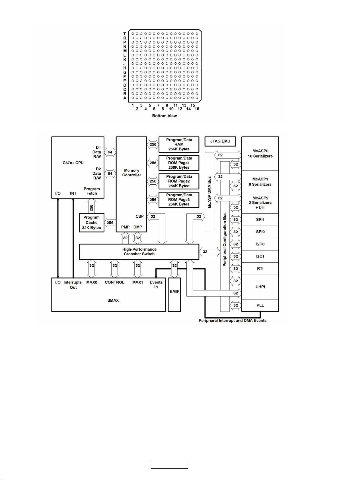
D710E001ZDH300 Block diagram
㪛㪎㪈㪇㪜㪇㪇㪈㪱㪛㪟㪊㪇㪇㩷㪧㫀㫅㩷㪝㫌㫅㪺㫋㫀㫆㫅
27
DN-X1700
D710E001ZDH300 Pin Function
D710E001ZDH300 Terminal Function
Pin No BGA Location Pin name I/O Pol Function
1A1 DGND DGND
2 A2 DVDH DVDH
3 A3 710LRCK O ALL Device LRCK
4 A4 710BCK O ALL Device BCK
5 A5 ACLKR0 IO Not use
6 A6 EFXSDAT O Effect Send Data Output
7A7 DGND DGND
8 A8 BOOTDAT O Booth Out Data Output
9 A9 EFXRDAT I Effect Return Data Input
10 A10 DGND DGND
11 A11 USB3DAT I USB3 Data Input
12 A12 USB1DAT I USB1 Data Input
13 A13 CH3DAT I CH3 Data Input
14 A14 CH1DAT I CH1 Data Input
15 A15 DVDH DVDH
16 A16 DGND DGND
17 B1 DVDH DVDH
18 B2 HUPI_HBE3 I N UHPI Byte Enable for UHPI_HD[31:24]
19 B3 DSP_CLK I McASP0 Receive Master Clock
20 B4 AFSR0 IO Not use
21 B5 SRCDAT O Digital Out Data Output
22 B6 PHONDAT O HeadPhone Data Output
23 B7 RECDAT O Rec Out Data Output
24 B8 MASTDAT O Master Out Data Output
25 B9 MICDAT I Mic Data Input
26 B10 USB4DAT I USB4 Data Input
27 B11 USB2DAT I USB2 Data Input
28 B12 CH4DAT I CH4 Data Input
29 B13 CH2DAT I CH2 Data Input
30 B14 SPIO_SOMI IO IIC control data DSP-CPU
31 B15 DSPGPIO2 I GPIO DSP-FPGA
32 B16 DVDH DVDH
33 C1 AMUTE0 O Not use
34 C2 DSP_CLK I McASP0 Transmit Master Clock
35 C3 SHDB23 IO UHPI Data Bus [Upper 16 Bits (IO)]
36 C4 HUPI_HBE2 I N UHPI Byte Enable for UHPI_HD[23:16]
28
DN-X1700
37 C5 DSPHBE I UHPI Byte Enable for UHPI_HD[15:8]
38 C6 DSPHBE I UHPI Byte Enable for UHPI_HD[7:0]
39 C7 DQMLL I N UHPI Select Signals
40 C8 710HCS I N UHPI Select Signals
41 C9 UHPI_HAS I N UHPI Host Address Strobe
42 C10 SHA3 I UHPI Control Inputs Select Access Mode
43 C11 AFSX2 I Not use
44 C12 AFSR2 I Not use
45 C13 ACLKR2 I Not use
46 C14 DSPGPIO1 I GPIO port DSP-FPGA
47 C15 DSPINT1 O N Interrupt port DSP-FPGA
48 C16 SPIO_CLK IO IIC control clk DSP-CPU
49 D1 AHCLKX1 I Not use
50 D2 AMUTE1 I Not use
51 D3 SHDB22 IO UHPI Data Bus [Upper 16 Bits (IO)]
52 D4 DVDH DVDH
53 D5 DVDH DVDH
54 D6 UHPI_HRDY O N UHPI Ready Output
55 D7 SHRD I N UHPI Select Signals
56 D8 SHRW I N UHPI Read/not Write Input
57 D9 SHA2 I UHPI Control Inputs Select Access Mode
58 D10 710HIRQ O ADSP_HINT
59 D11 ACLKX2 I Not use
60 D12 DVDH DVDH
61 D13 DVDH DVDH
62 D14 EM_WAIT I N Asynchronous Wait Input
63 D15 AFMOE O N SDRAM Output Enable
64 D16 DSPINT2 O N Interrupt port DSP-FPGA
65 E1 ADBCK I Not use
66 E2 ACLKX1 I Not use
67 E3 SHDB21 IO UHPI Data Bus [Upper 16 Bits (IO)]
68 E4 DVDH DVDH
69 E5 DGND DGND
70 E6 CVDL CVDL
71 E7 CVDL CVDL
72 E8 CVDL CVDL
73 E9 CVDL CVDL
74 E10 CVDL CVDL
75 E11 CVDL CVDL
76 E12 DGND DGND
77 E13 DVDH DVDH
78 E14 SHDB8 IO UHPI Data Bus [Lower 16 Bits]
79 E15 AFMCE O N Asynchronous Memory Chip Select
80 E16 EM_RW O N Asynchronous Read/Write
81 F1 CPU_DSP1 I GPIO port DSP-CPU
82 F2 AFSX1 I Not use
83 F3 SHDB19 IO UHPI Data Bus [Upper 16 Bits (IO)]
84 F4 SHDB20 IO UHPI Data Bus [Upper 16 Bits (IO)]
85 F5 DGND DGND
86 F6 DGND DGND
87 F7 DGND DGND
88 F8 DGND DGND
89 F9 DGND DGND
90 F10 DGND DGND
91 F11 DGND DGND
92 F12 DGND DGND
93 F13 SHDB10 IO UHPI Data Bus [Lower 16 Bits]
94 F14 SHDB9 IO UHPI Data Bus [Lower 16 Bits]
95 F15 ASDCE O N SDRAM Chip Select
96 F16 ASDRAS O N SDRAM Row Address Strobe
97 G1 DGND DGND
98 G2 710RST I N ADSP_RST
99 G3 SHDB17 IO UHPI Data Bus [Upper 16 Bits (IO)]
100 G4 SHDB18 IO UHPI Data Bus [Upper 16 Bits (IO)]
101 G5 CVDL CVDL
102 G6 DGND DGND
103 G7 DGND DGND
104 G8 DGND DGND
105 G9 DGND DGND
106 G10 DGND DGND
107 G11 DGND DGND
108 G12 CVDL CVDL
109 G13 SHDB12 IO UHPI Data Bus [Lower 16 Bits]
110 G14 SHDB11 IO UHPI Data Bus [Lower 16 Bits]
Pin No BGA Location Pin name I/O Pol Function

29
DN-X1700
111 G15 AEMB0 O SDRAM Bank Address
112 G16 DGND DGND
113 H1 SHDB16 IO UHPI Data Bus [Upper 16 Bits (IO)]
114 H2 DSP16.9M I System clock for DSP 16.9M
115 H 3 DGND D GND
116 H4 SHDB31 IO UHPI Data Bus [Upper 16 Bits (IO)]
117 H5 CVDL CVDL
118 H 6 DGND D GND
119 H 7 DGND D GND
120 H8 DGND DGND
121 H9 DGND DGND
122 H10 DGND DGND
123 H11 DGND DGND
124 H12 CVDL CVDL
125 H13 SHDB14 IO UHPI Data Bus [Lower 16 Bits]
126 H14 SHDB13 IO UHPI Data Bus [Lower 16 Bits]
127 H15 AEMA10 O EMIF Address Bus
128 H16 AEMB1 O SDRAM Bank Address
129 J1 OSCVSS DGND
130 J2 GND
131 J3 OSCOUT O
132 J4 OSCVDD CVDL
133 J5 CVDL CVDL
134 J6 DGND DGND
135 J7 DGND DGND
136 J8 DGND DGND
137 J9 DGND DGND
138 J10 DGND DGND
139 J11 DGND DGND
140 J12 CVDL CVDL
141 J13 SHDB15 IO UHPI Data Bus [Lower 16 Bits]
142 J14 DVDH DVDH
143 J15 AEMA1 O EMIF Address Bus
144 J16 AEMA0 O EMIF Address Bus
145 K1 DGND DGND
146 K2 PLLHV PLLHV PLL 3.3-V Supply Input (requires external filter)
147 K3 TMS_A I JTAG Control reserved
148 K4 TRST_A I JTAG Control reserved
149 K5 CVDL CVDL
150 K6 DGND DGND
151 K7 DGND DGND
152 K8 DGND DGND
153 K9 DGND DGND
154 K10 DGND DGND
155 K11 DGND DGND
156 K12 CVDL CVDL
157 K13 SHDB0 IO UHPI Data Bus [Lower 16 Bits]
158 K14 SHDB1 IO UHPI Data Bus [Lower 16 Bits]
159 K15 AEMA2 O EMIF Address Bus
160 K16 DGND DGND
161 L1 TDI_A I JTAG Control reserved
162 L2 SHDB30 IO UHPI Data Bus [Upper 16 Bits (IO)]
163 L3 SHDB28 IO UHPI Data Bus [Upper 16 Bits (IO)]
164 L4 SHDB29 IO UHPI Data Bus [Upper 16 Bits (IO)]
165 L5 DGND DGND
166 L6 DGND DGND
167 L7 DGND DGND
168 L8 DGND DGND
169 L9 DGND DGND
170 L10 DGND DGND
171 L11 DGND DGND
172 L12 DGND DGND
173 L13 SHDB3 IO UHPI Data Bus [Lower 16 Bits]
174 L14 SHDB4 IO UHPI Data Bus [Lower 16 Bits]
175 L15 AEMA4 O EMIF Address Bus
176 L16 AEMA3 O EMIF Address Bus
177 M1 EMU0 IO N Emulation Pin 0
178 M2 TDO_A O JTAG Control reserved
179 M3 SHDB27 IO UHPI Data Bus [Upper 16 Bits (IO)]
180 M4 DVDH DVDH
181 M5 DGND DGND
182 M6 CVDL CVDL
183 M7 CVDL CVDL
184 M8 CVDL CVDL
Pin No BGA Location Pin name I/O Pol Function
30
DN-X1700
185 M9 CVDL CVDL
186 M10 CVDL CVDL
187 M11 CVDL CVDL
188 M12 DGND DGND
189 M13 DVDH DVDH
190 M14 SHDB2 IO UHPI Data Bus [Lower 16 Bits]
191 M15 AEMA6 O EMIF Address Bus
192 M16 AEMA5 O EMIF Address Bus
193 N1 EMU1 IO N Emulation Pin 1
194 N2 SHDB25 IO UHPI Data Bus [Upper 16 Bits (IO)]
195 N3 SHDB26 IO UHPI Data Bus [Upper 16 Bits (IO)]
196 N4 AEMD22 IO EMIF Data Bus [Upper 16 Bits]
197 N5 DVDH DVDH
198 N6 AEMD18 IO EMIF Data Bus [Upper 16 Bits]
199 N7 AEMD16 IO EMIF Data Bus [Upper 16 Bits]
200 N8 AEMD30 IO EMIF Data Bus [Upper 16 Bits]
201 N9 AEMD29 IO EMIF Data Bus [Upper 16 Bits]
202 N10 AEMD27 IO EMIF Data Bus [Upper 16 Bits]
203 N11 AEMD25 IO EMIF Data Bus [Upper 16 Bits]
204 N12 DVDH DVDH
205 N13 SHDB5 IO UHPI Data Bus [Lower 16 Bits]
206 N14 SHDB6 IO UHPI Data Bus [Lower 16 Bits]
207 N15 AEMA8 O EMIF Address Bus
208 N16 AEMA7 O EMIF Address Bus
209 P1 TCK_A I JTAG Control reserved
210 P2 SHDB24 IO UHPI Data Bus [Upper 16 Bits (IO)]
211 P3 AEMD21 IO EMIF Data Bus [Upper 16 Bits]
212 P4 AEMD20 IO EMIF Data Bus [Upper 16 Bits]
213 P5 AEMD19 IO EMIF Data Bus [Upper 16 Bits]
214 P6 AEMD17 IO EMIF Data Bus [Upper 16 Bits]
215 P7 AEMD31 IO EMIF Data Bus [Upper 16 Bits]
216 P8 DVDH DVDH
217 P9 AEMD28 IO EMIF Data Bus [Upper 16 Bits]
218 P10 AEMD26 IO EMIF Data Bus [Upper 16 Bits]
219 P11 AEMD24 IO EMIF Data Bus [Upper 16 Bits]
220 P12 AEMA12 O EMIF Address Bus
221 P13 ASDQM2 O N Write Enable or Byte Enable for EM_D[23:16]
222 P14 SHDB7 IO UHPI Data Bus [Lower 16 Bits]
223 P15 AEMA11 O EMIF Address Bus
224 P16 AEMA9 O EMIF Address Bus
225 R1 DVDH DVDH
226 R2 AEMD23 IO EMIF Data Bus [Upper 16 Bits]
227 R3 ASDCAS O N SDRAM Column Address Strobe
228 R4 ASDQM0 O N Write Enable or Byte Enable for EM_D[7:0]
229 R5 AEMD6 IO EMIF Data Bus [Lower 16 Bits]
230 R6 AEMD4 IO EMIF Data Bus [Lower 16 Bits]
231 R7 AEMD2 IO EMIF Data Bus [Lower 16 Bits]
232 R8 AEMD1 IO EMIF Data Bus [Lower 16 Bits]
233 R9 AEMD15 IO EMIF Data Bus [Lower 16 Bits]
234 R10 AEMD13 IO EMIF Data Bus [Lower 16 Bits]
235 R11 AEMD12 IO EMIF Data Bus [Lower 16 Bits]
236 R12 AEMD10 IO EMIF Data Bus [Lower 16 Bits]
237 R13 AEMD8 IO EMIF Data Bus [Lower 16 Bits]
238 R14 EM_CLK O SDRAM Clock
239 R15 ASDQM3 O N Write Enable or Byte Enable for EM_D[31:24]
240 R16 DVDH DVDH
241 T1 DGND DGND
242 T2 DVDH DVDH
243 T3 ASDWE O N SDRAM Write Enable
244 T4 AEMD7 IO EMIF Data Bus [Lower 16 Bits]
245 T5 AEMD5 IO EMIF Data Bus [Lower 16 Bits]
246 T6 AEMD3 IO EMIF Data Bus [Lower 16 Bits]
247 T7 DGND DGND
248 T8 AEMD0 IO EMIF Data Bus [Lower 16 Bits]
249 T9 AEMD14 IO EMIF Data Bus [Lower 16 Bits]
250 T10 DGND DGND
251 T11 AEMD11 IO EMIF Data Bus [Lower 16 Bits]
252 T12 AEMD9 IO EMIF Data Bus [Lower 16 Bits]
253 T13 ASDQM1 O N Write Enable or Byte Enable for EM_D[15:8]
254 T14 ASDCKE O SDRAM Clock Enable
255 T15 DVDH DVDH
256 T16 DGND DGND
Pin No BGA Location Pin name I/O Pol Function
Loading...