


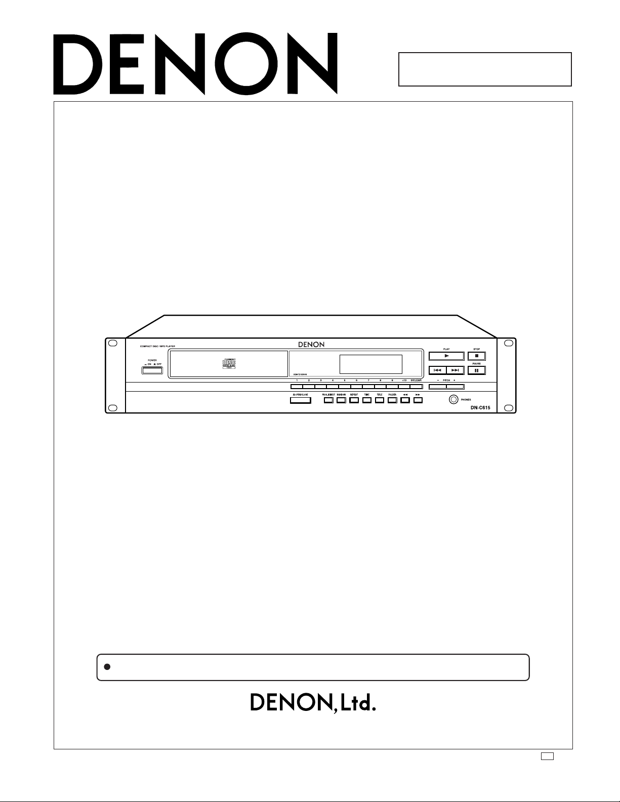
DN-C615
SERVICE MANUAL
MODEL
DN-C615
STEREO CD/MP3 PLAYER
Some illustrations using in this service manual are slightly different from the actual set.
16-11, YUSHIMA 3-CHOME, BUNKYOU-KU, TOKYO 113-0034 JAPAN
Telephone: 03 (3837) 5321
X0160 NC 0211
For U.S.A., Canada, Europe,
Korea model

2
2
DN-C615
CD SECTION
Typ e: Single-mechanism compact disc player
Audio channel: 2 channel stereo
Quantization: 16-bit Liner
Sampling Frequency: 44.1kHz at Normal Pitch
Oversampling Ratio: 8 times
Frequency Response: 20 to 20,000Hz
Total Harmonic Distortion: 0.007%
Signal-to-noise Ratio: 107dB
Dynamic Range: 98dB
Channel Separation: 90dB
Analog Output: RCA jack
Output Level: 2.0 V at 0 dB disc
Load Impedance: 10kΩ/kohms or more
Digital Output: RCA jack
Signal Format: SPDIF or IEC-958 Type II
Variable Pitch Control: 12% max.
Frame Search Accuracy: 1/75 second
Discs: Standard compact discs (12cm and 8 cm)
CD Mechanism Service Life: 1000 hours (continuous playback)
REMOTE Wired Remote Control Connection (Stereo mini jack)
Remote Control Sensor
GENERAL
Headphone Output: Stereo
Outputs Level: 410mW
Load Impedance: 33Ω/ohms
Power supply: 120V AC 10%,60Hz (for U.S.A & Canada models)
230V AC 10%,50Hz (for European & U.K. models)
Power Consumption: 13W
Dimensions: 482 (W) x 88 (H) x 280 (D) mm
Installation: 19-inch rack mountable (2U)
Mass: 4.7kg
*For improvement purposes,specifications and design are subject to change without notice.
SPECIFICATIONS
SAFETY PRECAUTIONS
The following check should be performed for the continued protection of the customer and service technician.
LEAKAGE CURRENT CHECK
Before returning the unit to the customer, make sure you make either (1) a leakage current check or (2) a line to chassis
resistance check. If the leakage current exceeds 0.5 milliamps, or if the resistance from chassis to either side of the
power cord is less than 460 kohms, the unit is defective.
3
3
DN-C615
DISASSEMBLY
(To reassemble, reverse disassembly)
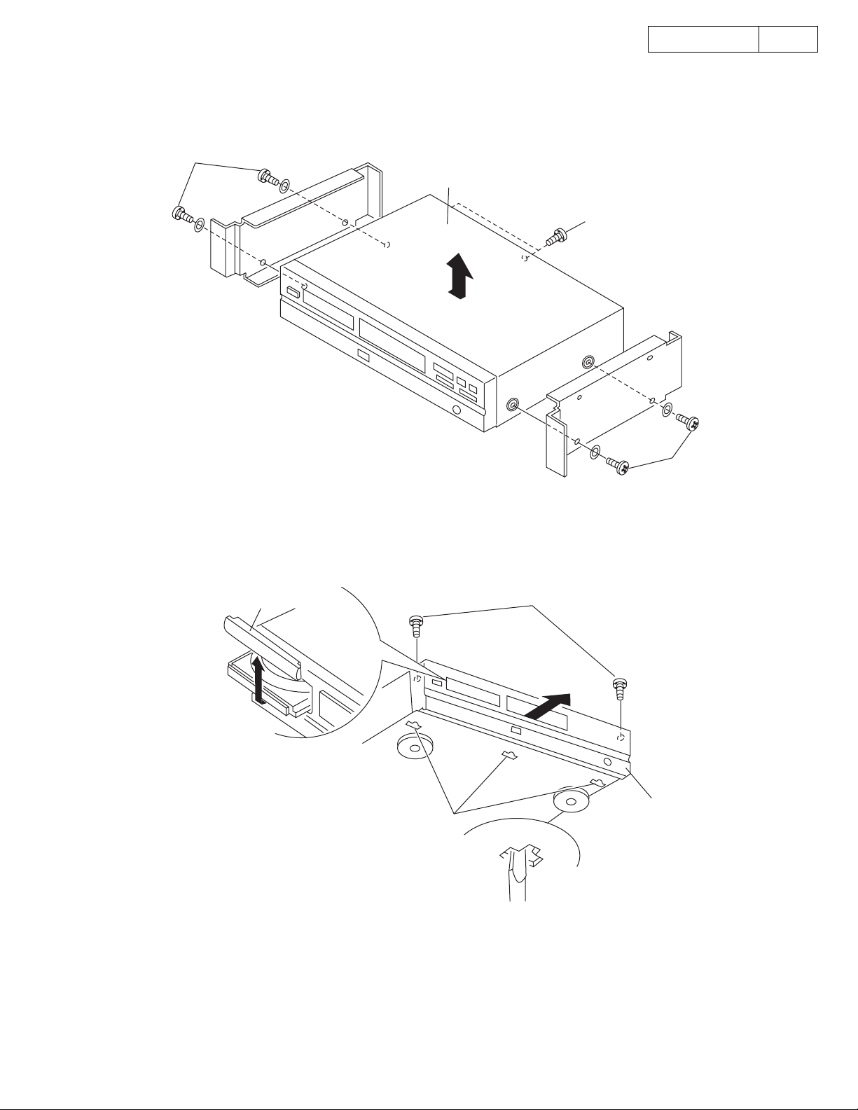
1. TOP COVER
(1) Remove 4screws from both sides and 2 screws from back Panel.
2. FRONT PANEL
(1) Pull Loader frame frontward, and remove loader panel.
(2) Remove 2 front panel upper screws.
(3) Undo 2 front panel upper hooks.
(4) Pull front panel and undo 3 lower hooks.
Screw
Screw
Screw
Top cover
Loader Panel
Screw
Hook
Front panel
4
4
DN-C615
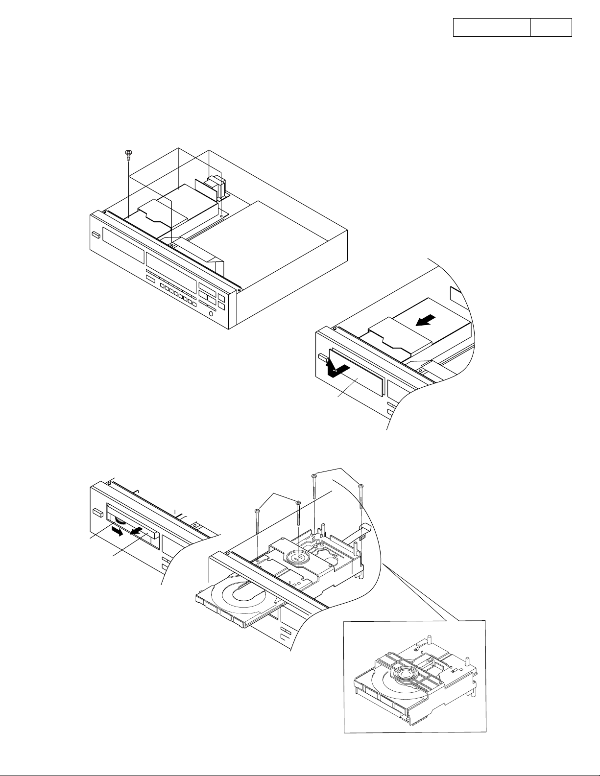
3. MECHANISM UNIT
3.1. How to remove a mechanism unit in case a power supply is not turned on.
(1) Remove 4 screws on the Mecha base.
(2) Remove the CD Mecha to the arrow direction.
(3) Detach the Loader panel to the arrow direction.
(4) A gear is turned and a tray is turned in the direction of an arrow.
(5) A tray is pinched and it turns in the direction of an arrow.
(6) Remove 4 screws on the Mechanism unit
Loader panel
Gear
Tray
Screw
Screw
5
5
DN-C615
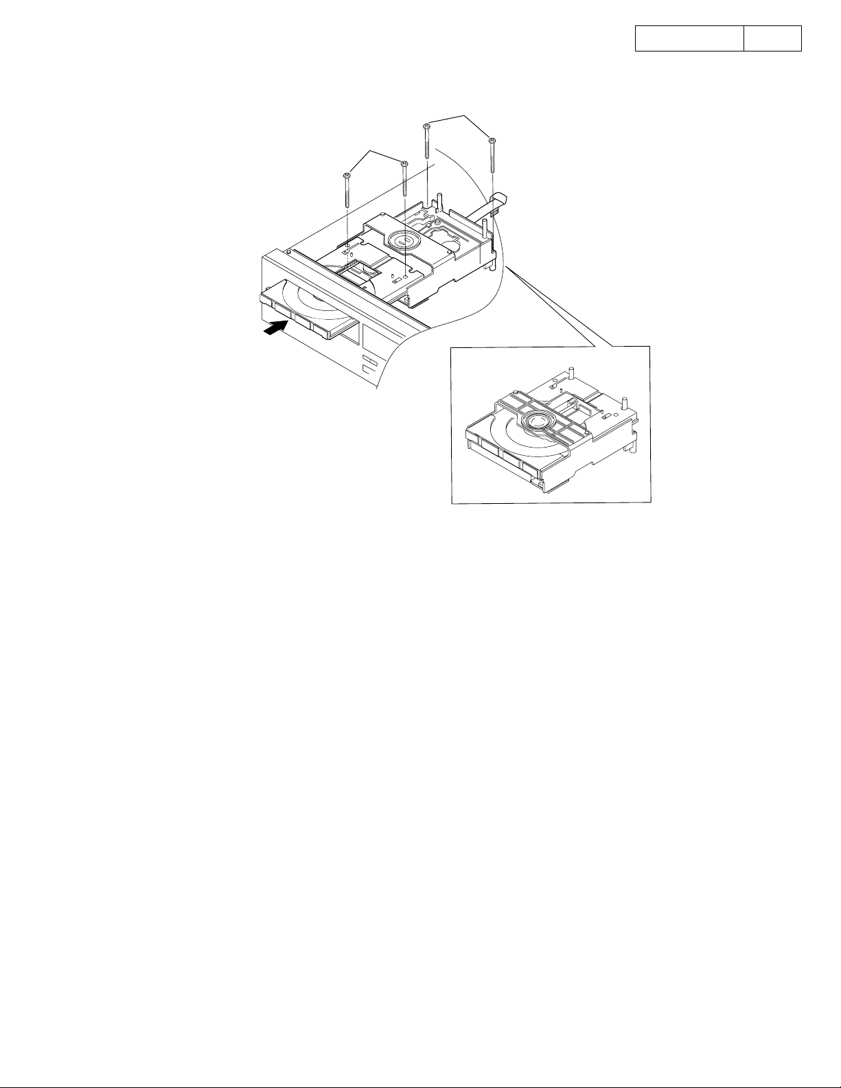
3.2. How to remove a mechanism unit in case a power supply is turned on.
(1) Remove 4 screws.
Screw
Screw
6
6
DN-C615
SERVICE PROGRAM
1. REQUIRED MEASURING IMPLEMENT
• Reference disc (TCD784 or CO-74176)
1.1. What is Service Program
Service program is a special program intended for confirming servo functions etc.
1.2. µcom Version Check
• Refer to "Preset Functions and Operations" of the instruction manual.
• You can check the
µ
com version.
1.3. B.E.R. Checks and Automatic Servo Adjustment Call
• Switch on the power while pushing the 5 button and 6 button at the same time. And Loading a disc
by OPEN/CLOSE button.
(1) Block Error Rate
Press the PLAY button. B.E.R. is displayed.
01Tr **m XXXX XXXX: Block Error Rate
You can select the track by the 、 button.
(2) Tracking balance and Focus balance data
Press the 2 button. Tracking balance and Focus balance data is displayed.
2
±
XXX
±
@@@ XXX: Tracking balance
@@@: Focus balance
(3) Focus gain data
Press the 3 button. Focus gain data is displayed.
3 XXXX XXXX: Focus gain
(4) Tracking gain data
Press the 4 button. Tracking gain data is displayed.
4 XXXX XXXX: Tracking gain
(5) Tracking offset and Focus offset data
Press the 5 button. Tracking offset and Focus offset data is displayed.
5
±
XXX
±
@@@ XXX: Tracking offset
@@@: Focus offset
(6) Press the 1 button to select the Block Error Rate data.
(7) To stop the B.E.R. Check and Automatic Servo Adjustment Call mode, please turn off the POWER switch.
Adjustment Item Adjustment Value indicator
1 Tracking Balance -025 ~ +025
2 Focus Balance -030 ~ +030
3 Focus Gain 0576 ~ 2304
4 Tracking Gain 0392 ~ 1569
5 Tracking Offset -005 ~ +005
6 Focus Offset -005 ~ +005
7
7
DN-C615
1.4. Test Mode (Heat Run mode)
• Switch on the power while pushing the 3 button and 4 button at the same time. "000TroHR0000" is
displayed. And the tray is opened
(1) Hold the disc by the edges and place it on the disc tray.
(2) Starting with the OPEN/CLOSE button, it repeats open/close of the tray and playback.
***TrxHRXXXX ***: Track No.
x : o, c, s, t, r, and p
XXXX: Cycle quantity
All tracks are played back if the track count is less than 20. Only the first and last tracks are played
back if the tracks are more than 21. When any errors, it stops and indicates error code
(Refer to the Error Code Table).
(3) To stop the Test mode, please turn off the POWER switch.
1.5. Error Code Table
Error Code CONTENTS
Error 01 Unable to close the loader tray in the regulation time.
Error 02 Unable to open the loader tray in the regulation time.
Error 03 Inner circle switch ON error even if the time is over.
Error 04 Inner circle switch OFF error even if the time is over.
Error 05 The focus offset adjustment result is outside the regulation range.
Error 06 Unable to adjust the focus offset in the regulation time.
Error 07 The tracking offset adjustment result is outside the regulation range.
Error 08 Unable to adjust the tracking offset in the regulation time
Error 09 The FE peak is outside the regulation range.
Error 0A The FE peak is outside the regulation range.
Error 0B Unable to adjust the focus rough gain in the regulation time.
Error 0C The focus rough gain is outside the regulation range.
Error 0D Unable to actuate focus in the regulation time.
Error 0E Unable to actuate tracking in the regulation time.
Error 0F Unable to adjust the tracking rough gain in the regulation time.
Error 10 The tracking rough gain is outside the regulation range.
Error 11 Unable to adjust the tracking balance in the regulation time.
Error 12 The tracking balance adjustment result is outside the regulation range.
Error 13 Focus servo down during automatic adjustment.
Error 14 Focus servo down during automatic adjustment.
Error 15 Unable to adjust the focus balance in the regulation time.
Error 16 The focus balance adjustment result is outside the regulation range.
Error 17 Track servo down during automatic adjustment.
Error 18 Unable to adjust the focus fine gain in the regulation time.
8
8
DN-C615
2. µCOM VERSION UPGRADE
System µcom can be upgraded in the following manner.
Version Upgrade Method
(1) Record the version upgrade software on a CD-R or CD-RW disc, only as one file with the format ISO9660 Mode-1. The file
name of the supplied version upgrade software should be used as is and this disc needs to finalize.
(2) Hold the disc by the edges and place it on the disc tray.
(3) Press the OPEN/CLOSE button to start the version upgrade.
"Version Up" "Push Play!" "xxxx->XXXX" are displayed.
xxxx : current version
XXXX : upgrade version
(4) Press the PLAY button.
"Now Writing" "Writing-XXX" are displayed.
XXX : count up from 000 to129
(5) When the version upgrade is finished, "Complete!" is indicated.
(6) Turn off the power once and turn on ag ain. Press the OPEN/CLOSE button and remove the disc.
NOTE:
When the power is turned off before “Complete!” is displayed, µcon version is not written correctly.
Error Code CONTENTS
Error 19 The focus fine gain is outside the regulation range.
Error 1A Unable to adjust the tracking fine gain in the regulation time.
Error 1B The tracking fine gain is outside the regulation range.
Error 1C Unable to adjust automatically in the regulation time.
Error 1D Unable to read the subcode Q in the regulation time.
Error 1E Unable to read the TOC in the regulation time.
Error 1F Focus servo down during search (over the regulation time).
Error 20 Track servo down during search (over the regulation time).
Error 2116 Servo error during search.
Error 2103 Search error (over the regulation time).
Error 22 Discontinuity occurred, during write to the DRAM.
Error 23 The error which cannot be corrected to the read data.
Error 24 Unable to do the level detect.
Error 25 Unable to join data in the regulation time.
Error 26 The error rate when recording on the memory is over the regulation value.
Error 27 The subcode jump more than regulation.
9
9
DN-C615
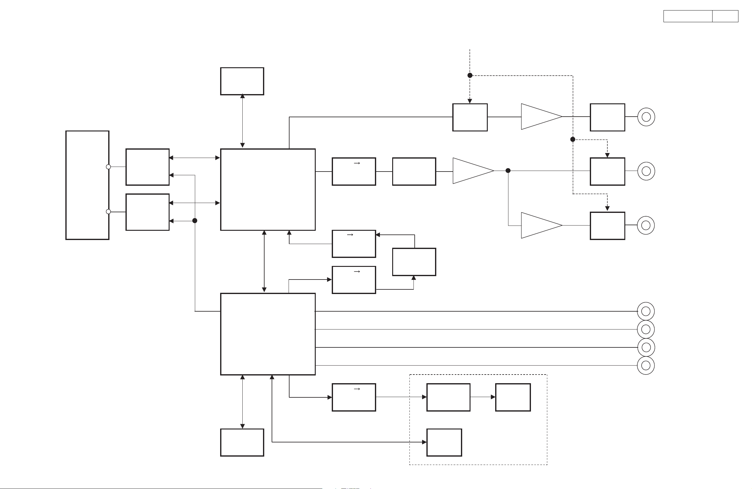
BLOCK DIAGRAM
SN74LV244
3.3V
5V
I/F
TC74HCT7007
4M FLASH
ROM
KEY
FLD
DRIVER
M66005FP
3.3V
5V
I/F
TC74HCT7007
16M DRAM
P. TRANS
MUTE
FLD
CLOCK GEN
SYSTEM uCOM
MN102H60KDA
3.3V
5V
I/F
TC74HCT7007
5V
3.3V
I/F
MUTE
MUTE
DSP
MN662791
AN22002A
DAC
PCM1716E
CD MECHA
MOTOR
ACTUATOR
P.U
DRIVER
AN8785SB
HEAD AMP
<CD MUTE>
WIRED
REMOTE
IN
RC5
OUT
EXT
H/P OUT
CD OUT
DIGITAL
OUT
10
10
DN-C615
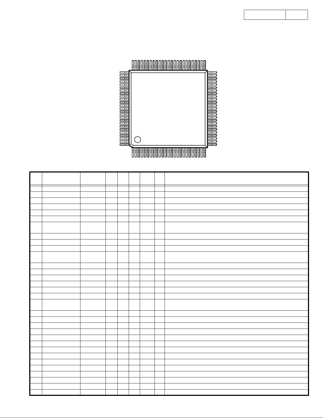
SEMICONDUCTORS
IC’s
MN102H60KDA
(IC101)
MN102H60KDA Terminal Function
Pin
No.
Pin Name Symbol I/O Det Ext Res Ini Function
1 P60, WAIT, SBT2 PCDMUTE O - Pd L L Mute for CD
2 P61, _RE _RD O - - Hi-Z - Read signal
3 P62, _WEL _WEL O - - Hi-Z - Write signal
4 P63, _WE, _WEH PEXTIN I - - Hi-Z - EXT.IN signal
5 _CS0,TM13OA _CS0 O - - Hi-Z - Chip select signal (MASK ROM operation : Input port)
6 _CS1, TM13OB _CS1 O - - Hi-Z - Chip select signal (IN/OUT)
7 _CS2, TM14OA _CS2 O - - Hi-Z - Chip select signal (Normal operation : Input port, MASK ROM operation
: F.ROM Chip select)
8 _CS3, TM14OB _CS3 O - - Hi-Z - Deck (Input/Output)
9 P54, _BREQ PEXTOUT O - - Hi-Z H EXT.OUT signal
10 P55, _BRACK PRMTOUT O - - Hi-Z H Remote output signal
11 P56, ALE, _ALE,
_BSTRE, TM15IA
PMON2 I - - Hi-Z - Monitor signal 2
12 P57,_WORD _WORD I - H H H Data bit bus width select 'H': 8bit
13 P20,A00,SBT2 A00 A/O - - Unfix - Address bus
14 P21,A01,SBI2 A01 A/O - - Unfix - Address bus
15 P22,A02,SBO2 A02 A/O - - Unfix - Address bus
16 P23,A03 A03 A/O - - Unfix - Address bus
17 Vdd Vdd - - - - - Power supply (+3.3V)
18 BOSC,BIBT1,
BIBT2,PB0
PIRINH O - - Hi-Z L Infrared remote 'L': Enable / 'H': Inhibit
19 Vss Vss - - - - - GND(0V)
20 XI,PB1 PCE O - - Hi-Z L Chip select 'L': MN662791 / 'H': BU2618
21 XO XO - - - - - Not used. OPEN
22 Vdd Vdd - - - - - Power supply (+3.3V)
23 OSCI OSCI I - - - -
24 OSCO OSCO O - - - - OSCI output
25 MODE MODE I - L L L Mode select 'L': Processor mode
26 P24,A04,TM15IA A04 A/O - - Unfix - Address bus
27 P25,A05 A05 A/O - - Unfix - Address bus
28 P26,A06 A06 A/O - - Unfix - Address bus
29 P27,A07 A07 A/O - - Unfix - Address bus
30 P30,A08,_KI0 A08 A/O - - Unfix - Address bus
31 P31,A09,_KI1 A09 A/O - - Unfix - Address bus
32 P32,A10,_KI2 A10 A/O - - Unfix - Address bus
75
76
100
1
25
26
50
51
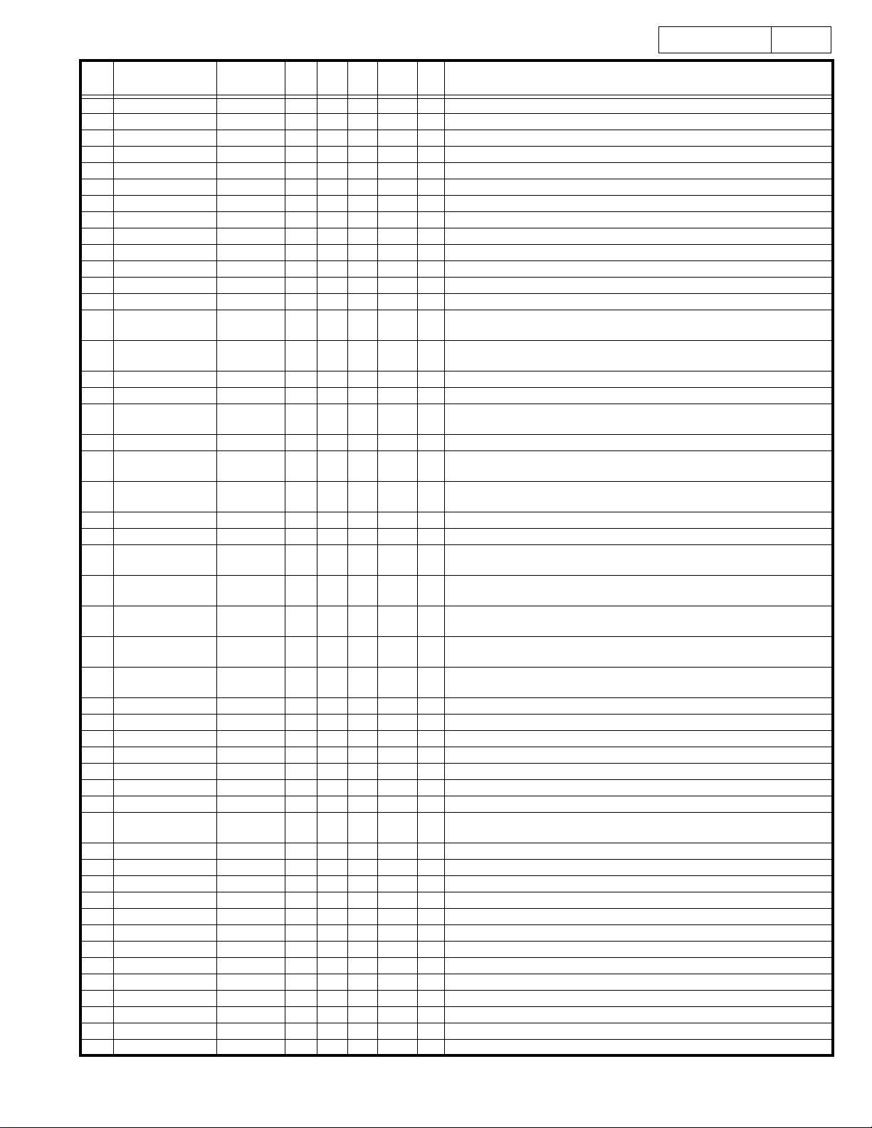
11
11
DN-C615
33 P33,A11,_KI3 A11 A/O - - Unfix - Address bus
34 AVDD AVDD - - - - - Analog power supply terminal
35 P34,A12,_KI4 A12 A/O - - Unfix - Address bus
36 P35,A13,_KI5 A13 A/O - - Unfix - Address bus
37 P36,A14,_KI6 A14 A/O - - Unfix - Address bus
38 P37,A15,_KI7 A15 A/O - - Unfix - Address bus
39 P40,A16 A16 A/O - - Unfix - Address bus
40 P41,A17 A17 A/O - - Unfix - Address bus
41 P42,A18 A18 A/O - - Unfix - Address bus
42 P43,A19 A19 A/O - - Unfix - Address bus
43 Vref- Vref- - - - - - Standard analog power supply
44 P44,AN4,A20 PPARA1 I Lv - Unfix - Parallel input 1 (Use A/D converter)
45 P45,AN5,A21 PPARA2 I Lv - Unfix - Parallel input 2 (Use A/D converter)
46 P46,AN6,STOP,
A22
PPARA3 I Lv - Hi-Z - Parallel input 3 (Use A/D converter)
47 P47,AN7,WDOUT,
A23
PSDA I/O - - Hi-Z - Not used.
48 P80,TM14OA PSCL O - - Hi-Z H Not used.
49 P81,TM14OB PDUB O - - Hi-Z H Dubbing signal 'L': Dubbing
50 P82,TM0IO,SBI2,
SBT3,SCL3
PMON1 I - - Hi-Z - Monitor signal 1
51 P83,TM4IO,SBI3 RxD I - - Hi-Z - Serial port (9600bps by xxMHz)
52 P84,TM7IO,SBO3,
SDA3
TxD O - - Hi-Z H Serial port (9600bps by xxMHz)
53 P85,TM9IOA,SBO2,
SBT4,SCL4
PFLCLK O - - Hi-Z H To FL driver SCK
54 Vref+ Vref+ - - - - - Standard analog power supply
55 P86,TM9IOB,SBI4 PFLCS O - - Hi-Z H To FL driver CS
56 P87,TM9IC,SBO4,
SDA4
PFLSD O - - Hi-Z H To FL driver SDATA
57 P90,TM8IOA,BIBT1,
_DMAREQ1
PBIAS O - Pd L L Bias signal 'H': BIAS ON
58 P91,TM10IOA,BIBT2,
_DMAACK1
PRMUTE O - Pu H H Rec mute change signal 'H': MUTE ON
59 P92,TM10IOB,
_DMAREQ0
PLRCK I Ed - Hi-Z - LRCK : Use for time code creation during MP3 playback.
60 P93,TM10IC,
_DMAACK0
PNRST O - Pd L L Round IC reset signal
61 Vss Vss - - - - - GND (0V)
62 P94,AN0 PADINL I Lv Pd L - Use A/D converter
63 P95,AN1 PADINR I Lv Pd L - Use A/D converter
64 P96,AN2 PREMO1 I Lv - Hi-Z - Use A/D converter
65 P97,AN3 PREMO2 I Lv - Hi-Z - Use A/D converter
66 Vdd Vdd - - - - - Power supply (+3.3V)
67 P70,SBT0,_RAS PMCLK O - - Hi-Z H DSP interface Clock (clock synchronous formula)
68 P71,SBI0,_CAS,
_LCAS
PSTAT I - - Hi-Z - DSP interface Reception (clock synchronous formula)
69 P72,SBO0,_UCAS PMDAT O - - Hi-Z H DSP interface Transmission (clock synchronous formula)
70 P73,SBT1,DUMX PTXTCLK O - - Hi-Z H Use during CD-TEXT data read (clock synchronous formula)
71 P74,SBI1 PTXTD I - - Hi-Z - Use during CD-TEXT data read (clock synchronous formula)
72 P75,SBO1 PMLD O - - Hi-Z H DSP interface latch
73 TEST1 TEST1 I - Pu - - Pull up 33 - 50K
74 TEST2 TEST2 I - Pu - - Pull up 33 - 50K
75 _NMI _NMI I Lv - Hi-Z - Need pull up
76 PA0,_IRQ0 PBLKCK I Ed - Hi-Z - Sub code clock interruption
77 PA1,_IRQ1 PDQSY I Ed - Hi-Z - CD-TEXT DQSY Interruption
78 PA2,_IRQ2 PPLS I Ed - Hi-Z - Count by DOWN EDGE. One rotation by three counts.
79 PA3,_IRQ3 PREMOTE I Ed - Hi-Z - RC-5/Infrared remote signal input
80 PA4,_IRQ4,TM15IB PCHGOFT O - Pu H L Off track signal
81 PA5,ADSEP ADSEP I - H H H 'H': Address data separation mode / 'L': Address data common mode
Pin
No.
Pin Name Symbol I/O Det Ext Res Ini Function
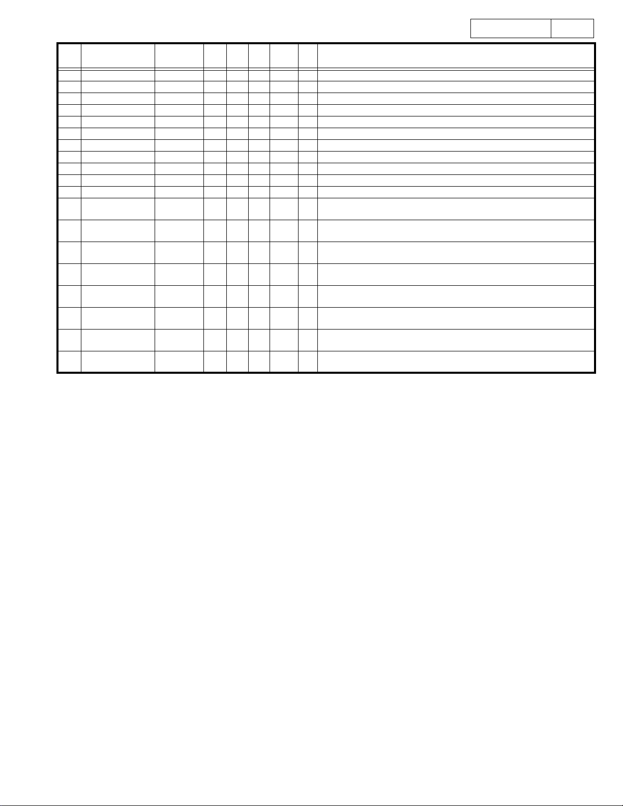
12
12
DN-C615
82 _RST _RESET I Lv - L - Reset signal 'L': RESET
83 Vdd Vdd - - - - - Power supply (+3.3V)
84 P00,D00,AD00 D00 D/O - - Hi-Z - Data bus
85 P01,D01,AD01 D01 D/O - - Hi-Z - Data bus
86 P02,D02,AD02 D02 D/O - - Hi-Z - Data bus
87 P03,D03,AD03 D03 D/O - - Hi-Z - Data bus
88 P04,D04,AD04 D04 D/O - - Hi-Z - Data bus
89 P05,D05,AD05 D05 D/O - - Hi-Z - Data bus
90 P06,D06,AD06 D06 D/O - - Hi-Z - Data bus
91 P07,D07,AD07 D07 D/O - - Hi-Z - Data bus
92 Vss Vss - - - - - GND(0V)
93 P010,D08,AD08,
TM8IOB
PMIX O - Pd L L Deck line out 'H': Mix out of CD+DECK
94 P011,D09,AD09,
TM8IC
PPOFF I - - H - 'L': Power failure detection
95 P012,D10,AD10,
TM11IOA
PDECKM
UT
O - Pd L L Deck line mute 'L': MUTE ON
96 P013,D11,AD11,
TM11IOB
POPEN I - - Hi-Z - OPEN switch
97 P014,D12,AD12,
TM11IC
PCLOSE I - - Hi-Z - CLOSE switch
98 P015,D13,AD13,
TM12IOA
PLOAD O - - Hi-Z H OPEN/CLOSE signal (PWM out put) (During Pnrst='L', out put
PWM(50%))
99 P016,D14,AD14,
TM12IOB
O--Hi-ZH
100 P017,D15,AD15,
TM12IC
PINSW I - - Hi-Z - Inner circle SW
Pin
No.
Pin Name Symbol I/O Det Ext Res Ini Function
 Loading...