


AMD Advanced Micro Devices AM29LV001BT-90FI, AM29LV001BT-90FEB, AM29LV001BT-90FE, AM29LV001BT-90FCB, AM29LV001BT-90FC Datasheet
...PRELIMINARY
Am29LV001B
1 Megabit (128 K x 8-Bit)
CMOS 3.0 Volt-only Boot Sector Flash Memory
DISTINCTIVE CHARACTERISTICS
■ Single power supply operation |
■ Unlock Bypass Mode Program Command |
—Full voltage range: 2.7 to 3.6 volt read and write operations for battery-powered applications
—Regulated voltage range: 3.0 to 3.6 volt read and write operations and for compatibility with high performance 3.3 volt microprocessors
■Manufactured on 0.35 µm process technology
■High performance
—Full voltage range: access times as fast as 55 ns
—Regulated voltage range: access times as fast as 45 ns
■Ultra low power consumption (typical values at 5 MHz)
—200 nA Automatic Sleep mode current
—200 nA standby mode current
—7 mA read current
—15 mA program/erase current
■Flexible sector architecture
—One 8 Kbyte, two 4 Kbyte, and seven 16 Kbyte
—Supports full chip erase
—Sector Protection features:
Hardware method of locking a sector to prevent any program or erase operations within that sector
Sectors can be locked in-system or via programming equipment
Temporary Sector Unprotect feature allows code changes in previously locked sectors
—Reduces overall programming time when issuing multiple program command sequences
■Top or bottom boot block configurations available
■Embedded Algorithms
—Embedded Erase algorithm automatically preprograms and erases the entire chip or any combination of designated sectors
—Embedded Program algorithm automatically writes and verifies data at specified addresses
■Minimum 1,000,000 write cycle guarantee per sector
■Package option
—32-pin TSOP
—32-pin PLCC
■Compatibility with JEDEC standards
—Pinout and software compatible with singlepower supply Flash
—Superior inadvertent write protection
■Data# Polling and toggle bits
—Provides a software method of detecting program or erase operation completion
■Erase Suspend/Erase Resume
—Supports reading data from or programming data to a sector that is not being erased
■Hardware reset pin (RESET#)
—Hardware method for resetting the device to reading array data
Publication# 21557 Rev: C Amendment/0
Issue Date: April 1998

P R E L I M I N A R Y
GENERAL DESCRIPTION
The Am29LV001B is a 1 Mbit, 3.0 Volt-only Flash memory device organized as 131,072 bytes. The Am29LV001B has a boot sector architecture.
The device is offered in 32-pin PLCC and 32-pin TSOP packages. The byte-wide (x8) data appears on DQ7– DQ0. All read, erase, and program operations are accomplished using only a single power supply. The device can also be programmed in standard EPROM programmers.
The standard Am29LV001B offers access times of 45, 55, 70, and 90 ns, allowing high speed microprocessors to operate without wait states. To eliminate bus contention, the device has separate chip enable (CE#), write enable (WE#) and output enable (OE#) controls.
The device requires only a single power supply (2.7 V–3.6V) for both read and write functions. Internally generated and regulated voltages are provided for the program and erase operations.
The Am29LV001B is entirely command set compatible with the JEDEC sin gle - pow er-sup ply Flash standard. Commands are written to the command register using standard microprocessor write timings. Register contents serve as input to an internal statemachine that controls the erase and programming circuitry. Write cycles also internally latch addresses and data needed for the programming and erase operations. Reading data out of the device is similar to reading from other Flash or EPROM devices.
Device programming occurs by executing the program command sequence. This initiates the Embedded Program algorithm—an internal algorithm that automatically times the program pulse widths and verifies proper cell margin. The Unlock Bypass mode facilitates faster programming times by requiring only two write cycles to program data instead of four.
Device erasure occurs by executing the erase command sequence. This initiates the Embedded Erase algorithm—an internal algorithm that automatically preprograms the array (if it is not already programmed) before executing the erase operation. During erase, the
device automatically times the erase pulse widths and verifies proper cell margin.
The host system can detect whether a program or erase operation is complete by reading the DQ7 (Data# Polling) and DQ6 (toggle) status bits. After a program or erase cycle has been completed, the device is ready to read array data or accept another command.
The sector erase architecture allows memory sectors to be erased and reprogrammed without affecting the data contents of other sectors. The device is fully erased when shipped from the factory.
Hardware data protection measures include a low VCC detector that automatically inhibits write operations during power transitions. The hardware sector protection feature disables both program and erase operations in any combination of the sectors of memory. This can be achieved in-system or via programming equipment.
The Erase Suspend feature enables the user to put erase on hold for any period of time to read data from, or program data to, any sector that is not selected for erasure. True background erase can thus be achieved.
The hardware RESET# pin terminates any operation in progress and resets the internal state machine to reading array data. The RESET# pin may be tied to the system reset circuitry. A system reset would thus also reset the device, enabling the system microprocessor to read the boot-up firmware from the Flash memory.
The device offers two power-saving features. When addresses have been stable for a specified amount of time, the device enters the automatic sleep mode. The system can also place the device into the standby mode. Power consumption is greatly reduced in both these modes.
AMD’s Flash technology combines years of Flash memory manufacturing experience to produce the highest levels of quality, reliability and cost effectiveness. The device electrically erases all bits within a sector simultaneously via Fowler-Nordheim tunneling. The data is programmed using hot electron injection.
Am29LV001B |
2 |
P R E L I M I N A R Y
PRODUCT SELECTOR GUIDE
Family Part Number |
|
Am29LV001B |
|
||
|
|
|
|
|
|
Speed Options |
Regulated Voltage Range: VCC =3.0–3.6 V |
-45R |
|
|
|
|
|
|
|
|
|
Full Voltage Range: VCC = 2.7–3.6 V |
|
-55 |
-70 |
-90 |
|
|
|
||||
|
|
|
|
|
|
Max access time, ns (tACC) |
45 |
55 |
70 |
90 |
|
|
|
|
|
|
|
Max CE# access time, ns (tCE) |
45 |
55 |
70 |
90 |
|
|
|
|
|
|
|
Max OE# access time, ns (tOE) |
25 |
30 |
30 |
35 |
|
|
|
|
|
|
|
Note: See “AC Characteristics” for full specifications.
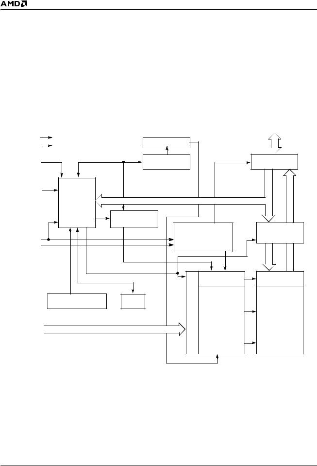
BLOCK DIAGRAM
|
|
|
|
|
|
DQ0–DQ7 |
VCC |
|
Sector Switches |
|
|
|
|
VSS |
|
|
|
|
|
|
|
|
|
|
|
|
|
RESET# |
|
Erase Voltage |
|
|
|
Input/Output |
|
Generator |
|
|
|
Buffers |
|
|
|
|
|
|
||
WE# |
State |
|
|
|
|
|
|
Control |
|
|
|
|
|
|
Command |
|
|
|
|
|
|
Register |
PGM Voltage |
|
|
|
|
|
|
Generator |
|
|
|
|
|
|
|
Chip Enable |
STB |
Data |
|
|
|
|
Latch |
|||
CE# |
|
Output Enable |
||||
|
|
|
||||
OE# |
|
|
|
Logic |
|
|
|
|
|
|
|
|
|
|
|
STB |
|
Y-Decoder |
|
Y-Gating |
|
|
|
|
|
|
|
|
VCC Detector |
Timer |
Latch |
|
|
|
|
|
|
|
|
|
|
|
|
|
Address |
X-Decoder |
|
Cell Matrix |
A0–A16 |
|
|
|
|
|
|
|
|
|
|
|
|
|
|
|
|
|
|
|
21557C-1 |
3 |
Am29LV001B |
P R E L I M I N A R Y
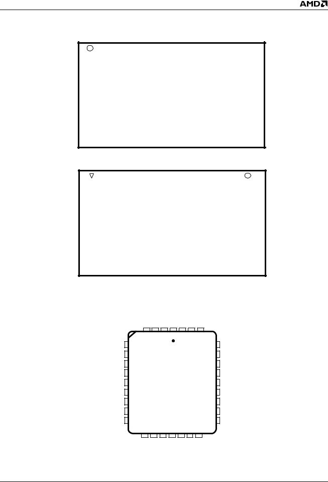
CONNECTION DIAGRAMS
A11  1
1
A9  2
2
A8  3
3
A13  4
4
A14  5
5
NC  6
6
WE#  7
7
VCC  8
8
RESET#  9
9
A16  10
10
A15  11
11
A12  12
12
A7  13
13
A6  14
14
A5  15
15
A4  16
16
OE#  1
1
A10  2
2
CE#  3
3
DQ7  4
4
DQ6  5
5
DQ5  6
6
DQ4  7
7
DQ3  8
8
VSS  9
9
DQ2  10
10
DQ1  11
11
DQ0  12
12
A0  13
13
A1  14
14
A2  15
15
A3  16
16
32-Pin Standard TSOP
32-Pin Reverse TSOP
32  OE#
OE#
31  A10
A10
30  CE#
CE#
29  DQ7
DQ7
28  DQ6
DQ6
27  DQ5
DQ5
26  DQ4
DQ4
25  DQ3
DQ3
24  VSS
VSS
23  DQ2
DQ2
22  DQ1
DQ1
21  DQ0
DQ0
20  A0
A0
19  A1
A1
18  A2
A2
17  A3
A3
32  A11
A11
31  A9
A9
30  A8
A8
29  A13
A13
28  A14
A14
27  NC
NC
26  WE#
WE#
25  VCC
VCC
24  RESET#
23  A16
A16
22  A15
A15
21  A12
A12
20  A7
A7
19  A6
A6
18  A5
A5
17  A4
A4
|
|
|
|
A12 |
A15 |
A16 |
RESET# |
V WE# |
NC |
|
||||||||
|
|
|
|
|
|
|
|
|
|
|
|
|
CC |
|
|
|||
|
|
|
|
|
3 |
2 |
1 |
32 31 30 |
|
|||||||||
|
|
|
4 |
|
||||||||||||||
A7 |
5 |
|
|
|
|
|
|
|
|
|
|
|
|
|
|
29 |
A14 |
|
A6 |
6 |
|
|
|
|
|
|
|
|
|
|
|
|
|
|
28 |
A13 |
|
A5 |
7 |
|
|
|
|
|
|
|
|
|
|
|
|
|
|
27 |
A8 |
|
A4 |
8 |
|
|
|
|
|
|
|
|
|
|
|
|
|
|
26 |
A9 |
|
|
|
|
|
|
|
|
|
|
|
|
|
|
||||||
A3 |
9 |
|
|
|
|
|
|
PLCC |
25 |
A11 |
||||||||
|
|
|
|
Am29LV001 |
|
|||||||||||||
A2 |
10 |
|
|
|
|
|
|
|
|
|
|
|
|
|
24 |
OE# |
||
|
|
|
|
|
|
|
|
|
|
|
|
|
||||||
A1 |
11 |
|
|
|
|
|
|
|
|
|
|
|
|
|
23 |
A10 |
||
A0 |
12 |
|
|
|
|
|
|
|
|
|
|
|
|
|
22 |
CE# |
||
DQ0 |
13 |
|
|
|
|
|
|
|
|
|
|
|
|
|
21 |
DQ7 |
||
|
14 15 16 17 18 19 20 |
|
||||||||||||||||
|
|
|
|
|
|
|
|
|
|
|
|
|
|
|
|
|
|
|
|
|
|
|
DQ1 |
DQ2 |
SS |
DQ3 |
DQ4 DQ5 |
DQ6 |
|
||||||||
|
|
|
|
V |
|
|||||||||||||
|
|
|
|
|
|
|
|
|
|
|
|
|
|
|
|
|
|
21557C-2 |
Am29LV001B |
4 |
P R E L I M I N A R Y
PIN CONFIGURATION
A0–A16 |
= |
17 addresses |
DQ0–DQ7 |
= |
8 data inputs/outputs |
CE# |
= |
Chip enable |
OE# |
= |
Output enable |
WE# |
= |
Write enable |
RESET# |
= Hardware reset pin, active low |
|
VCC |
= 3.0 volt-only single power supply |
|
|
|
(see Product Selector Guide for speed |
|
|
options and voltage supply tolerances) |
VSS |
= |
Device ground |
NC |
= Pin not connected internally |
|
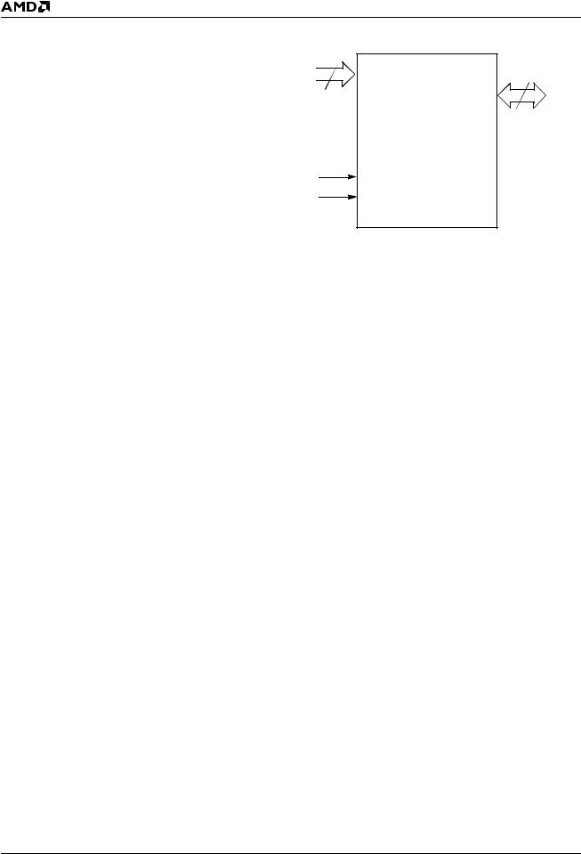
LOGIC SYMBOL
17 |
|
A0–A16 |
8 |
DQ0–DQ7
 CE#
CE#
 OE#
OE#
WE#
RESET#
21557C-3
5 |
Am29LV001B |
P R E L I M I N A R Y
ORDERING INFORMATION
Standard Products
AMD standard products are available in several packages and operating ranges. The order number (Valid Combination) is formed by a combination of the elements below.
Am29LV001B |
T |
-45R |
E |
C |
OPTIONAL PROCESSING
Blank = Standard Processing
B = Burn-in
(Contact an AMD representative for more information)
TEMPERATURE RANGE
C = Commercial (0°C to +70°C)
I |
= Industrial (–40°C to +85°C) |
E = Extended (–55°C to +125°C) |
|
PACKAGE TYPE |
|
E |
= 32-Pin Thin Small Outline Package (TSOP) |
|
Standard Pinout (TS 032) |
F |
= 32-Pin Thin Small Outline Package (TSOP) |
|
Reverse Pinout (TSR032) |
J |
= 32-Pin Rectangular Plastic Leaded Chip |
|
Carrier (PL 032) |
SPEED OPTION
See Product Selector Guide and Valid Combinations
BOOT CODE SECTOR ARCHITECTURE
T = Top Sector
B = Bottom Sector
DEVICE NUMBER/DESCRIPTION
Am29LV001B
1 Megabit (128 K x 8-Bit) CMOS Flash Memory
3.0 Volt-only Read, Program, and Erase
Valid Combinations
Am29LV001BT-45R,
EC, FC, JC
Am29LV001BB-45R,
Am29LV001BT-55,
Am29LV001BB-55,
Am29LV001BT-70,
EC, EI, EE,
Am29LV001BB-70,
FC, FI, FE,
JC, JI, JE
Am29LV001BT-90,
Am29LV001BB-90,
Valid Combinations
Valid Combinations list configurations planned to be supported in volume for this device. Consult the local AMD sales office to confirm availability of specific valid combinations and to check on newly released combinations.
Am29LV001B |
6 |

P R E L I M I N A R Y
DEVICE BUS OPERATIONS
This section describes the requirements and use of the device bus operations, which are initiated through the internal command register. The command register itself does not occupy any addressable memory location. The register is composed of latches that store the commands, along with the address and data information needed to execute the command. The contents of
the register serve as inputs to the internal state machine. The state machine outputs dictate the function of the device. Table 1 lists the device bus operations, the inputs and control levels they require, and the resulting output. The following subsections describe each of these operations in further detail.
Table 1. Am29LV001B Device Bus Operations
Operation |
CE# |
OE# |
WE# |
RESET# |
Addresses (Note 1) |
DQ0–DQ7 |
|
|
|
|
|
|
|
Read |
L |
L |
H |
H |
AIN |
DOUT |
Write |
L |
H |
L |
H |
AIN |
DIN |
Standby |
VCC ± 0.3 V |
X |
X |
VCC ± 0.3 V |
X |
High-Z |
Output Disable |
L |
H |
H |
H |
X |
High-Z |
|
|
|
|
|
|
|
Reset |
X |
X |
X |
L |
X |
High-Z |
|
|
|
|
|
|
|
Sector Protect (Note 2) |
L |
H |
L |
VID |
Sector Address, A6 = L, |
DIN, DOUT |
A1 = H, A0 = L |
||||||
Sector Unprotect (Note 2) |
L |
H |
L |
VID |
Sector Address, A6 = H, |
DIN, DOUT |
A1 = H, A0 = L |
||||||
Temporary Sector Unprotect |
X |
X |
X |
VID |
AIN |
DIN |
Legend:
L = Logic Low = VIL, H = Logic High = VIH, VID = 12.0 ± 0.5 V, X = Don’t Care, AIN = Address In, DIN = Data In, DOUT = Data Out
Notes:
1.Addresses are A16–A0.
2.The in-system method of sector protection/unprotection is available. Sector protection/unprotection can be implemented by using programming equipment. See the “Sector Protection/Unprotection” section.
Requirements for Reading Array Data
To read array data from the outputs, the system must drive the CE# and OE# pins to VIL. CE# is the power control and selects the device. OE# is the output control and gates array data to the output pins. WE# should remain at VIH.
The internal state machine is set for reading array data upon device power-up, or after a hardware reset. This ensures that no spurious alteration of the memory content occurs during the power transition. No command is necessary in this mode to obtain array data. Standard microprocessor read cycles that assert valid addresses on the device address inputs produce valid data on the device data outputs. The device remains enabled for read access until the command register contents are altered.
See “Reading Array Data” for more information. Refer to the AC Read Operations table for timing specifications and to Figure 13 for the timing diagram. ICC1 in the DC Characteristics table represents the active current specification for reading array data.
Writing Commands/Command Sequences
To write a command or command sequence (which includes programming data to the device and erasing sectors of memory), the system must drive WE# and CE# to VIL, and OE# to VIH.
The device features an Unlock Bypass mode to facilitate faster programming. Once the device enters the Unlock Bypass mode, only two write cycles are required to program a byte, instead of four. The “Byte Program Command Sequence” section has details on programming data to the device using both standard and Unlock Bypass command sequences.
An erase operation can erase one sector, multiple sectors, or the entire device. Table 2 indicate the address space that each sector occupies. A “sector address” consists of the address bits required to uniquely select a sector. The “Command Definitions” section has details on erasing a sector or the entire chip, or suspending/resuming the erase operation.
After the system writes the autoselect command sequence, the device enters the autoselect mode. The system can then read autoselect codes from the inter-
7 |
Am29LV001B |

P R E L I M I N A R Y
nal register (which is separate from the memory array) on DQ7–DQ0. Standard read cycle timings apply in this mode. Refer to the Autoselect Mode and Autoselect Command Sequence sections for more information.
ICC2 in the DC Characteristics table represents the active current specification for the write mode. The “AC Characteristics” section contains timing specification tables and timing diagrams for write operations.
Program and Erase Operation Status
During an erase or program operation, the system may check the status of the operation by reading the status bits on DQ7–DQ0. Standard read cycle timings and ICC read specifications apply. Refer to “Write Operation Status” for more information, and to “AC Characteristics” for timing diagrams.
Standby Mode
When the system is not reading or writing to the device, it can place the device in the standby mode. In this mode, current consumption is greatly reduced, and the outputs are placed in the high impedance state, independent of the OE# input.
The device enters the CMOS standby mode when the CE# and RESET# pins are both held at VCC ± 0.3 V. (Note that this is a more restricted voltage range than VIH.) If CE# and RESET# are held at VIH, but not within VCC ± 0.3 V, the device will be in the standby mode, but the standby current will be greater. The device requires standard access time (tCE) for read access when the device is in either of these standby modes, before it is ready to read data.
The device also enters the standby mode when the RESET# pin is driven low. Refer to the next section, RESET#: Hardware Reset Pin.
If the device is deselected during erasure or programming, the device draws active current until the operation is completed.
ICC3 in the DC Characteristics table represents the standby current specification.
Automatic Sleep Mode
The automatic sleep mode minimizes Flash device energy consumption. The device automatically enables this mode when addresses remain stable for tACC + 30 ns. The automatic sleep mode is independent of the CE#, WE#, and OE# control signals. Standard address access timings provide new data when addresses are changed. While in sleep mode, output data is latched
and always available to the system. ICC5 in the DC Characteristics table represents the automatic sleep
mode current specification.
RESET#: Hardware Reset Pin
The RESET# pin provides a hardware method of resetting the device to reading array data. When the RESET# pin is driven low for at least a period of tRP, the device immediately terminates any operation in progress, tristates all output pins, and ignores all read/write commands for the duration of the RESET# pulse. The device also resets the internal state machine to reading array data. The operation that was interrupted should be reinitiated once the device is ready to accept another command sequence, to ensure data integrity.
Current is reduced for the duration of the RESET# pulse. When RESET# is held at VSS±0.3 V, the device draws CMOS standby current (ICC4). If RESET# is held at VIL but not within VSS±0.3 V, the standby current will be greater.
The RESET# pin may be tied to the system reset circuitry. A system reset would thus also reset the Flash memory, enabling the system to read the boot-up firmware from the Flash memory.The system may use the RESET# pin to force the device into the standby mode. Refer to the “Standby Mode” section for more information.
Refer to the AC Characteristics tables for RESET# parameters and to Figure 14 for the timing diagram.
Output Disable Mode
When the OE# input is at VIH, output from the device is disabled. The output pins are placed in the high impedance state.
Am29LV001B |
8 |

P R E L I M I N A R Y
Table 2. Am29LV001B Top Boot Sector Architecture
|
|
|
|
|
|
Sector Size |
Address Range |
Sector |
A16 |
A15 |
A14 |
A13 |
A12 |
(Kbytes) |
(in hexadecimal) |
|
|
|
|
|
|
|
|
SA0 |
0 |
0 |
0 |
X |
X |
16 Kbytes |
00000h–03FFFh |
|
|
|
|
|
|
|
|
SA1 |
0 |
0 |
1 |
X |
X |
16 Kbytes |
04000h–07FFFh |
|
|
|
|
|
|
|
|
SA2 |
0 |
1 |
0 |
X |
X |
16 Kbytes |
08000h–0BFFFh |
|
|
|
|
|
|
|
|
SA3 |
0 |
1 |
1 |
X |
X |
16 Kbytes |
0C000h–0FFFFh |
|
|
|
|
|
|
|
|
SA4 |
1 |
0 |
0 |
X |
X |
16 Kbytes |
10000h–13FFFh |
|
|
|
|
|
|
|
|
SA5 |
1 |
0 |
1 |
X |
X |
16 Kbytes |
14000h–17FFFh |
|
|
|
|
|
|
|
|
SA6 |
1 |
1 |
0 |
X |
X |
16 Kbytes |
18000h–1BFFFh |
|
|
|
|
|
|
|
|
SA7 |
1 |
1 |
1 |
0 |
0 |
4 Kbytes |
1C000h–1CFFFh |
|
|
|
|
|
|
|
|
SA8 |
1 |
1 |
1 |
0 |
1 |
4 Kbytes |
1D000h–1DFFFh |
|
|
|
|
|
|
|
|
SA9 |
1 |
1 |
1 |
1 |
X |
8 Kbytes |
1E000h–1FFFFh |
|
|
|
|
|
|
|
|
Table 3. Am29LV001B Bottom Boot Sector Architecture
|
|
|
|
|
|
Sector Size |
Address Range (in |
Sector |
A16 |
A15 |
A14 |
A13 |
A12 |
(Kbytes) |
hexadecimal) |
|
|
|
|
|
|
|
|
SA0 |
0 |
0 |
0 |
0 |
X |
8 Kbytes |
00000h–01FFFh |
|
|
|
|
|
|
|
|
SA1 |
0 |
0 |
0 |
1 |
0 |
4 Kbytes |
02000h–02FFFh |
|
|
|
|
|
|
|
|
SA2 |
0 |
0 |
0 |
1 |
1 |
4 Kbytes |
03000h–03FFFh |
|
|
|
|
|
|
|
|
SA3 |
0 |
0 |
1 |
X |
X |
16 Kbytes |
04000h–07FFFh |
|
|
|
|
|
|
|
|
SA4 |
0 |
1 |
0 |
X |
X |
16 Kbytes |
08000h–0BFFFh |
|
|
|
|
|
|
|
|
SA5 |
0 |
1 |
1 |
X |
X |
16 Kbytes |
0C000h–0FFFFh |
|
|
|
|
|
|
|
|
SA6 |
1 |
0 |
0 |
X |
X |
16 Kbytes |
10000h–13FFFh |
|
|
|
|
|
|
|
|
SA7 |
1 |
0 |
1 |
X |
X |
16 Kbytes |
14000h–17FFFh |
|
|
|
|
|
|
|
|
SA8 |
1 |
1 |
0 |
X |
X |
16 Kbytes |
18000h–1BFFFh |
|
|
|
|
|
|
|
|
SA9 |
1 |
1 |
1 |
X |
X |
16 Kbytes |
1C000h–1FFFFh |
|
|
|
|
|
|
|
|
9 |
Am29LV001B |

P R E L I M I N A R Y
Autoselect Mode
The autoselect mode provides manufacturer and device identification, and sector protection verification, through identifier codes output on DQ7–DQ0. This mode is primarily intended for programming equipment to automatically match a device to be programmed with its corresponding programming algorithm. However, the autoselect codes can also be accessed in-system through the command register.
When using programming equipment, the autoselect mode requires VID (11.5 V to 12.5 V) on address pin A9. Address pins A6, A1, and A0 must be as shown in
Table 4. In addition, when verifying sector protection, the sector address must appear on the appropriate highest order address bits (see Table 2). Table 4 shows the remaining address bits that are don’t care. When all necessary bits have been set as required, the programming equipment may then read the corresponding identifier code on DQ7-DQ0.
To access the autoselect codes in-system, the host system can issue the autoselect command via the command register, as shown in Table 5. This method does not require VID. See “Command Definitions” for details on using the autoselect mode.
Table 4. Am29LV001B Autoselect Codes
|
|
|
|
A16 |
A11 |
|
A8 |
|
A5 |
|
|
DQ7 |
|
|
|
|
|
to |
to |
|
to |
|
to |
|
|
to |
|
Description |
CE# |
OE# |
WE# |
A12 |
A10 |
A9 |
A7 |
A6 |
A2 |
A1 |
A0 |
DQ0 |
|
|
|
|
|
|
|
|
|
|
|
|
|
|
|
Manufacturer ID: AMD |
L |
L |
H |
X |
X |
VID |
X |
L |
X |
L |
L |
01h |
|
Device ID: Am29LV001BT |
L |
L |
H |
X |
X |
VID |
X |
L |
X |
L |
H |
EDh |
|
(Top Boot Block) |
|||||||||||||
Device ID: Am29LV001BB |
L |
L |
H |
X |
X |
VID |
X |
L |
X |
L |
H |
6Dh |
|
(Bottom Boot Block) |
|||||||||||||
|
|
|
|
|
|
|
|
|
|
|
|
01h |
|
Sector Protection Verification |
L |
L |
H |
SA |
X |
VID |
X |
L |
X |
H |
L |
(protected) |
|
|
|||||||||||||
00h |
|||||||||||||
|
|
|
|
|
|
|
|
|
|
|
|
||
|
|
|
|
|
|
|
|
|
|
|
|
(unprotected) |
|
|
|
|
|
|
|
|
|
|
|
|
|
|
L = Logic Low = VIL, H = Logic High = VIH, SA = Sector Address, X = Don’t care.
Sector Protection/Unprotection
The hardware sector protection feature disables both program and erase operations in any sector. The hardware sector unprotection feature re-enables both program and erase operations in previously protected sectors. Sector protection/unprotection can be implemented via two methods.
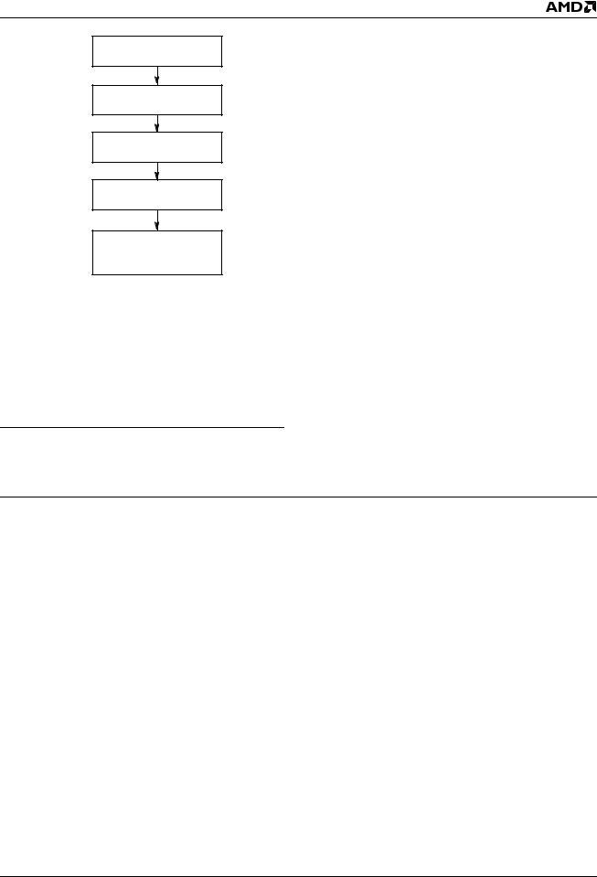
The primary method requires VID on the RESET# pin only, and can be implemented either in-system or via programming equipment. Figure 1 shows the algorithms and Figure 21 shows the timing diagram. This method uses standard microprocessor bus cycle timing. For sector unprotect, all unprotected sectors must first be protected prior to the first sector unprotect write cycle.
The alternate method intended only for programming equipment requires VID on address pin A9, OE#, and RESET#. This method is compatible with programmer routines written for earlier 3.0 volt-only AMD flash devices. Publication number 22134 contains further details; contact an AMD representative to request a copy.
The device is shipped with all sectors unprotected. AMD offers the option of programming and protecting sectors at its factory prior to shipping the device through AMD’s ExpressFlash™ Service. Contact an AMD representative for details.
It is possible to determine whether a sector is protected or unprotected. See “Autoselect Mode” for details.
Temporary Sector Unprotect
This feature allows temporary unprotection of previously protected sectors to change data in-system. The Sector Unprotect mode is activated by setting the RESET# pin to VID. During this mode, formerly protected sectors can be programmed or erased by selecting the sector addresses. Once VID is removed from the RESET# pin, all the previously protected sectors are protected again. Figure 2 shows the algorithm, and Figure 20 shows the timing diagrams, for this feature.
Am29LV001B |
10 |

|
|
|
P R E L I M I N A R Y |
|
|
|
|
START |
|
START |
|
|
|
|
|
|
|
|
|
PLSCNT = 1 |
Protect all sectors: |
PLSCNT = 1 |
|
|
|
The indicated portion |
|
||
|
|
|
of the sector protect |
|
|
|
|
RESET# = VID |
algorithm must be |
RESET# = VID |
|
|
|
|
performed for all |
|
|
|
|
Wait 1 μs |
unprotected sectors |
Wait 1 μs |
|
|
|
prior to issuing the |
|
||
|
|
|
|
|
|
|
|
|
first sector |
|
|
|
No |
|
unprotect address |
First Write |
No |
Temporary Sector |
First Write |
|
|||
|
|
Cycle = 60h? |
Temporary Sector |
||
Unprotect Mode |
|
Cycle = 60h? |
|
Unprotect Mode |
|
|
|
|
|||
|
|
Yes |
|
Yes |
|
|
|
Set up sector |
No |
All sectors |
|
|
|
address |
|
||
|
|
|
protected? |
|
|
|
|
|
|
|
|
|
|
Sector Protect: |
|
Yes |
|
|
|
Write 60h to sector |
|
|
|
|
|
|
|
|
|
|
|
address with |
|
Set up first sector |
|
|
|
A6 = 0, A1 = 1, |
|
|
|
|
|
|
address |
|
|
|
|
A0 = 0 |
|
|
|
|
|
|
|
|
|
|
|
Wait 150 µs |
|
Sector Unprotect: |
|
|
|
|
Write 60h to sector |
||
|
|
|
|
||
|
|
|
|
address with |
|
|
|
Verify Sector |
|
A6 = 1, A1 = 1, |
|
|
|
Protect: Write 40h |
|
A0 = 0 |
|
Increment |
|
to sector address |
Reset |
|
|
|
with A6 = 0, |
PLSCNT = 1 |
Wait 15 ms |
|
|
PLSCNT |
|
A1 = 1, A0 = 0 |
|
|
|
|
|
|
|
||
|
|
Read from |
|
Verify Sector |
|
|
|
|
Unprotect: Write |
|
|
|
|
sector address |
|
|
|
|
|
|
40h to sector |
|
|
|
|
with A6 = 0, |
|
|
|
|
|
|
address with |
|
|
|
|
A1 = 1, A0 = 0 |
Increment |
|
|
|
|
A6 = 1, A1 = 1, |
|
||
No |
|
|
|
||
|
|
PLSCNT |
|
||
|
|
A0 = 0 |
|
||
|
|
|
|
|
|
|
No |
|
|
|
|
PLSCNT |
|
Data = 01h? |
|
Read from |
|
= 25? |
|
|
|
sector address |
|
|
|
|
|
with A6 = 1, |
|
Yes |
|
Yes |
No |
A1 = 1, A0 = 0 |
|
|
|
|
Set up |
||
|
|
|
|
|
|
|
|
Yes |
No |
next sector |
|
|
|
address |
|||
Device failed |
|
Protect another |
PLSCNT |
Data = 00h? |
|
|
|
||||
|
sector? |
= 1000? |
|
|
|
|
|
|
|
||
|
|
No |
Yes |
Yes |
|
|
|
Remove VID |
|
|
No |
|
|
from RESET# |
Device failed |
Last sector |
|
|
|
|
verified? |
|
|
|
|
|
|
|
|
|
|
Write reset |
|
Yes |
|
|
|
command |
|
|
|
|
|
|
|
|
|
Sector Protect |
|
|
Sector Unprotect |
Remove VID |
|
|
Sector Protect |
from RESET# |
|
||
Algorithm |
|
complete |
Algorithm |
|
|
|
|
|
|
Write reset |
|
|
|
|
|
command |
|
|
|
|
|
Sector Unprotect |
|
|
|
|
|
complete |
|
21557C-4
Figure 1. In-System Sector Protect/Unprotect Algorithms
11 |
Am29LV001B |
P R E L I M I N A R Y
START
RESET# = VID
(Note 1)
against inadvertent writes (refer to Table 5 for command definitions). In addition, the following hardware data protection measures prevent accidental erasure or programming, which might otherwise be caused by spurious system level signals during VCC power-up and power-down transitions, or from system noise.
Low VCC Write Inhibit
Perform Erase or Program Operations
RESET# = VIH
Temporary Sector
Unprotect Completed
(Note 2)
When VCC is less than VLKO, the device does not accept any write cycles. This protects data during VCC
power-up and power-down. The command register and all internal program/erase circuits are disabled, and the device resets. Subsequent writes are ignored until VCC is greater than VLKO. The system must provide the proper signals to the control pins to prevent unintentional writes when VCC is greater than VLKO.
Write Pulse “Glitch” Protection
21557C-5
Notes:
1.All protected sectors unprotected.
2.All previously protected sectors are protected once again.
Figure 2. Temporary Sector Unprotect Operation
Hardware Data Protection
The command sequence requirement of unlock cycles for programming or erasing provides data protection
Noise pulses of less than 5 ns (typical) on OE#, CE# or WE# do not initiate a write cycle.
Logical Inhibit
Write cycles are inhibited by holding any one of OE# = VIL, CE# = VIH or WE# = VIH. To initiate a write cycle, CE# and WE# must be a logical zero while OE# is a logical one.
Power-Up Write Inhibit
If WE# = CE# = VIL and OE# = VIH during power up, the device does not accept commands on the rising edge of WE#. The internal state machine is automatically reset to reading array data on power-up.
COMMAND DEFINITIONS
Writing specific address and data commands or sequences into the command register initiates device operations. Table 5 defines the valid register command sequences. Writing incorrect address and data values or writing them in the improper sequence resets the device to reading array data.
All addresses are latched on the falling edge of WE# or CE#, whichever happens later. All data is latched on the rising edge of WE# or CE#, whichever happens first. Refer to the appropriate timing diagrams in the “AC Characteristics” section.
Reading Array Data
The device is automatically set to reading array data after device power-up. No commands are required to retrieve data. The device is also ready to read array data after completing an Embedded Program or Embedded Erase algorithm.
After the device accepts an Erase Suspend command, the device enters the Erase Suspend mode. The system can read array data using the standard read timings, except that if it reads at an address within erase-suspended sectors, the device outputs status data. After completing a programming operation in the Erase Suspend mode, the system may once again read array data with the same exception. See “Erase Suspend/Erase Resume Commands” for more information on this mode.
The system must issue the reset command to re-ena- ble the device for reading array data if DQ5 goes high, or while in the autoselect mode. See the “Reset Command” section, next.
See also “Requirements for Reading Array Data” in the “Device Bus Operations” section for more information. The Read Operations table provides the read parameters, and Figure 13 shows the timing diagram.
Am29LV001B |
12 |
 Loading...