


AMD Advanced Micro Devices AM27C020-55PI, AM27C020-55PC5, AM27C020-55PC, AM27C020-55JI5, AM27C020-55JI Datasheet
...
FINAL
Am27C020
2 Megabit (256 K x 8-Bit) CMOS EPROM
DISTINCTIVE CHARACTERISTICS
■ Fast access time |
■ Single +5 V power supply |
— Speed options as fast as 55 ns |
■ ±10% power supply tolerance standard |
■ Low power consumption |
■ 100% Flashrite™ programming |
— 100 µA maximum CMOS standby current |
— Typical programming time of 32 seconds |
■ JEDEC-approved pinout |
■ Latch-up protected to 100 mA from –1 V to |
— Plug in upgrade of 1 Mbit EPROM |
VCC + 1 V |
— Easy upgrade from 28-pin JEDEC EPROMs |
■ High noise immunity |
|
|
|
■ Compact 32-pin DIP, PDIP, and PLCC packages |
|
|
GENERAL DESCRIPTION |
|
The Am27C020 is a 2 Megabit, ultraviolet erasable programmable read-only memory. It is organized as 256 Kwords by 8 bits per word, operates from a single +5 V supply, has a static standby mode, and features fast single address location programming. Products are available in windowed ceramic DIP packages, as well as plastic one time programmable (OTP) PDIP and PLCC packages.
Data can be typically accessed in less than 55 ns, allowing high-performance microprocessors to operate without any WAIT states. The device offers separate Output Enable (OE#) and Chip Enable (CE#) controls,
thus eliminating bus contention in a multiple bus microprocessor system.
AMD’s CMOS process technology provides high speed, low power, and high noise immunity. Typical power consumption is only 100 mW in active mode, and 100 µW in standby mode.
All signals are TTL levels, including programming signals. Bit locations may be programmed singly, in blocks, or at random. The device supports AMD’s Flashrite programming algorithm (100 µs pulses), resulting in a typical programming time of 32 seconds.
BLOCK DIAGRAM

 VCC
VCC

 VSS
VSS

 VPP
VPP
OE# 
CE# 
PGM# 
A0–A17
Address 
Inputs
Output Enable
Chip Enable
and
Prog Logic
Y
Decoder
X
Decoder
Data Outputs
DQ0–DQ7
Output
Buffers
Y
Gating
2,097,152 Bit Cell Matrix
11507H-1
Publication# 11507 Rev: H Amendment/0
Issue Date: May 1998
PRODUCT SELECTOR GUIDE
Family Part Number |
|
|
|
Am27C020 |
|
|
|
|
|
|
|
|
|
|
|
|
|
Speed Options |
VCC = 5.0 V ± 5% |
-55 |
-75 |
|
|
|
|
-255 |
|
|
|
|
|
|
|
|
|
VCC = 5.0 V ± 10% |
55 |
-70 |
-90 |
-120 |
-150 |
-200 |
|
|
|
|
|||||||
|
|
|
|
|
|
|
|
|
Max Access Time (ns) |
55 |
70 |
90 |
120 |
150 |
200 |
250 |
|
|
|
|
|
|
|
|
|
|
CE# (E#) Access (ns) |
55 |
70 |
90 |
120 |
150 |
200 |
250 |
|
|
|
|
|
|
|
|
|
|
OE# (G#) Access (ns) |
35 |
40 |
40 |
50 |
65 |
75 |
100 |
|
|
|
|
|
|
|
|
|
|
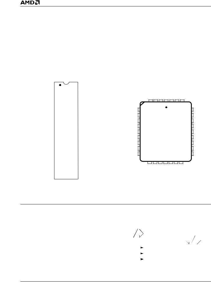
CONNECTION DIAGRAMS
Top View
DIP
VPP |
|
1 |
32 |
VCC |
|
|
|
||
A16 |
|
2 |
31 |
PGM# (P#) |
|
|
|
|
|
A15 |
|
3 |
30 |
A17 |
|
|
|
|
|
A12 |
|
4 |
29 |
A14 |
|
|
|
|
|
A7 |
|
5 |
28 |
A13 |
|
|
|
|
|
A6 |
|
6 |
27 |
A8 |
|
|
|
|
|
A5 |
|
7 |
26 |
A9 |
|
|
|
|
|
A4 |
|
8 |
25 |
A11 |
|
|
|
|
|
A3 |
|
9 |
24 |
OE# (G#) |
|
|
|
|
|
A2 |
|
10 |
23 |
A10 |
|
|
|
|
|
A1 |
|
11 |
22 |
CE# (E#) |
|
|
|
|
|
A0 |
|
12 |
21 |
DQ7 |
DQ0 |
|
|
|
DQ6 |
|
13 |
20 |
||
|
|
|
|
|
DQ1 |
|
14 |
19 |
DQ5 |
|
|
|
|
|
DQ2 |
|
15 |
18 |
DQ4 |
VSS |
|
|
|
|
|
16 |
17 |
DQ3 |
11507H-2
Notes:
PLCC
|
|
|
|
A12 |
A15 |
A16 |
|
|
|
|
(P#) |
A17 |
|
||||
|
|
|
|
V |
V |
PGM# |
|
||||||||||
|
|
|
|
|
|
|
|
|
|
PP |
CC |
|
|
|
|
||
|
|
|
|
|
3 |
2 |
1 |
32 31 30 |
|
||||||||
|
|
|
4 |
|
|||||||||||||
A7 |
5 |
|
|
|
|
|
|
|
|
|
|
|
|
|
29 |
A14 |
|
A6 |
6 |
|
|
|
|
|
|
|
|
|
|
|
|
|
28 |
A13 |
|
A5 |
7 |
|
|
|
|
|
|
|
|
|
|
|
|
|
27 |
A8 |
|
A4 |
8 |
|
|
|
|
|
|
|
|
|
|
|
|
|
26 |
A9 |
|
A3 |
9 |
|
|
|
|
|
|
|
|
|
|
|
|
|
25 |
A11 |
|
A2 |
10 |
|
|
|
|
|
|
|
|
|
|
|
|
24 |
OE# (G#) |
||
A1 |
11 |
|
|
|
|
|
|
|
|
|
|
|
|
23 |
A10 |
||
A0 |
12 |
|
|
|
|
|
|
|
|
|
|
|
|
22 |
CE# (E#) |
||
DQ0 |
13 |
|
|
|
|
|
|
|
|
|
|
|
|
21 |
DQ7 |
||
|
14 15 16 17 18 19 20 |
|
|||||||||||||||
|
|
|
|
|
|
|
|
|
|
|
|
|
|
|
|
|
|
|
|
|
|
DQ1 |
DQ2 |
SS |
DQ3 |
DQ4 |
DQ5 |
DQ6 |
|
||||||
|
|
|
|
V |
|
||||||||||||
11507H-3
1.JEDEC nomenclature is in parenthesis.
2.The 32-pin DIP to 32-pin PLCC configuration varies from the JEDEC 28-pin DIP to 32-pin PLCC configuration.
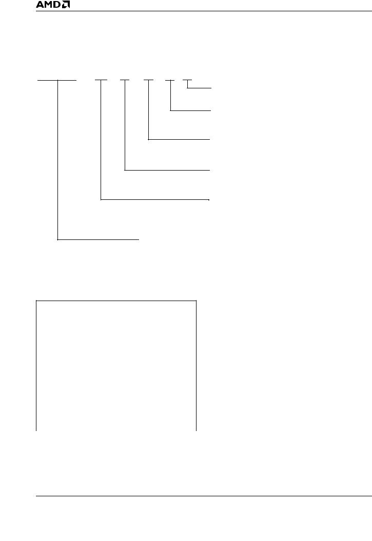
PIN DESIGNATIONS |
LOGIC SYMBOL |
|
|
|
||||||
A0–A17 |
= |
Address Inputs |
|
|
|
|
|
|
|
|
|
|
|
|
|
|
|
|
|||
CE# (E#) |
= |
Chip Enable Input |
18 |
|
|
|
|
|
|
|
|
|
|
|
|
|
|
|
|
||
DQ0–DQ7 |
= |
Data Input/Outputs |
|
|
|
|
A0–A17 |
|
8 |
|
|
|
|
|
|
||||||
|
|
|
|
|
||||||
|
|
|
|
|
|
|
|
|||
OE# (G#) |
= |
Output Enable Input |
|
|
|
|
|
DQ0–DQ7 |
|
|
|
|
|
|
|
|
|
||||
|
|
|
|
|
|
|
||||
PGM# (P#) |
= |
Program Enable Input |
|
|
|
|
|
|
|
|
|
|
|
|
CE# (E#) |
|
|
|
|||
|
|
|
|
|
|
|
||||
VCC |
= |
VCC Supply Voltage |
|
|
|
|
|
|
|
|
|
|
|
|
|
|
|
||||
|
|
|
|
PGM# (P#) |
|
|
|
|||
VPP |
= |
Program Voltage Input |
|
|
|
|
|
|
|
|
|
|
|
|
OE# (G#) |
|
|
|
|||
|
|
|
|
|
|
|
||||
VSS |
= Ground |
|
|
|
|
|
|
|
|
|
11507H-4
2 |
Am27C020 |

ORDERING INFORMATION
UV EPROM Products
AMD standard products are available in several packages and operating ranges. The order number (Valid Combination) is formed by a combination of the following:
AM27C020 |
-55 |
|
D |
|
C |
5 |
|
B |
|
|||||||||
|
|
|
|
|
|
|
|
|
|
|
|
|
|
|
|
|
OPTIONAL PROCESSING |
|
|
|
|
|
|
|
|
|
|
|
|
|
|
|
|
|
|
||
|
|
|
|
|
|
|
|
|
|
|
|
|
|
|
|
|
Blank = Standard Processing |
|
|
|
|
|
|
|
|
|
|
|
|
|
|
|
|
|
|
B |
= Burn-In |
|
|
|
|
|
|
|
|
|
|
|
|
|
|
|
|
|
VOLTAGE TOLERANCE |
|
|
|
|
|
|
|
|
|
|
|
|
|
|
|
|
|
|
||
|
|
|
|
|
|
|
|
|
|
|
|
5 |
= VCC ± 5%, 55 ns only |
|||||
|
|
|
|
|
|
|
|
|
|
|
|
|
|
|
|
|
See Product Selector Guide and Valid Combinations |
|
|
|
|
|
|
|
|
|
|
|
|
|
|
|
|
|
|
TEMPERATURE RANGE |
|
|
|
|
|
|
|
|
|
|
|
|
|
|
|
|
|
|
||
|
|
|
|
|
|
|
|
|
|
|
|
|
|
|
|
|
C |
= Commercial (0°C to +70°C) |
|
|
|
|
|
|
|
|
|
|
|
|
|
|
|
|
|
I |
= Industrial (–40°C to +85°C) |
|
|
|
|
|
|
|
|
|
|
|
|
|
|
|
|
|
E |
= Extended (–55°C to +125°C) |
|
|
|
|
|
|
|
|
|
|
|
|
|
|
|
|
|
PACKAGE TYPE |
|
|
|
|
|
|
|
|
|
|
|
|
|
|
|
|
|
|
||
|
|
|
|
|
|
|
|
|
|
|
|
|
|
|
|
|
D |
= 32-Pin Ceramic DIP (CDV032) |
SPEED OPTION
See Product Selector Guide and Valid Combinations
DEVICE NUMBER/DESCRIPTION
Am27C020
2 Megabit (256 K x 8-Bit) CMOS UV EPROM
Valid Combinations
AM27C020-55 |
DC5, DC5B, DI5, DI5B |
|
VCC = 5.0 V ± 5% |
||
|
||
AM27C020-55 |
|
|
VCC = 5.0 V ± 10% |
|
|
|
DC, DCB, DI, DIB |
|
AM27C020-70 |
||
|
||
|
|
|
AM27C020-90 |
|
|
|
|
|
AM27C020-120 |
|
|
|
|
|
AM27C020-150 |
DC, DCB, DI, DIB, DE, DEB |
|
|
|
|
AM27C020-200 |
|
|
|
|
|
AM27C020-255 |
DC, DCB, DI, DIB |
|
VCC = 5.0 V ± 5% |
||
|
Valid Combinations
Valid Combinations list configurations planned to be supported in volume for this device. Consult the local AMD sales office to confirm availability of specific valid combinations and to check on newly released combinations.
Am27C020 |
3 |
ORDERING INFORMATION
OTP EPROM Products
AMD standard products are available in several packages and operating ranges. The order number (Valid Combination) is formed by a combination of the following:
AM27C020 |
-55 |
J |
C |
5 |
OPTIONAL PROCESSING
Blank = Standard Processing
VOLTAGE TOLERANCE
5 = VCC ± 5%, 55 ns only
See Product Selector Guide and Valid Combinations
TEMPERATURE RANGE
C = Commercial (0°C to +70°C)
I = Industrial (–40°C to +85°C)
PACKAGE TYPE
P = 32-Pin Plastic DIP (PD 032)
J = 32-Pin Plastic Leaded Chip Carrier (PL 032)
SPEED OPTION
See Product Selector Guide and Valid Combinations
DEVICE NUMBER/DESCRIPTION
Am27C020
2 Megabit (256 K x 8-Bit) CMOS OTP EPROM
Valid Combinations
AM27C020-55 |
PC5, PI5, JC5, JI5 |
|
VCC = 5.0 V ± 5% |
||
|
||
AM27C020-55 |
|
|
VCC = 5.0 V ± 10% |
|
|
AM27C020-75 |
|
|
|
|
|
AM27C020-90 |
|
|
|
|
|
AM27C020-120 |
JC, PC, JI, PI |
|
|
|
|
AM27C020-150 |
|
|
|
|
|
AM27C020-200 |
|
|
|
|
|
AM27C020-255 |
|
|
VCC = 5.0 V ± 5% |
|
Valid Combinations
Valid Combinations list configurations planned to be supported in volume for this device. Consult the local AMD sales office to confirm availability of specific valid combinations and to check on newly released combinations.
4 |
Am27C020 |
 Loading...