


AM29LV008BB-70REIB
Table of contents
 Loading...
AMD Advanced Micro Devices AM29LV008BB-70REIB, AM29LV008BB-70REI, AM29LV008BB-70REEB, AM29LV008BB-70REE, AM29LV008BB-70REC Datasheet
...
PRELIMINARY
This document contains information on a product under development at Advanced Micro Devices. The information
is intended to help you ev aluate this product. AMD reserves the right to change or dis continue work on thi s proposed
product without notice.
Publication# 21524 Rev: B Amendment/+1
Issue Date: March 1998
Refer to AMD’s Website (www.amd.com) for the latest information.
Am29LV008B
8 Megabit (1 M x 8-Bit)
CMOS 3.0 Volt-onl y Boot Sector Flash Memory
DISTINCTIVE CHARACTERISTICS
■ Single power supply operation
— Full voltage range: 2.7 to 3. 6 volt read and write
operations for battery-powered applications
— Regulated voltage range: 3.0 to 3. 6 volt read
and write operations and for compatibility with
high performance 3.3 volt microprocessors
■ Manufactured on 0.35 µm process technology
— Compatible with 0.5 µm Am29LV008 device
■ High performance
— Full voltage range: ac cess times as f ast as 80 ns
— Regulated voltage range: access times as fast
as 70 ns
■ Ultra low power consumption (typical values at
5 MHz)
— 200 nA Automatic Sleep mode current
— 200 nA standby mode current
— 7 mA read current
— 15 mA program/erase current
■ Flexible sector architecture
— One 16 Kbyte, two 8 Kbyte, one 32 Kbyte, and
fifteen 64 Kbyte sectors
— Supports full chip erase
— Sector Protection features:
A hardware method of locking a sector to
prevent any program or erase operations within
that sector
Sectors can be locked in-system or via
programming equipment
T emporary Sector Unprotect feat ure allows code
changes in previously locked sectors
■ Unlock Bypass Program Command
— Reduces overall programming time when
issuing multiple program command sequences
■ Top or bottom boot block configurations
available
■ Embedded Al gorithms
— Embedded Erase algorithm automatically
preprograms and erases the entire chip or any
combination of designated sectors
— Embedded Program algorithm automatically
writes and verifies data at specified addresses
■ Minimum 1,000,000 write cycle guarantee per
sector
■ Package option
— 40-pin TSOP
■ Compatibility with JEDEC standards
— Pinout and software compatible with single-
power supply Flash
— Superior inadvertent write protection
■ Data# Polling and toggle bits
— Provides a software method of detecting
program or erase operation completion
■ Ready/Busy# pin (RY/BY#)
— Provides a hardware method of detecting
program or erase cycle completion
■ Erase Suspend/Erase Resume
— Suspends an erase operati on to read dat a from,
or program data to, a sector that is not being
erased, then resumes the erase operation
■ Hardware reset pin (RESET#)
— Hardware method to reset the de vi ce to reading
array data

2 Am29LV008B
PRELIMINARY
GENERAL DESCRIPTION
The Am29LV008B is an 8 Mbit, 3.0 volt-only Flash
memory organized as 1,048,576 bytes. The device is
offered in a 40-pin TSOP package. The byte-wide (x8)
data appears on DQ7–DQ0. This device requires only
a single, 3.0 volt V
CC
supply to perform read, program,
and erase operations. A stand ard EPROM pro-
grammer can also be used to program and erase the
device.
This device is manufactured using AMD’s 0.35 µm
process technology, and offers all the features and
benefits of the Am29LV008, which was manufactured
using 0.5 µm process technology. In addition, the
Am29LV008B features unlock bypass programming
and in-system sector protection/unprotection.
The standard device offers access times of 70, 80, 90,
and 120 ns, allowing high speed microprocessors to
operate without wait s tates. To eliminate bus conten-
tion the device has separate chip enable (CE#), write
enable (WE#) and output enable (OE#) controls.
The device requires only a single 3. 0 v o lt po wer sup-
ply for both read and write functions. Internally gener-
ated and regulated voltages are provided for the
program and erase operations.
The device is entirely command set compatible with the
JEDEC single-power-supply Flash standard. Com-
mands are written to the command regis ter using
standard micropr ocessor wri te timings. Register co n-
tents serve as input to an internal state-machine that
controls the erase and programming circuitry. Write
cycles also internally latch addresses and data needed
for the programming and erase operations. Reading
data out of the device is similar to reading from other
Flash or EPROM devices.
Device programming occurs by executing the program
command sequence. This initiates the Embedded
Program algorithm—an internal algorithm that auto-
matically times the program pulse widths and verifies
proper cell margin. The Unlock Bypass mode facili-
tates faster programming times by requir ing only two
write cycles to program data instead of four.
Device erasure occurs by ex ecuting the erase command
sequence. This initiates the Embedded Erase algo-
rithm—an i nternal algorithm that autom atically prepro -
grams the array (if it is not already programmed) before
executing the erase operation. During erase, the device
automatically times the erase pulse widths and verifies
proper cell margin.
The host system can detect whether a program or
erase operation is complete by observing the RY/BY#
pin, or by reading the DQ7 (Data# Polling) and DQ6
(toggle) status bits. After a program or erase cycle
has been completed, the device is ready to read array
data or accept another command.
The sector erase ar chitecture allo ws memo ry secto rs
to be erased and reprogrammed without affecting the
data contents of other sectors. The device is fully
erased when shipped from the factory.
Hardware data protection measures include a low
V
CC
detector that automatically in hibits write opera-
tions during power transitions. The hardware sector
protection feature disables both program and erase
operations in any combination of the sectors of mem-
ory. This can be achieved in-system or via program-
ming equipment.
The Erase Suspend feature enables the user to put
erase on hold for any period of time to read data from,
or program data to, any sector that is not selected for
erasure. True background erase can thus be achieved.
The hardware RESET# pi n terminates any operation
in progress and resets the internal state machine to
reading array dat a. The RESET# pin ma y be tied to the
system reset circuitry. A system reset would thus also
reset the device, enabling the system microprocessor
to read the boot-up firmware from the Flash memory.
The device offers two power-saving features. When
addresses have been stable for a specified amount of
time, the device enters the automatic sleep m ode.
The system can also place the de vice into the standby
mode. Power consumption is greatly reduced in both
these modes.
AMD’s Flash technology combines years of Flash
memory manufacturing experience to produce the
highest levels of quality, reliability and cost effective-
ness. The device electrically erases a ll bit s within
a sector simultaneously via Fowler-Nordheim tun-
neling. The data is programmed using hot electron
injection.
Am29LV008B 3
PRELIMINARY
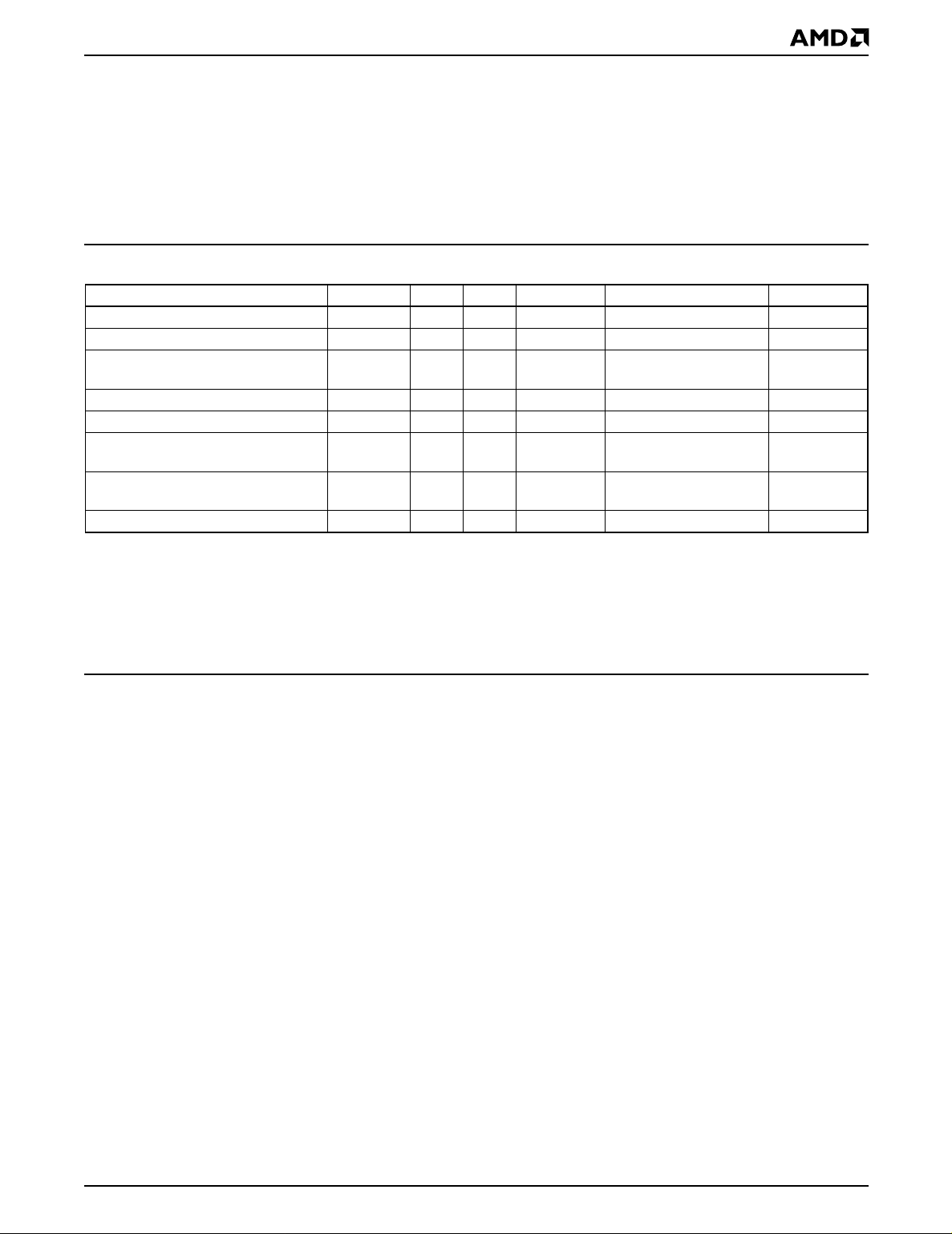
PRODUCT SELECTOR GUIDE
Note: See “AC Characte r ist ics ” for full specifications.
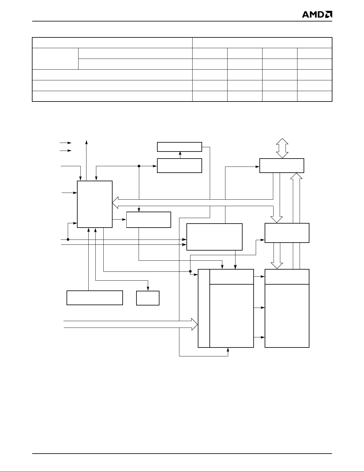
BLOCK DIAGRAM
Family Part Number Am29LV008B
Speed Options
Regulated Voltage Range: V
CC
=3.0–3.6 V -70R
Full Voltage Range: V
CC
= 2.7–3.6 V -80 -90 -120
Max access time, ns (t
ACC
) 70 80 90 120
Max CE# access time, ns (t
CE
) 70 80 90 120
Max OE# access time, ns (t
OE
) 30 30 35 50
Input/Output
Buffers
X-Decoder
Y-Decoder
Chip Enable
Output Enable
Logic
Erase Voltage
Generator
PGM Voltage
Generator
Timer
V
CC
Detector
State
Control
Command
Register
V
CC
V
SS
WE#
CE#
OE#
STB
STB
DQ0
–
DQ7
Sector Switches
RY/BY#
RESET#
Data
Latch
Y-Gating
Cell Matrix
Address Latch
A0–A19
21524B-1
4 Am29LV008B
PRELIMINARY
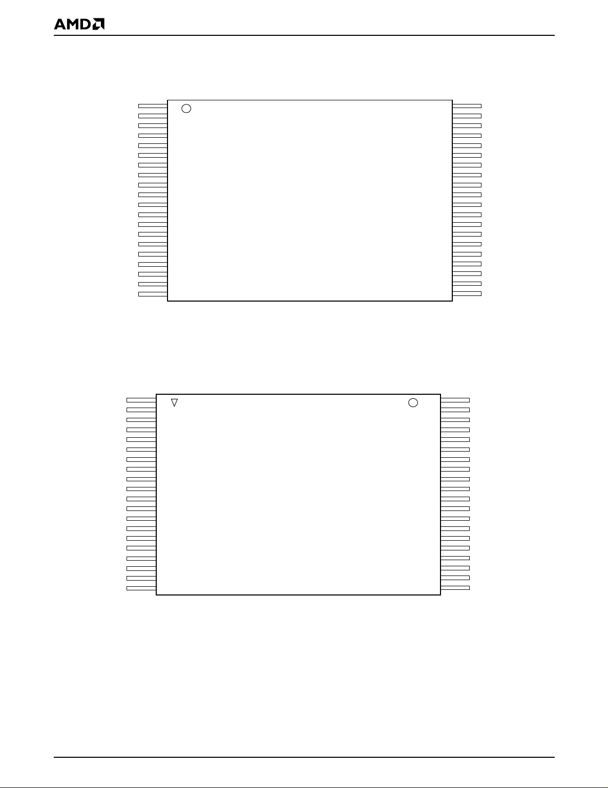
CONNECTION DIAGRAMS
1
16
2
3
4
5
6
7
8
17
18
19
20
9
10
11
12
13
14
15
40
25
39
38
37
36
35
34
33
32
31
30
29
28
27
26
24
23
22
21
A16
A5
A15
A14
A13
A12
A11
A9
A8
WE#
RESET#
NC
RY/BY#
A18
A7
A6
A4
A3
A2
A1
A17
DQ0
V
SS
NC
A19
A10
DQ7
DQ6
DQ5
OE#
V
SS
CE#
A0
DQ4
V
CC
V
CC
NC
DQ3
DQ2
DQ1
1
16
2
3
4
5
6
7
8
17
18
19
20
9
10
11
12
13
14
15
40
25
39
38
37
36
35
34
33
32
31
30
29
28
27
26
24
23
22
21
A16
A5
A15
A14
A13
A12
A11
A9
A8
WE#
RESET#
NC
RY/BY#
A18
A7
A6
A4
A3
A2
A1
A17
DQ0
V
SS
NC
A19
A10
DQ7
DQ6
DQ5
CE#
V
SS
CE#
A0
DQ4
V
CC
V
CC
NC
DQ3
DQ2
DQ1
21524B-2
Reverse TSOP
Standard TSOP
Am29LV008B 5
PRELIMINARY
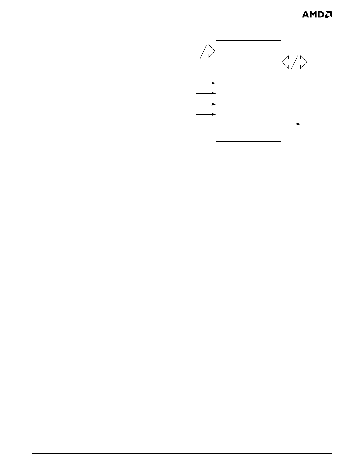
PIN CONFIGURATION
A0–A19 = 20 addresses
DQ0–DQ7 = 8 data inputs/outputs
CE# = Chip enable
OE# = Output enable
WE# = Write enable
RESET# = Hardware reset pin, active low
RY/BY# = Ready/Busy# output
V
CC
= 3.0 volt-only single power supply
(see Product Selector Guide for speed
options and voltage supply toleranc es)
V
SS
= Device ground
NC = Pin not connected internally
LOGIC SYMBOL
21524B-3
20
8
DQ0–DQ7
A0–A19
CE#
OE#
WE#
RESET#
RY/BY#
6 Am29LV008B
PRELIMINARY
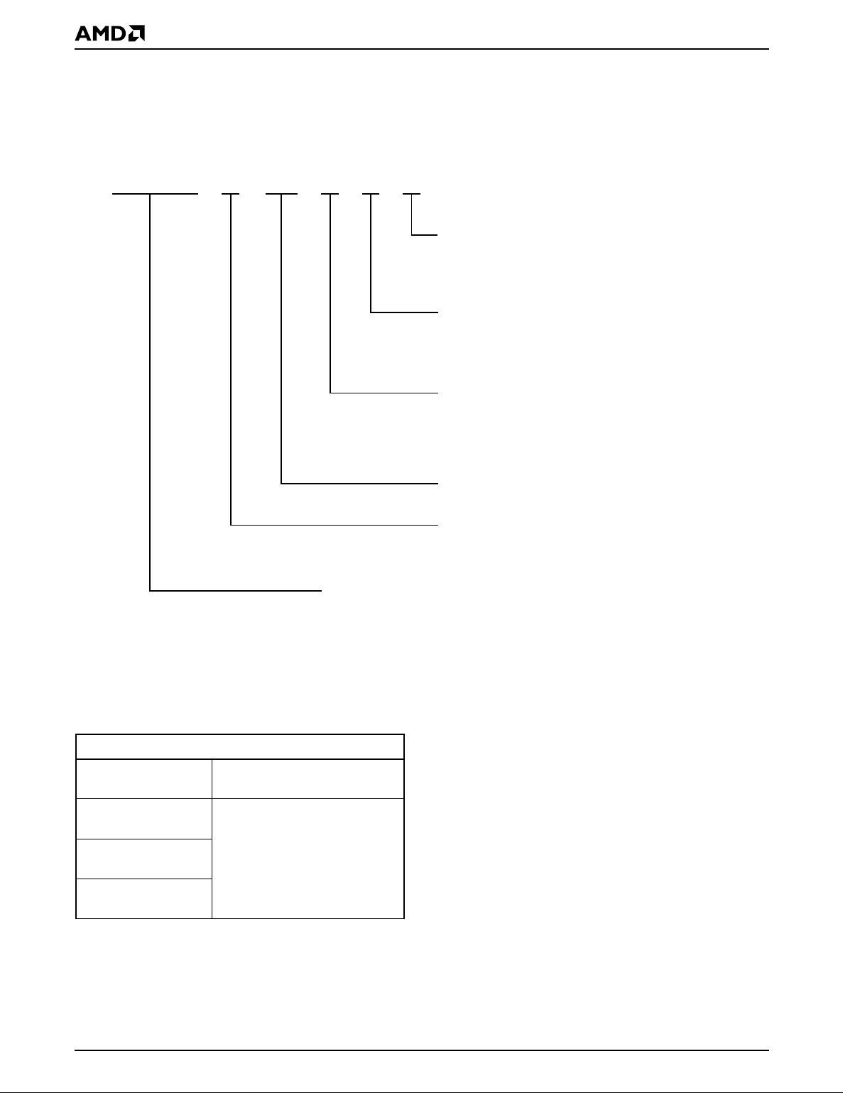
ORDERING INFORMATION
Standard Pr od ucts
AMD standard products are available in s everal packages and operating ranges. The order number (Valid Combi-
nation) is formed by a combination of the elements below.
Valid Combinations
Valid Combinations list configurations planned to be sup-
ported in volume for this device. Consult the local AMD sales
office to confirm availability of specific valid combinations and
to check on newly released combinations.
DEVICE NUMBER/DESCRIPTION
Am29LV008B
8 Megabit (1 M x 8-Bit) CMOS Flash Memory
3.0 Volt-only Read, Program, and Erase
CE-70RAm29LV008B T
OPTIONAL PROCESSING
Blank = Standard Processing
B = Burn-in
(Contact an AMD representative for more information)
TEMPERATURE RANGE
C=Commercial (0°C to +70°C)
I = Industrial (–40°C to +85°C)
E = Extended (–55°C to +125°C)
PACKAGE TYPE
E = 40-Pin Thin Small Outline Package (TSOP)
Standard Pinout (TS 040)
F = 40-Pin Thin Small Outline Package (TSOP)
Reverse Pinout (TSR040)
SPEED OPTION
See Product Selector Guide and Valid Combinations
BOOT CODE SECTOR ARCHITECTURE
T = Top Sector
B = Bottom Sector
Valid Combinations
Am29LV008BT-70R,
Am29LV008BB-70R
EC, EI, FC, FI
Am29LV008BT-80,
Am29LV008BB-80
EC, EI, EE, FC, FI, FE
Am29LV008BT-90,
Am29LV008BB-90
Am29LV008BT-120,
Am29LV008BB-120
Am29LV008B 7
PRELIMINARY
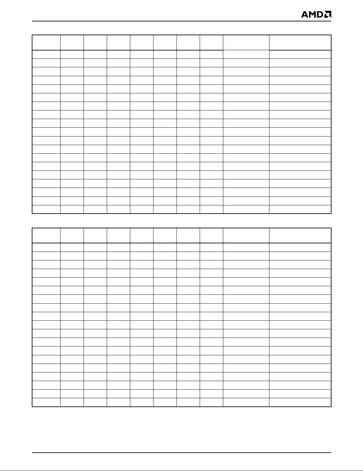
DEVICE BUS OPERATIONS
This section describes the requirements and use of the
device bus operations, which are initiated through the
internal command register. The command register itself
does not occupy any addressable memory loc ation.
The register is composed of latches that store the com-
mands, along with the address and data information
needed to execute the command. The contents of the
register serve as inputs to the internal state machine.
The state machine outputs d ictate the function of the
device. Table 1 lists the device bus operations, the
inputs and control lev els t he y requ ire , and t he resulting
output. The following subsections describe each of
these operations in further detail.
Table 1. Am29LV008B Device Bus Operations
Legend:
L = Logic Low = V
IL
, H = Logic High = V
IH
, V
ID
= 12.0
±
0.5 V, X = Don’t Care, A
IN
= Address In, D
IN
= Data In, D
OUT
= Data Out
Notes:
1. Addresses are A19–A0.
2. The sector protect and sector unprotect functions may also be implemented via programming equipment. See the “Sector
Protection/Unprotection” section.
Requirements for Reading Array Data
To read array data from the outputs, the system must
drive the CE# and OE# pins to V
IL
. CE# is the power
control and selects the device. OE# is the output
control and gates array data to the output pins. WE#
should remain at V
IH
.
The internal state machine is set for reading arr ay data
upon device power-up, or after a hardware reset. This
ensures that no spurious alteration of the mem ory
content occurs during the power transition. No
command is neces sary in this mode to obtain ar ray
data. Standard microprocessor read cycles that assert
valid addresses on the device address inputs produce
valid data on the device data outputs. The device
remains enabled for read access until the command
register contents are altered.
See “Reading Array Data” for more information. Refer
to the AC Read Operations table fo r timing specifica-
tions and to Figure 13 for the timing waveforms. I
CC1
in
the DC Characteristics table represents the active
current specification for reading array data.
Writing Commands/Command Sequences
To write a command or command sequence (which
includes programming data to the device and erasing
sectors of memory), the system must drive WE# and
CE# to V
IL
, and OE# to V
IH
.
The Am29LV008B is manufactured on AMD’s new 0.35
µm process technol ogy and offers an Unlock Bypass
mode to facilitate faster programming. Once the device
enters the Unlock Bypass mode, only two write cycles
are required to program a byte, instead of four. Devices
manufactured on AMD’s 0.5 µm process technology re-
quire a four-bus-cycle command sequence for each byte
programmed. The “Byte Program Command Sequence”
section has details on programm ing data to the device
using both standard and U nlock Bypass command se-
quences.
An erase operation can erase one sect or, multiple sec-
tors, or the entire device. Tables 2 and 3 indicate the
address space that each sector occupies. A “sector
address” consists of the address bits required to
uniquely select a sector. The “Command Definitions”
Operation CE# OE# WE# RESET# Addresses (Note 1) DQ0–DQ7
Read L L H H A
IN
D
OUT
Write L H L H A
IN
D
IN
Standby
V
CC
±
0.3 V
XX
V
CC
±
0.3 V
X High-Z
Output Disable L H H H X High-Z
Reset X X X L X High-Z
Sector Protect (Note 2) L H L V
ID
Sector Address, A6 = L,
A1 = H, A0 = L
D
IN
, D
OUT
Sector Unprotect (Note 2) L H L V
ID
Sector Address, A6 = H,
A1 = H, A0 = L
D
IN
, D
OUT
Temporary Sector Unprotect X X X V
ID
A
IN
D
IN

8 Am29LV008B
PRELIMINARY
section has details on erasing a sector or the entire
chip, or suspending/resuming the erase operation.
After the system writes the autoselect command
sequence, the devi ce enters the autoselect mode. The
system can then read autoselect codes from the
internal register (which is separate from the memory
array) on DQ7–DQ0. Standard read cycle timings
apply in this mode. Refer to the Autoselect Mode and
Autoselect Command Sequence sections for more
information.
I
CC2
in the DC Characteristics table represents the
active current specification for the write mode. The “A C
Characteristics” section contains timing specification
tables and timing diagrams for w r ite operations.
Program and Erase Operation Status
During an erase or program operation, the system ma y
check the status of the operation by reading the status
bits on DQ7–DQ0. Standard read cycle timings and I
CC
read specifications apply. Refer to “Write Operation
Status” for more information, and to “AC Characteris-
tics” for timing diagrams.
Standby Mode
When the system is not reading or writing to the device ,
it can place the device in the standby mode. In this
mode, current consumption is great ly reduc ed, and the
outputs are placed in the high impedance state, inde-
pendent of the OE# input.
The device enters the CMOS standby mode when the
CE# and RESET# pin s are both held at V
CC
± 0.3 V.
(Note that this is a more restricted voltage range than
V
IH
.) If CE# and RESET# ar e held a t V
IH
, but not within
V
CC
± 0.3 V, the device will be in the standb y mode, b ut
the standby current will be greater. The device requires
standard access time (t
CE
) for read access when the
device is in either of these standby modes, before it is
ready to read data.
If the device is deselected during erasure or program-
ming, the device draws active current until the
operation is completed.
In the DC Characteristics table, I
CC3
and I
CC4
repre-
sents the standby current s pecification.
Automatic Sleep Mode
The automatic sleep mode minimizes Flash device
energy consumption. The device automatically
enables this mode when addres ses remain stable for
t
ACC
+ 30 ns. The automatic sleep mode is inde-
pendent of the CE#, WE#, and OE# control signals.
Standard address access timings provide new data
when addresses are changed. While in sleep mode,
output data is latched and always available to the
system. I
CC5
in the DC Characteristics table represents
the automatic sleep mode current specification.
RESET#: Hardware Reset Pin
The RESET# pin provides a hardw are method of reset-
ting the device to reading array data. When the
RESET# pin is driven low for at least a period of t
RP
, the
device immediately terminates any operation in
progress, tristates all output pins, and ignores all
read/write commands for the duration of the RESET#
pulse. The device also resets the internal state
machine to reading array data. The operation that was
interrupted should be reinitiated once the device is
ready to accept another command sequence, to
ensure data integrity.
Current is reduced for the duration of the RESET#
pulse. When RESET# is held at V
SS
±0.3 V, the device
draws CMOS standby c urrent (I
CC4
). If RESET# is held
at V
IL
but not within V
SS
±0.3 V, the standby current will
be greater.
The RESET# pin may be tied to the system reset cir-
cuitry. A system reset would thus also reset the Flash
memory, enabling the system to read the boot-up
firmware from the Flash memory.
If RESET# is asserted during a program or erase oper-
ation, the RY/BY# pin remains a “0” (busy) until the
internal reset operation is complete, which requires a
time of t
READY
(during Embedded Algorithms). The
system can thus monitor RY/BY# to determine whether
the reset operation is complete. If RESET# is asserted
when a program or erase operation is not executing
(RY/BY# pin is “1”), the reset operation is completed
within a time of t
READY
(not during Embe dded Algo-
rithms). The system can read data t
RH
after the
RESET# pin returns to V
IH
.
Refer to the AC Characteristics tables for RESET# pa-
rameters and to Figure 14 for the timing diagram.
Output Disable Mode
When the OE# input is at V
IH
, output from the device is
disabled. The output pins are placed in t he high imped-
ance state.
Am29LV008B 9
PRELIMINARY
Table 2. Am29LV008BT Top Boot Block Sector Address Table
Table 3. Am29LV008BB Bottom Boot Block Sector Address Table
Sector A19 A18 A17 A16 A15 A14 A13
Sector Size
(Kbytes)
Address Range
(in hexadecimal)
SA00000XXX 64 00000h–0FFFFh
SA10001XXX 64 10000h–1FFFFh
SA20010XXX 64 20000h–2FFFFh
SA30011XXX 64 30000h–3FFFFh
SA40100XXX 64 40000h–4FFFFh
SA50101XXX 64 50000h–5FFFFh
SA60110XXX 64 60000h–6FFFFh
SA70111XXX 64 70000h–7FFFFh
SA81000XXX 64 80000h–8FFFFh
SA91001XXX 64 90000h–9FFFFh
SA101010XXX 64 A0000h–AFFFFh
SA111011XXX 64 B0000h–BFFFFh
SA121100XXX 64 C0000h–CFFFFh
SA131101XXX 64 D0000h–DFFFFh
SA141110XXX 64 E0000h–EFFFFh
SA1511110XX 32 F0000h–F7FFFh
SA161111100 8 F8000h–F9FFFh
SA171111101 8 FA000h–FBFFFh
SA18111111X 16 FC000h–FFFFFh
Sector A19 A18 A17 A16 A15 A14 A13
Sector Size
(Kbytes)
Address Range
(in hexadecimal)
SA0000000X 16 00000h-03FFFh
SA10000010 8 04000h-05FFFh
SA20000011 8 06000h-07FFFh
SA300001XX 32 08000h-0FFFFh
SA40001XXX 64 10000h-1FFFFh
SA50010XXX 64 20000h-2FFFFh
SA60011XXX 64 30000h-3FFFFh
SA70100XXX 64 40000h-4FFFFh
SA80101XXX 64 50000h-5FFFFh
SA90110XXX 64 60000h-6FFFFh
SA100111XXX 64 70000h-7FFFFh
SA111000XXX 64 80000h-8FFFFh
SA121001XXX 64 90000h-9FFFFh
SA131010XXX 64 A0000h-AFFFFh
SA141011XXX 64 B0000h-BFFFFh
SA151100XXX 64 C0000h-CFFFFh
SA161101XXX 64 D0000h-DFFFFh
SA171110XXX 64 E0000h-EFFFFh
SA181111XXX 64 F0000h-FFFFFh
10 Am29LV008B
PRELIMINARY
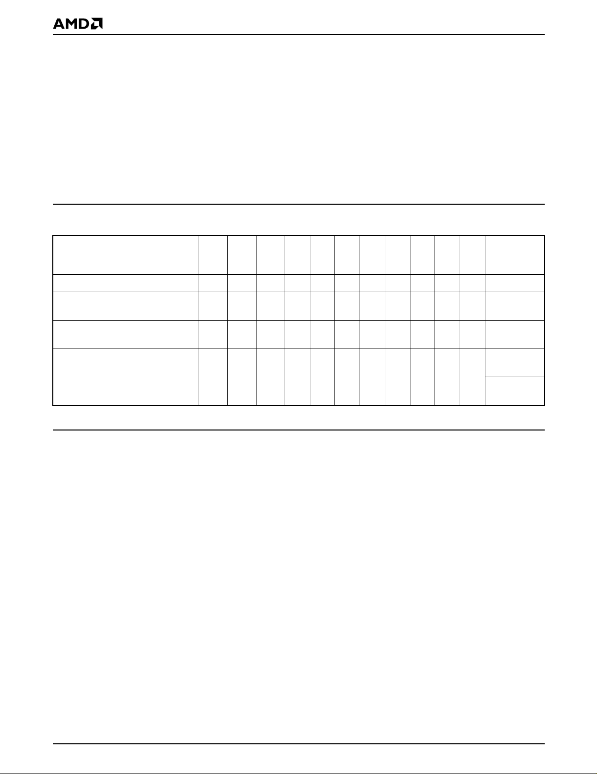
Autoselect Mode
The autoselect mode provides manufacturer and
device identification, and sector protection ver ification,
through identifier codes output on DQ7–DQ0. This
mode is primarily intended for progr amming equipment
to automatically match a device to be progr ammed with
its correspondi ng programming al gorithm. However,
the autoselect codes can also be accessed in-system
through the command register.
When using programming equipment, the autoselect
mode requires V
ID
(11.5 V to 12.5 V) on address pin
A9. Address pins A6, A1, and A0 must be as shown in
Table 4. In addition, when verifying sector protec tion,
the sector address must appear on the appropriate
highest order address bits (see Tables 2 and 3). Table
4 shows the remaining address bits that are don’t care .
When all necessary bits have been set as required, the
programming equipment may then read the corre-
sponding identifier code on DQ7–DQ0.
To access the autoselect codes in-system, the host
system can issue the autoselect command via the
command register, as shown in Table 5. This method
does not require V
ID
. See “Command Definitions” for
details on using the autoselect mode.
Table 4. Am29LV008B Autoselect Codes (High Voltage Method)
L = Logic Low = V
IL
, H = Logic High = V
IH
, SA = Sector Address, X = Don’t care.
Sector Protection/Unprotection
The hardware sector protection feature disables both
program and erase operations in any sect or. The hard-
ware sector unprotection feature re-enables both
program and erase operations in previously protected
sectors.
The device is shipped with all s ectors unprotected.
AMD offers the option of programming and protecting
sectors at its factory prior to shipping the device
through AMD’s ExpressFlash™ Servic e. Contact an
AMD representative for details.
It is possible to determine whether a sector is protected
or unprotected. See “Autoselect Mode” for details.
Sector protection/unprotection can be implemented via
two methods.
The primary method requires V
ID
on the RESET# pin
only, and c an be implemented either in-system or via
programming equipment. Figure 2 shows the algo-
rithms and Figure 21 shows the waveform. This
method uses standard microprocessor bus cycle
timing. For sector unprotect, all unprotected sectors
must first be protected prior to th e first s ector unprotec t
write cycle.
The alternate method intended o nly for programming
equipment requires V
ID
on address pin A9 and OE#.
This method is compatible with programmer routines
written for earlie r 3.0 volt-only AMD flash devices.
Details on this method are provided in a supplement,
publication number 20875. Contact an AMD represent-
ative to request a cop y.
Description CE# OE# WE#
A19
to
A13
A12
to
A10 A9
A8
to
A7 A6
A5
to
A2 A1 A0
DQ7
to
DQ0
Manufacturer ID: AMD L L H X X V
ID
XLXLL 01h
Device ID: Am29LV0 08B T
(Top Boot Block)
LLHXXV
ID
XLXLH 3Eh
Device ID: Am29LV0 08B B
(Bottom Boot Block)
LLHXXV
ID
XLXLH 37h
Sector Protection Verification L L H SA X V
ID
XLXHL
01h
(protected)
00h
(unprotected)
Am29LV008B 11
PRELIMINARY
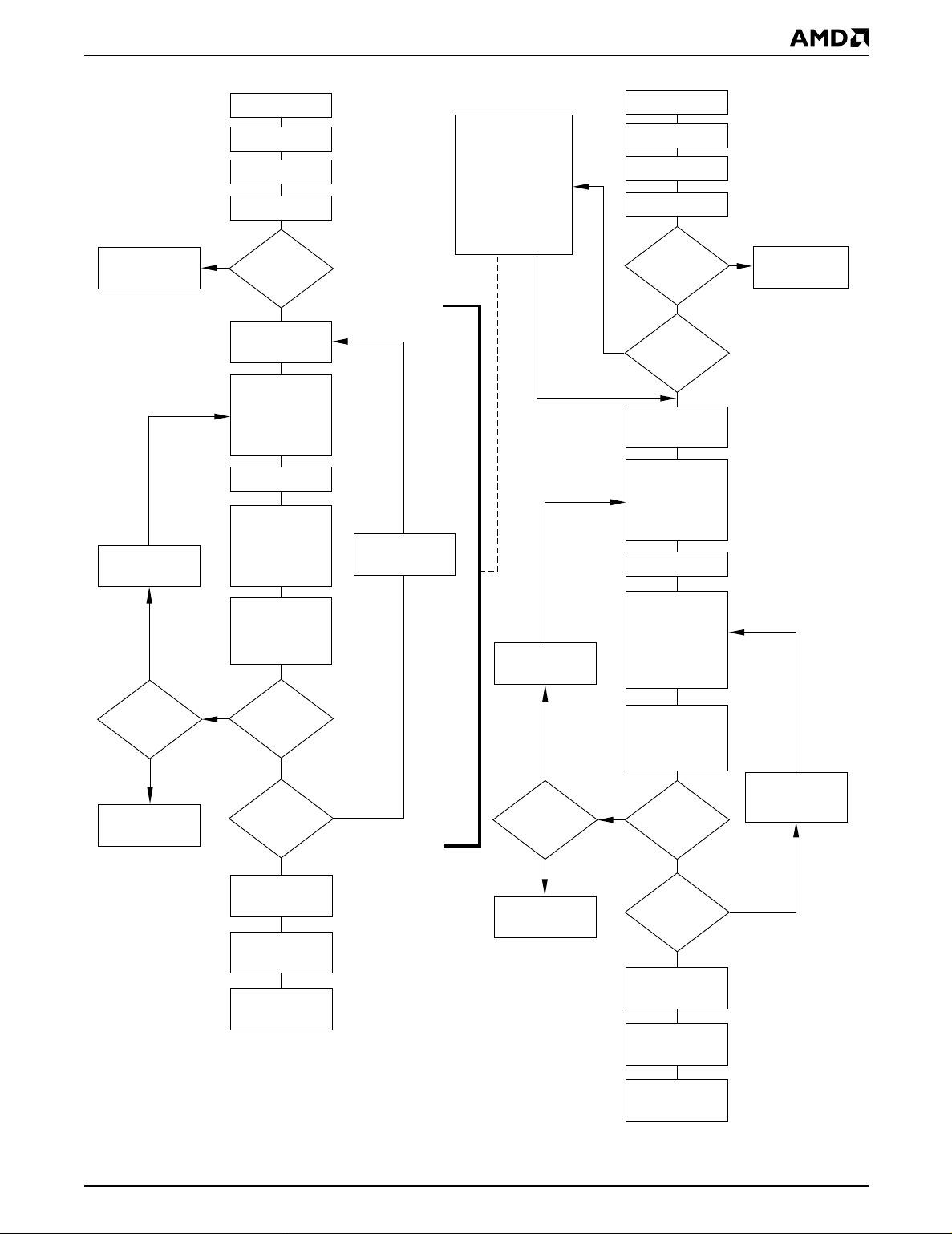
Figure 1. In-System Sector Protect/Unprotect Algorithms
Sector Protect:
Write 60h to sector
address with
A6 = 0, A1 = 1,
A0 = 0
Set up sector
address
Wait 150 µs
Verify Sector
Protect: Write 40h
to sector address
with A6 = 0,
A1 = 1, A0 = 0
Read from
sector address
with A6 = 0,
A1 = 1, A0 = 0
START
PLSCNT = 1
RESET# = V
ID
Wait 1 µs
First Write
Cycle = 60h?
Data = 01h?
Remove V
ID
from RESET#
Write reset
command
Sector Protect
complete
Yes
Yes
No
PLSCNT
= 25?
Yes
Device failed
Increment
PLSCNT
Temporary Sector
Unprotect Mode
No
Sector Unprotect:
Write 60h to sector
address with
A6 = 1, A1 = 1,
A0 = 0
Set up first sector
address
Wait 15 ms
Verify Sector
Unprotect: Write
40h to sector
address with
A6 = 1, A1 = 1,
A0 = 0
Read from
sector address
with A6 = 1,
A1 = 1, A0 = 0
START
PLSCNT = 1
RESET# = V
ID
Wait 1 µs
Data = 00h?
Last sector
verified?
Remove V
ID
from RESET#
Write reset
command
Sector Unprotect
complete
Yes
No
PLSCNT
= 1000?
Yes
Device failed
Increment
PLSCNT
Temporary Sector
Unprotect Mode
No
All sectors
protected?
Yes
Protect all sectors:
The indicated portion
of the sector protect
algorithm must be
performed for all
unprotected sectors
prior to issuing the
first sector
unprotect address
Set up
next sector
address
No
Yes
No
Yes
No
No
Yes
No
Sector Protect
Algorithm
Sector Unprotect
Algorithm
First Write
Cycle = 60h?
Protect another
sector?
Reset
PLSCNT = 1
21524B-4
12 Am29LV008B
PRELIMINARY
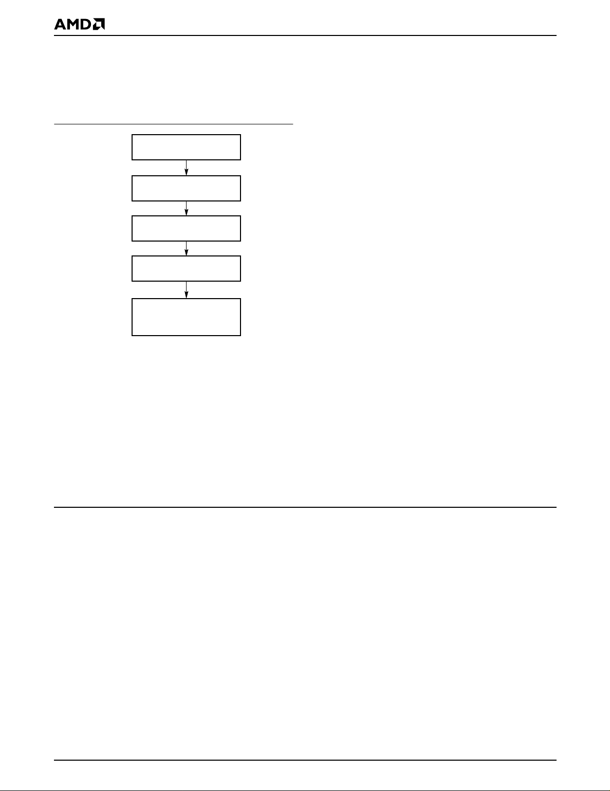
Temporary Sector Unprotect
This feature allows temporary unpr otection of previ-
ously protected sectors to change data in-system. The
Sector Unprotect mode is activated by setting the RE-
SET# pin to V
ID
. During this mode, formerly protected
sectors can be programmed or erased b y selecting the
sector addresses. Once V
ID
is removed from the RE-
SET# pin, all the previously protected sectors are
protected again. Figure 2 shows the algorithm, and
Figure 20 shows the tim ing diagrams, for this feature.
Figure 2. Temporary Sector Unprotect Operation
Hardware Data Protection
The command sequence requirement of unlock cycles
for programming or erasing provides data protection
against inadverten t writes (refer to Table 5 for com-
mand definitions). In addition, the following hardwar e
data protection mea sures prevent accidental erasure
or programming, which might otherwise be caused by
spurious system level signals during V
CC
power-up
and power-down transitions, or from system noise.
Low V
CC
Write Inhibit
When V
CC
is less than V
LKO
, the device does not ac-
cept any write cycles. This protects data during V
CC
power-up and power-down. The command register and
all internal program/erase circuits are disabled, and the
device resets. Subsequent writes are ignored until V
CC
is greater than V
LKO
. The system must provide the
proper signals to the control pins to prevent uninten-
tional writes when V
CC
is greater than V
LKO
.
Write Pulse “Glitch” Protection
Noise pulses of less than 5 ns (typical) on OE#, CE# or
WE# do not initiate a write cycle.
Logical Inhibit
Write cycles are inhibited by holding any one of OE# =
V
IL
, CE# = V
IH
or WE# = V
IH
. To initiate a write cycle,
CE# and WE# must be a logical zero while OE# is a
logical one.
Power-Up Write Inhibit
If WE# = CE# = V
IL
and OE# = V
IH
during power up , the
device does not accept commands on the rising edge
of WE#. The internal state mac hine is automatically
reset to reading array data on power-up.
COMMAND DEFINITIONS
Writing specific address and data commands or
sequences into the command register initiates device
operations. Table 5 defin es the v al i d regist er command
sequences. Writing incorrect address and data
values or writing them in the improper sequence
resets the device to reading array data.
All addresses are latched on the falling edge of WE# or
CE#, whichever happens later. All data is latched on
the rising edge of WE# or CE#, whichever happens
first. Refer to the appropriate timing diagrams in the
“AC Characteristics” section.
Reading Array Data
The device is automatically set to reading array data
after device power-up. No commands are required to
retrieve data. The device is also ready to read array
data after comp leting an Embedded Program o r
Embedded Erase algorithm.
After the device accepts an Era se Suspend command,
the device enters the Erase Suspend mode. The
system can read array data using the standard read
timings, except that if it reads at an address within
erase-suspended sectors, the device outputs status
data. After completing a program ming operation in the
Erase Suspend mode, the system may once again
read array data with the same exception. See “Erase
Suspend/Erase Resume Commands” for more infor-
mation on this mode.
The system
must
issue the reset command to re-
enable the device for reading array data if DQ5 goes
high, or while in the autoselect mode. See the “Reset
Command” section, next.
START
Perform Erase or
Program Operations
RESET# = V
IH
Temporary Sector
Unprotect Completed
(Note 2)
RESET# = V
ID
(Note 1)
Notes:
1. All protected sectors unprotected.
2. All previously protected sectors are protected once
again.
21524B-5
Loading...