


AM27C64-90DI
Table of contents
 Loading...
AMD Advanced Micro Devices AM27C64-90DI, AM27C64-90DEB, AM27C64-90DE, AM27C64-90DCB, AM27C64-90DC Datasheet
...
FINAL
Am27C64
64 Kilobit (8 K x 8-Bit) CMOS EPROM
DISTINCTIVE CHARACTERISTICS
■ Fast access time
— Speed options as fast as 45 ns
■ Low power consumption
— 20 µA typical CMOS standby current
■ JEDEC-approved pinout
■ Single +5 V power supply
■ ±10% power supply tolerance standard
■ 100% Flashrite™ programming
— Typical programming time of 1 second
GENERAL DESCRIPTION
The Am27C64 is a 64-Kbit, ultraviolet erasable programmable read-only memory. It is organized as 8K
words by 8 bits per word, operates from a single +5 V
supply, has a static standby mode, and features fast
single address location programming. Products are
available in windowed ceramic DIP packages, as well
as plastic one time programmable (OTP) PDIP and
PLCC packages.
Data can be typically accessed in less than 45 ns, allowing high-p erformance m icroproces sors to ope rate
without any WAIT states. The device offers separate
Output Enable (OE# ) and Chip Enable (CE#) controls,
■ Latch-up protected to 100 mA from –1 V to
+ 1 V
V
CC
■ High noise immunity
■ Versatile features for simple interfacing
— B oth CMOS and TTL input/output compatibility
— Two line control functions
■ Standard 28-pin DIP, PDIP, and 32-pin PLCC
packages
thus eliminating bus contention in a mul tiple bus microprocessor system.
AMD’s CMOS process technology provides high
speed, low power, and high noise immunity. Typical
power consumption is only 80 mW in active mode, and
100 µW in standby mode.
All signals are TTL levels, including programming signals. Bit locations may be programmed singly, in
blocks, or at random. The device suppor ts AMD’s
Flashrite programming alg orithm (100 µs pulses), resulting in a typical programming time of 1 second.
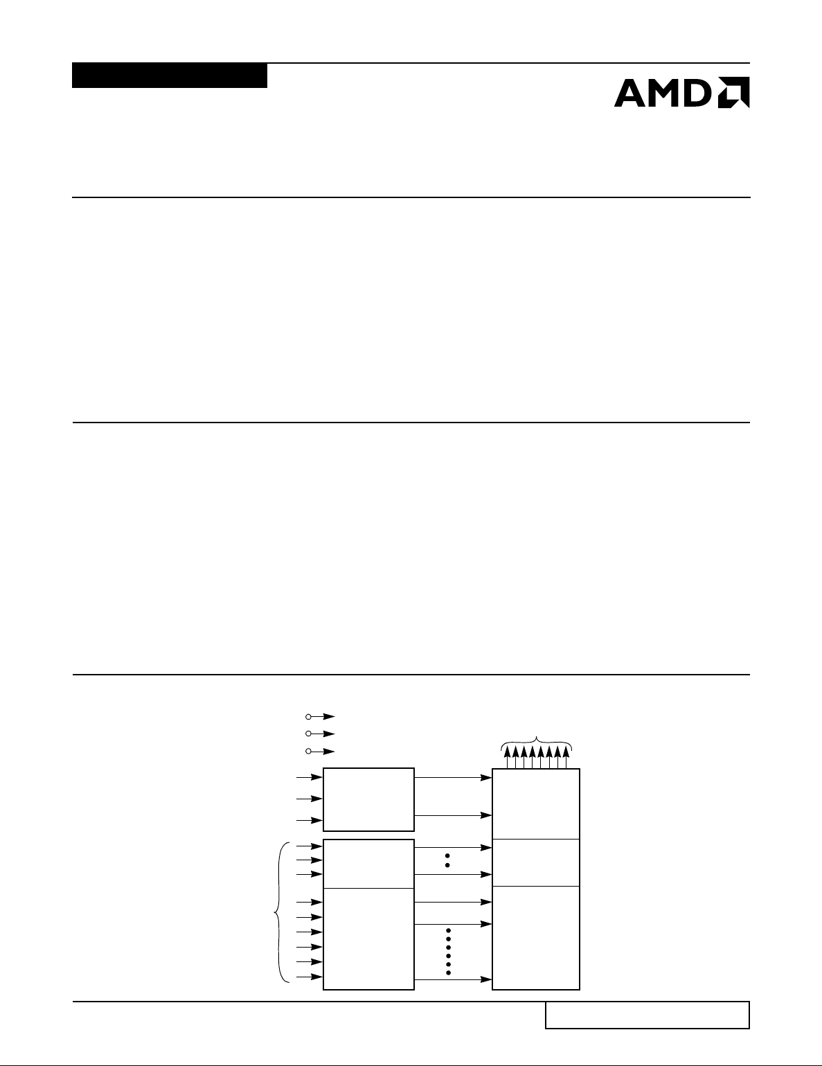
BLOCK DIAGRAM
PGM#
A0–A12
Address
Inputs
OE#
CE#
V
CC
V
SS
V
PP
Output Enable
Chip Enable
and
Prog Logic
Y
Decoder
X
Decoder
Data Outputs
DQ0–DQ7
Output
Buffers
Y
Gating
65,538
Bit Cell
Matrix
Publication# 11419 Rev: E Amendment/0
Issue Date: May 1998
11419E-1
PRODUCT SELECTOR GUIDE
Family Part Number Am27C64
= 5.0 V ± 5% -255
V
Speed Options
Max Access Time (ns) 45 55 70 90 120 150 200 250
CE# (E#) Access (ns) 45 55 70 90 120 150 200 250
OE# (G#) Access (ns) 30 35 40 40 50 50 50 50
CC
= 5.0 V ± 10% -45 -55 -70 -90 -120 -150 -200
V
CC
CONNECTION DIAGRAMS
Top View
DIP PLCC
28
27
26
25
24
23
22
21
20
19
18
17
16
15
V
CC
PGM# (P#)
NC
A8
A9
A11
OE# (G#)
A10
CE# (E#)
DQ7
DQ6
DQ5
DQ4
DQ3
11419E-2
A6
A5
A4
A3
A2
A1
A0
NC
DQ0
5
6
7
8
9
10
11
12
13
14
A7
15
DQ1
A12
DQ2
PP
CC
PGM# (P#)
DU
V
13130234
32
17
18
SS
DU
V
V
19 2016
DQ3
DQ4
NC
29
28
27
26
25
24
23
22
21
DQ5
A8
A9
A11
NC
OE# (G#)
A10
CE# (E#)
DQ7
DQ6
11419E-3
V
PP
A12
A7
A6
A5
A4
A3
A2
A1
A0
DQ0
DQ1
DQ2
V
SS
1
2
3
4
5
6
7
8
9
10
11
12
13
14
Notes:
1. JEDEC nomenclature is in parenthesis.
2. Don’t use (DU) for PLCC.
PIN DESIGNATIONS
LOGIC SYMBOL
A0–A12 = Address Inputs
CE# (E#) = Chip Enable Input
DQ0–DQ7 = Data Input/Outputs
OE# (G#) = Output Enable Input
PGM# (P#) = Program Enable Input
V
CC
V
PP
V
SS
=VCC Supply Voltage
= Program Voltage Input
= Ground
NC = No Internal Connection
2 Am27C64
13
A0–A12
CE# (E#)
PMG# (P#)
OE# (G#)
8
DQ0–DQ7
11419E-4
ORDERING INFORMATION
UV EPROM Products
AMD standard products are available in several packages and operating ranges. The order number (Valid Combination) is formed
by a combination of the following:
AM27C64 -45 D C
DEVICE NUMBER/DESCRIPTION
Am27C64
64 Kilobit (8 K x 8-Bit) CMOS UV EPROM
B
OPTIONAL PROCESSING
Blank = Standard Processing
B = Burn-In
TEMPERATURE RANGE
C = Commercial (0°C to +70
I=Industrial (–40
E = Extended (–55°C to +125°C)
PACKAGE TYPE
D = 28-Pin Ceramic DIP (CDV028)
SPEED OPTION
See Product Selector Guide and Valid Combinations
°C to +85°C)
°C)
AM27C64-45
AM27C64-55
AM27C64-70
AM27C64-90
AM27C64-120
AM27C64-150
AM27C64-200
AM27C64-255
= 5.0 V ± 5%
V
CC
Valid Combinations
DC, DCB, DI, DIB
DC, DCB, DI, DIB, DE, DEB
DC, DCB, DI, DIB
Valid Combinations
Valid Combinations list configurations planned to be supported in volume for this device. Consult the local AMD sales
office to confirm availability of specific valid combinations and
to check on newly released combinations.
Am27C64 3
ORDERING INFORMATION
OTP EPROM Products
AMD standard products are available in several packages and operating ranges. The order number (Valid Combination) is formed
by a combination of the following:
AM27C64 -55 P C
OPTIONAL PROCESSING
Blank = Standard Processing
TEMPERATURE RANGE
C = Commercial (0
I=Industrial (–40
E = Extended (–55°C to +125°C)
PACKAGE TYPE
P = 28-Pin Plastic DIP (PD 028)
J = 32-Pin Plastic Leaded Chip Carrier (PL 032)
SPEED OPTION
See Product Selector Guide and Valid Combinations
°C to +70°C)
°C to +85°C)
AM27C64-55
AM27C64-70
AM27C64-90
AM27C64-120
AM27C64-150
AM27C64-200
AM27C64-255
Valid Combinations
JC, PC, JI, PI
DEVICE NUMBER/DES CR IP TIO N
Am27C64
64 Kilobit (8 K x 8-Bit) CMOS OTP EPROM
Valid Combinations
Valid Combinations list configurations planned to be supported in volume for this device. Consult the local AMD sales
office to confirm availability of specific valid combinations and
to check on newly released combinations.
4 Am27C64
Loading...