


AM27X512-255PC
Table of contents
 Loading...
AMD Advanced Micro Devices AM27X512-255PC, AM27X512-255JI, AM27X512-255JC, AM27X512-200PI, AM27X512-200PC Datasheet
...
FINAL
Publication# 12081 Rev: F Amendment/0
Issue Date: May 1998
Am27X512
512 Kilobit (64 K x 8-Bit) CMOS ExpressROM Device
DISTINCTIVE CHARACTERISTICS
■ As an OTP EPROM alternative:
— Factory optimized programming
— Fully tested and guaranteed
■ As a Mask ROM alternative:
— Shorter leadtime
— Lower volume per code
■ Fast access time
— 70 ns
■ Single +5 V power supply
■ Compatible wit h JEDEC-approved EPROM
pinout
■ ±10% power supply tolerance
■ High noise immunity
■ Low power dissipation
— 100 µA maximum CMOS standby current
■ Av ailable in Plastic Dual-In-line Pac kage (PDIP)
and Plastic Leaded Chip Carrier (PLCC)
■ Latch-up protected to 100 mA from –1 V to
V
CC
+ 1 V
■ Versatile features for simple interfacing
— Both CMOS and TTL input/output compatibility
— Two line control functions
GENERAL DESCRIPTION
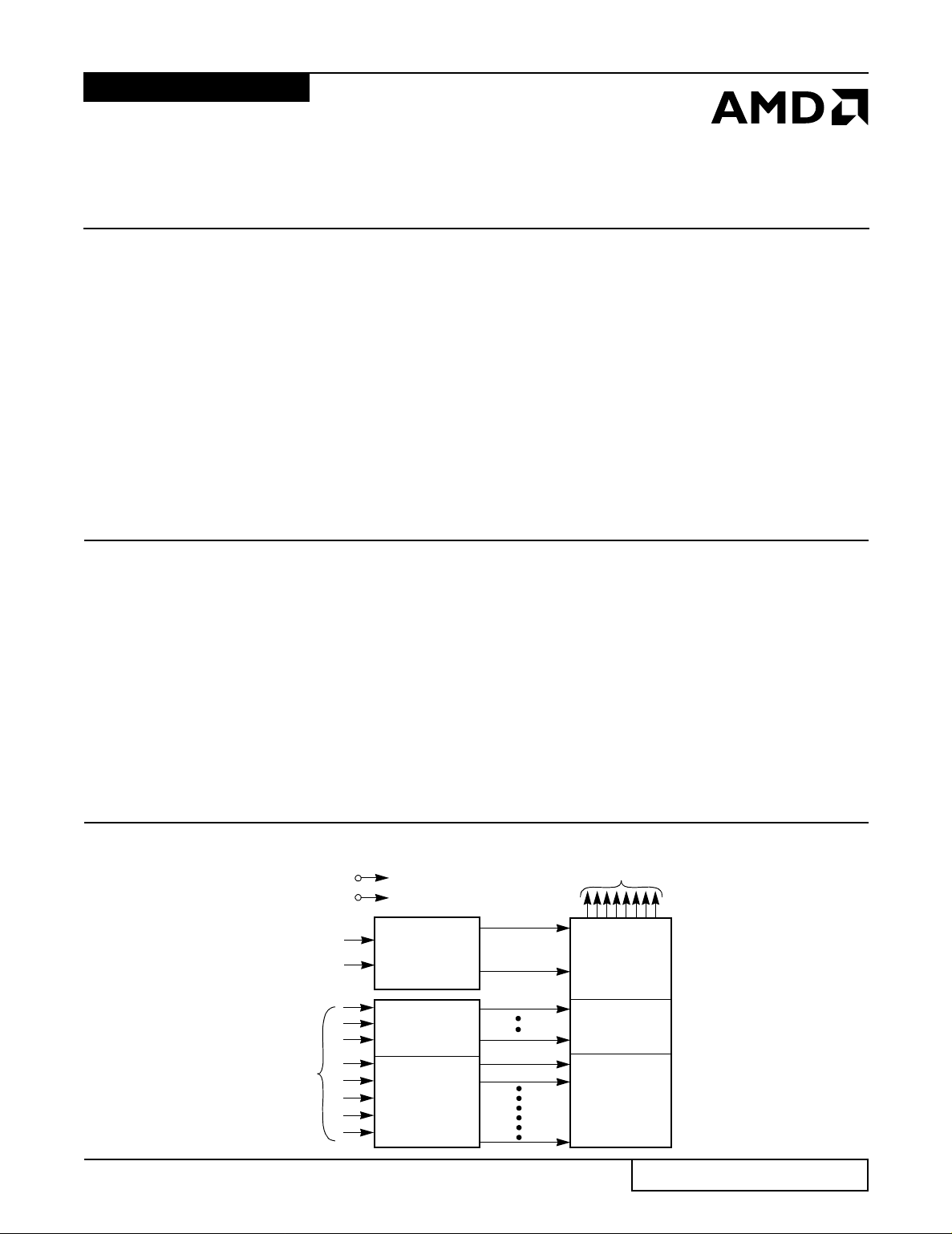
The Am27X512 is a factory programmed and tested
OTP EPROM. It is progra mmed after pac kaging prior to
final test. Every device is rigorously tested under AC
and DC operating conditions to your stable code. It is
organized as 64 Kwords by 8 bits per word and is av ail-
able in plastic dual in-line packages (PDIP), as well as
plastic leaded chip carrier (PLCC) packages. Express-
ROM devices provide a board-ready memory solution
for medium to high volume codes with short leadtimes.
This offers manufacturers a cost-effective and flexible
alternative to OTP EPROMs and mask programmed
ROMs.
Data can be accessed as fast as 70 ns, allowing
high-performance microprocessors to operate with re-
duced WAIT states. The device offers separate Output
Enable (OE#) and Chip Enable (CE#) controls, thus
eliminating bus contention in a multiple bus micropro-
cessor system.
AMD’s CMOS process technology provides high
speed, low power, and high noise immunity. Typical
power consumption is only 80 mW in active mode, and
100 µW in standby mode.
BLOCK DIAGRAM
12081F-1
A0–A15
Address
Inputs
CE#
OE#
V
CC
V
SS
Data Outputs DQ0–DQ7
Output
Buffers
Y
Gating
524,288
Bit Cell
Matrix
X
Decoder
Y
Decoder
Output Enable
Chip Enable
and
Prog Logic
2 Am27X512
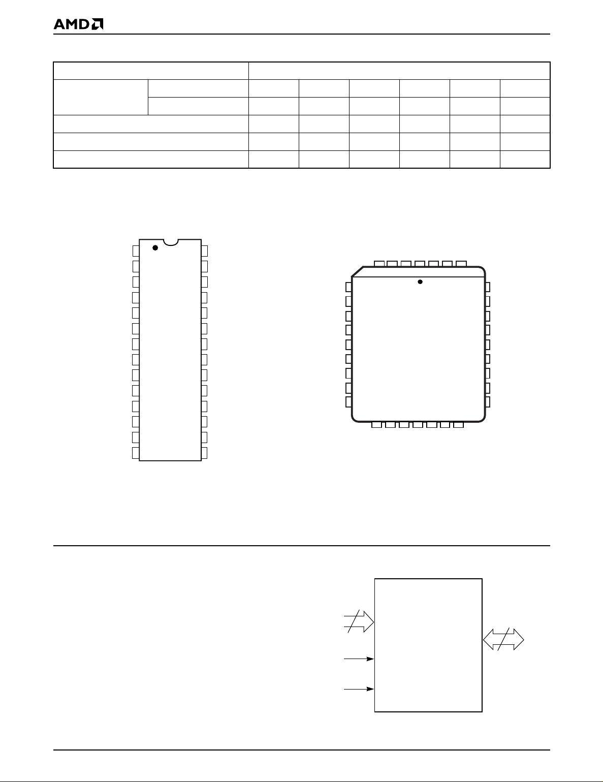
PRODUCT SELECTOR GUIDE
CONNECTION DIAGRAMS
Top View
DIP PLCC
Notes:
1. JEDEC nomenclature is in parenthesis.
2. Don’t use (DU) for PLCC.
PIN DESIGNATIONS
A0–A15 = Address Inputs
CE# (E#) = Chip Enable Input
DQ0–DQ7 = Data Input/Outputs
OE# (G#) = Output Enable Input
PGM# (P#) = Program Enable Input
V
CC
=V
CC
Supply Voltage
V
PP
= Program Voltage Input
V
SS
= Ground
NC = No Internal Connection
LOGIC SYMBOL
Family Part Number Am27X512
Speed Options
V
CC
= 5.0 V ± 5% -255
V
CC
= 5.0 V ± 10% -70 -90 -120 -150 -200
Max Access Time (ns) 70 90 120 150 200 250
CE# (E#) Access (ns) 70 90 120 150 200 250
OE# (G#) Access (ns) 70 40 50 65 75 100
3
4
5
2
1
9
10
11
12
13
23
22
21
20
19
7
8
18
17
6
28
27
16
14
26
25
24
15
A6
A5
A4
A3
A2
A1
A0
DQ0
A7
DQ1
DQ2
V
SS
A8
A9
A11
OE# (G#)/V
PP
A10
CE# (E#)
DQ7
V
CC
A14
DQ6
A13
DQ5
DQ4
DQ3
A15
A12
12081F-2
DQ5
DU
DQ4
DQ3
DU
13130234
5
6
7
8
9
10
11
12
13
17
18
19 2016
15
14
29
28
27
26
25
24
23
22
21
32
A6
A5
A4
A3
A2
A1
A0
NC
DQ0
A8
A9
A11
NC
OE# (G#)/V
PP
A10
CE# (E#)
DQ7
DQ6
A7
A12
A15
V
CC
A14
A13
DQ1
DQ2
V
SS
12081F-3
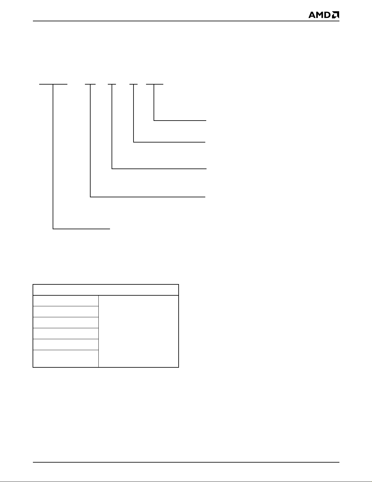
16
8
DQ0–DQ7
A0–A15
CE# (E#)
OE# (G#)
12081F-4
Am27X512 3
ORDERING INFORMATION
Standard Pr od ucts
AMD standard products are available in several packages and operating ranges. The order number (Valid Combination) is formed
by a combination of the following:
Valid Combinations
Valid Combinations list configurations planned to be sup-
ported in volume for this device. Consult the local AMD sales
office to confirm availability of specific valid combinations and
to check on newly released combinations.
DEVICE NUMBER/DESCRIPTION
Am27X512
512 Kilobit (64 K x 8-Bit) CMOS ExpressROM Device
AM27X512
-70 J C
CODE DESIGNATION
Assigned by AMD
TEMPERATURE RANGE
C = Commercial (0°C to +70
°C)
I=Industrial (–40
°C to +85°C)
PACKAGE TYPE
P = 28-Pin Plastic Dual In-Line Package (PD 028)
J = 32-Pin Plastic Leaded Chip Carrier (PL 032)
SPEED OPTION
See Product Selector Guide and Valid Combinations
XXXXX
Valid Combinations
AM27X512-70
PC, JC, PI, JI
AM27X512-90
AM27X512-120
AM27X512-150
AM27X512-200
AM27X512-255
V
CC
= 5.0 V ± 5%
Loading...