


AM29SL800BB-200ECB
AMD Advanced Micro Devices AM29SL800BB-200ECB, AM29SL800BB-200EC, AM29SL800B, AM29SL800BT, AM29SL800BT-200WBCB Datasheet
...
ADVANCE INFORMATION
This document contains information on a product under development at Advanced Micro Devices. The information
is intended to help you ev aluate this product. AMD reserves the right to change or dis continue work on thi s proposed
product without notice.
Publication# 21545 Rev: A Amendment/+2
Issue Date: March 1998
Refer to AMD’s Website (www.amd.com) for the latest information.
Am29SL800B
8 Megabit (1 M x 8-Bit/512 K x 16-Bit)
CMOS 1.8 Volt-only Super Low Voltage Flash Memory
DISTINCTIVE CHARACTERISTICS
■ Single power supply operation
— 1.8 to 2.2 V for read, program, and erase
operations
— Ideal for battery-powered applications
■ Manufactured on 0.35 µm process technology
■ High performance
— Access times as fast as 170 ns
■ Ultra low power consumption (typical values at
5 MHz)
— 65 nA Automatic Sleep Mode current
— 65 nA standby mode current
— 5 mA read current
— 10 mA program/erase current
■ Flexible sector architecture
— One 16 Kbyte, two 8 Kbyte, one 32 Kbyte, and
fifteen 64 Kbyte sectors (byte mode)
— One 8 Kword, two 4 Kword, one 16 Kword, and
fifteen 32 Kword sectors (word mode)
— Supports full chip erase
— Sector Protection features:
A hardware method of locking a sector to
prevent any program or erase operations within
that sector
Sectors can be locked in-system or via
programming equipment
T emporary Sector Unprotect feat ure allows code
changes in previously locked sectors
■ Unlock Bypass Program Command
— Reduces overall progr amming time when
issuing multiple program command sequences
■ Top or bottom boot block configurations
available
■ Embedded Al gorithms
— Embedded Erase algorithm automatically
preprograms and erases the entire chip or any
combination of designated sectors
— Embedded Program algorithm automatically
writes and verifies data at specified addresses
■ Minimum 1,000,000 write cycle guarantee per
sector
■ Package option
— 48-pin TSOP
— 48-ball FBGA
■ Compatibility with JEDEC standards
— Pinout and software compatible with single-
power supply Flash
— Superior inadvertent write protection
■ Data# Polling and toggle bits
— Provides a software method of detecting
program or erase operation completion
■ Ready/Busy# pin (RY/BY#)
— Provides a hardware method of detecting
program or erase cycle completion
■ Erase Suspend/Erase Resume
— Suspends an erase operati on to read dat a from,
or program data to, a sector that is not being
erased, then resumes the erase operation
■ Hardware reset pin (RESET#)
— Hardware method to reset the de vice t o reading
array data

2 Am29SL800B
ADVANCE INFORMATION
GENERAL DESCRIPTION
The Am29SL800B is an 8 Mbit, 1.8 V volt-only Flash
memory organized as 1,048,576 bytes or 524,288
words. The device is offered in 48-pin TSOP and 48ball FBGA packages. The word-wide data (x16)
appears on DQ 15–DQ0; the byte-wide (x8) data
appears on DQ7–DQ0. This device is designed to be
programmed and erased in-system with a single 1.8
volt V
CC
supply. No VPP is for write or erase operations.
The device can also be programmed in standard
EPROM programmers.
The standard device offers access times of 170 or 200
ns, allowing high speed microp rocessors to operate
without wait states. To eliminate bus contention the
device has separate chip enable (CE#), write enable
(WE#) and output enable (OE#) controls.
The device requires only a single 1. 8 v o lt po wer sup-
ply for both read and write functions. Internally generated and regulated voltages are provided for the
program and erase operations.
The device is entirely command set compatible with the
JEDEC single-power-supply Flash standard. Commands are written to the command regis ter using
standard micropr ocessor wri te timings. Register co ntents serve as input to an internal state-machine that
controls the erase and programming circuitry. Write
cycles also internally latch addresses and data needed
for the programming and erase operations. Reading
data out of the device is similar to reading from other
Flash or EPROM devices.
Device programming occurs by executing the program
command sequence. This initiates the Embedded
Program algorithm—an internal algorithm that automatically times the program pulse widths and verifies
proper cell margin. The Unlock Bypass mode facilitates faster programming times by requir ing only two
write cycles to program data instead of four.
Device erasure occurs by ex ecuting the erase command
sequence. This initiates the Embedded Erase algorithm—an i nternal algorithm that autom atically prepro grams the array (if it is not already programmed) before
executing the erase operation. During erase, the device
automatically times the erase pulse widths and verifies
proper cell margin.
The host system can detect whether a program or
erase operation is complete by observing the RY/BY#
pin, or by reading the DQ7 (Data# Polling) and DQ6
(toggle) status bits. After a program or erase cycle
has been completed, the device is ready to read array
data or accept another command.
The sector erase ar chitecture allo ws memo ry secto rs
to be erased and reprogrammed without affecting the
data contents of other sectors. The device is fully
erased when shipped from the factory.
Hardware data protection measures include a low
V
CC
detector that automatically in hibits write operations during power transitions. The hardware sector
protection feature disables both program and erase
operations in any combination of the sectors of memory. This can be achieved in-system or via programming equipment.
The Erase Suspend feature enables the user to put
erase on hold for any period of time to read data from,
or program data to, any sector that is not selected for
erasure. True background erase can thus be achieved.
The hardware RESET# pi n terminates any operation
in progress and resets the internal state machine to
reading array dat a. The RESET# pin ma y be tied to the
system reset circuitry. A system reset would thus also
reset the device, enabling the system microprocessor
to read the boot-up firmware from the Flash memory.
The device offers two power-saving features. When
addresses have been stable for a specified amount of
time, the device enters the automatic sleep m ode.
The system can also place the de vice into the standby
mode. Power consumption is greatly reduced in both
these modes.
AMD’s Flash technology combines years of Flash
memory manufacturing experience to produce the
highest levels of quality, reliability and cost effectiveness. The device electrically erases all bits within
a sector simultaneously via Fowler-Nordheim tunneling. The data is programmed using hot electron
injection.
Am29SL800B 3
ADVANCE INFORMATION
PRODUCT SELECTOR GUIDE
Note: See “AC Characteristics” for full specifications.
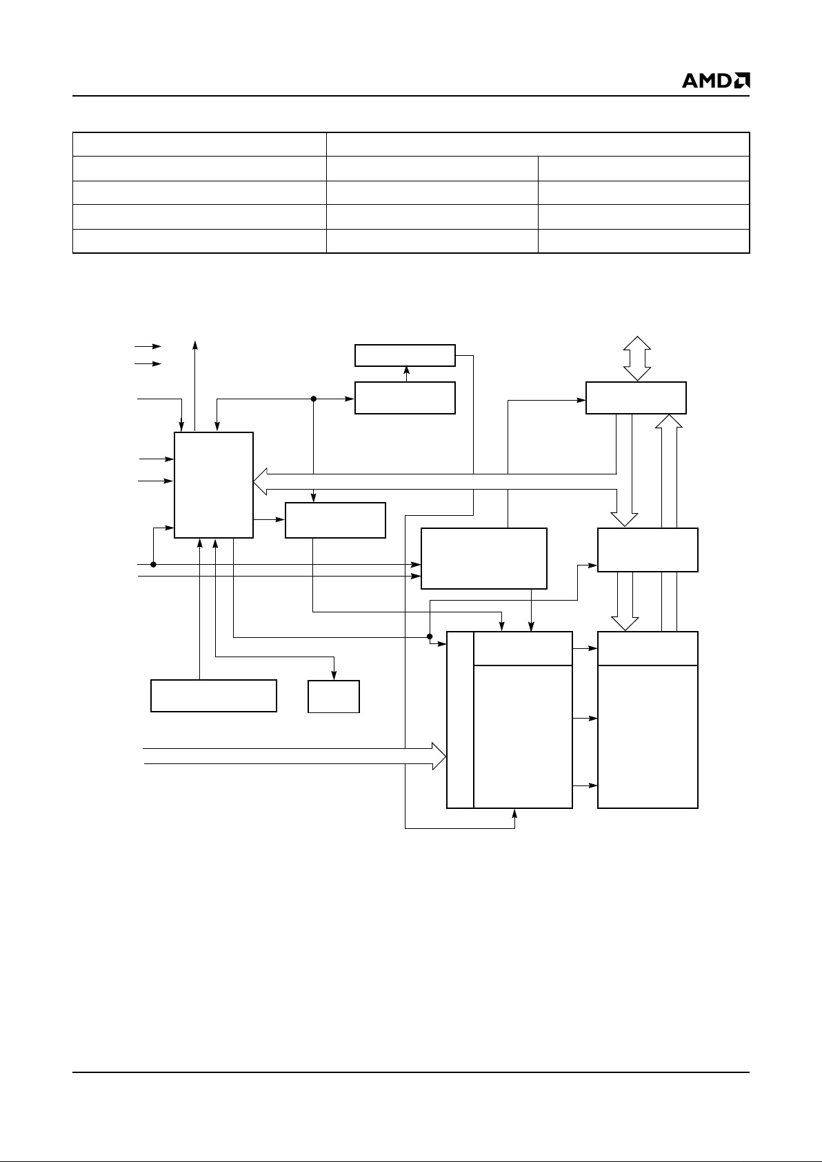
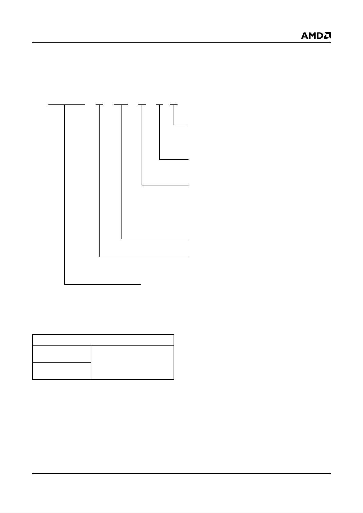
BLOCK DIAGRAM
Family Part Number Am29SL800B
Speed Options 170 200
Max access time, ns (t
ACC
) 170 200
Max CE# access time, ns (tCE) 170 200
Max OE# access time, ns (tOE) 90 90
Input/Output
Buffers
X-Decoder
Y-Decoder
Chip Enable
Output Enable
Logic
Erase Voltage
Generator
PGM Voltage
Generator
Timer
VCC Detector
State
Control
Command
Register
V
CC
V
SS
WE#
BYTE#
CE#
OE#
STB
STB
DQ0
–
DQ15 (A-1)
Sector Switches
RY/BY#
RESET#
Data
Latch
Y-Gating
Cell Matrix
Address Latch
A0–A18
21545A-1
4 Am29SL800B
ADVANCE INFORMATION
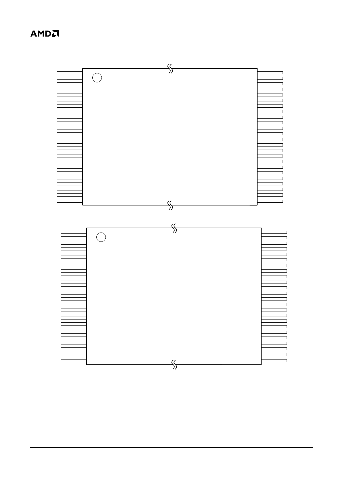
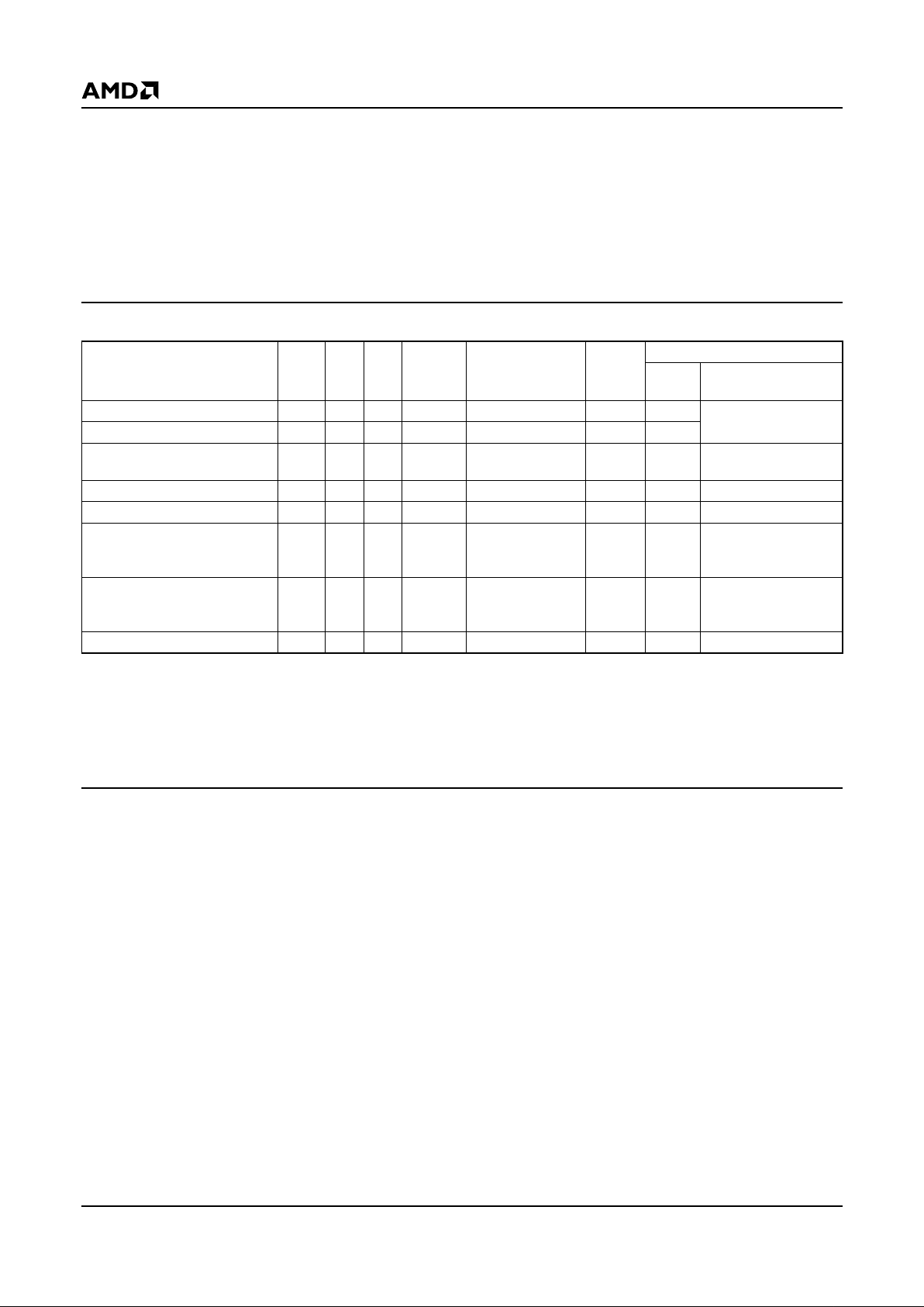
CONNECTION DIAGRAMS
A1
A15
A18
A14
A13
A12
A11
A10
A9
A8
NC
NC
WE#
RESET#
NC
NC
RY/BY#
A17
A7
A6
A5
A4
A3
A2
1
16
2
3
4
5
6
7
8
17
18
19
20
21
22
23
24
9
10
11
12
13
14
15
A16
DQ2
BYTE#
V
SS
DQ15/A-1
DQ7
DQ14
DQ6
DQ13
DQ9
DQ1
DQ8
DQ0
OE#
V
SS
CE#
A0
DQ5
DQ12
DQ4
V
CC
DQ11
DQ3
DQ10
48
33
47
46
45
44
43
42
41
40
39
38
37
36
35
34
25
32
31
30
29
28
27
26
21545A-2
Reverse TSOP
Standard TSOP
Am29SL800B 5
ADVANCE INFORMATION
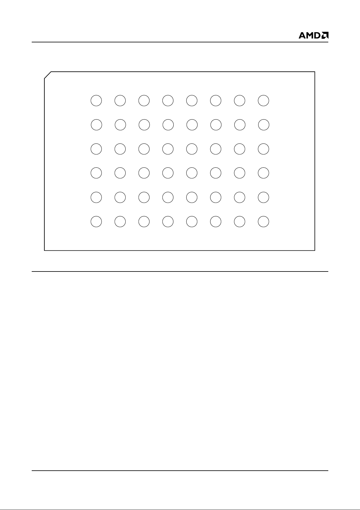
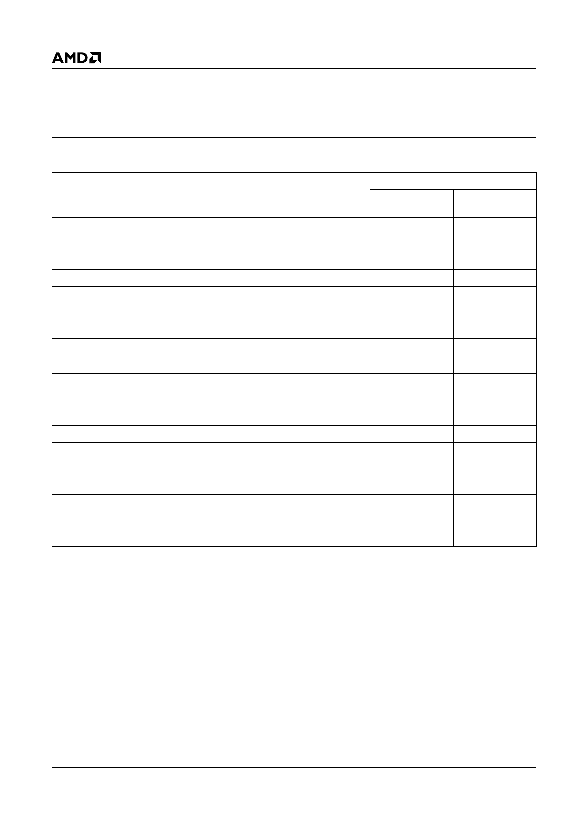
CONNECTION DIAGRAMS
Special Handling Instructions for FBGA
Packages
Special handling is required for Flash Memory products
in FBGA packages.
Flash memory devices in FBGA packages may be
damaged if exposed to ultrasonic cleaning methods.
The package and/or data integrity may be compromised
if the package body is exposed to temperatures above
150°C for prolonged periods of time.
A1 B1 C1 D1 E1 F1 G1 H1
A2 B2 C2 D2 E2 F2 G2 H2
A3 B3 C3 D3 E3 F3 G3 H3
A4 B4 C4 D4 E4 F4 G4 H4
A5 B5 C5 D5 E5 F5 G5 H5
A6 B6 C6 D6 E6 F6 G6 H6
DQ15/A-1 V
SS
BYTE#A16A15A14A12A13
DQ13 DQ6DQ14DQ7A11A10A8A9
V
CC
DQ4DQ12DQ5NCNCRESET#WE#
DQ11 DQ3DQ10DQ2NCA18NCRY/BY#
DQ9 DQ1DQ8DQ0A5A6A17A7
OE# V
SS
CE#A0A1A2A4A3
21545A-3
48-Ball FBGA (Bottom View)
6 Am29SL800B
ADVANCE INFORMATION
PIN CONFIGURATION
A0–A18 = 19 addresses
DQ0–DQ14 = 15 data inputs/outputs
DQ15/A-1 = DQ15 (data inp ut/ output, word mode),
A-1 (LSB address input, byte mode)
BYTE# = Selects 8-bit or 16-bit mode
CE# = Chip enable
OE# = Output enable
WE# = Write enable
RESET# = Hardwa r e reset pin, active low
RY/BY# = Ready/Busy# output
V
CC
= 1.8–2 .2 V single power supply
V
SS
= Device ground
NC = Pin not connected internally
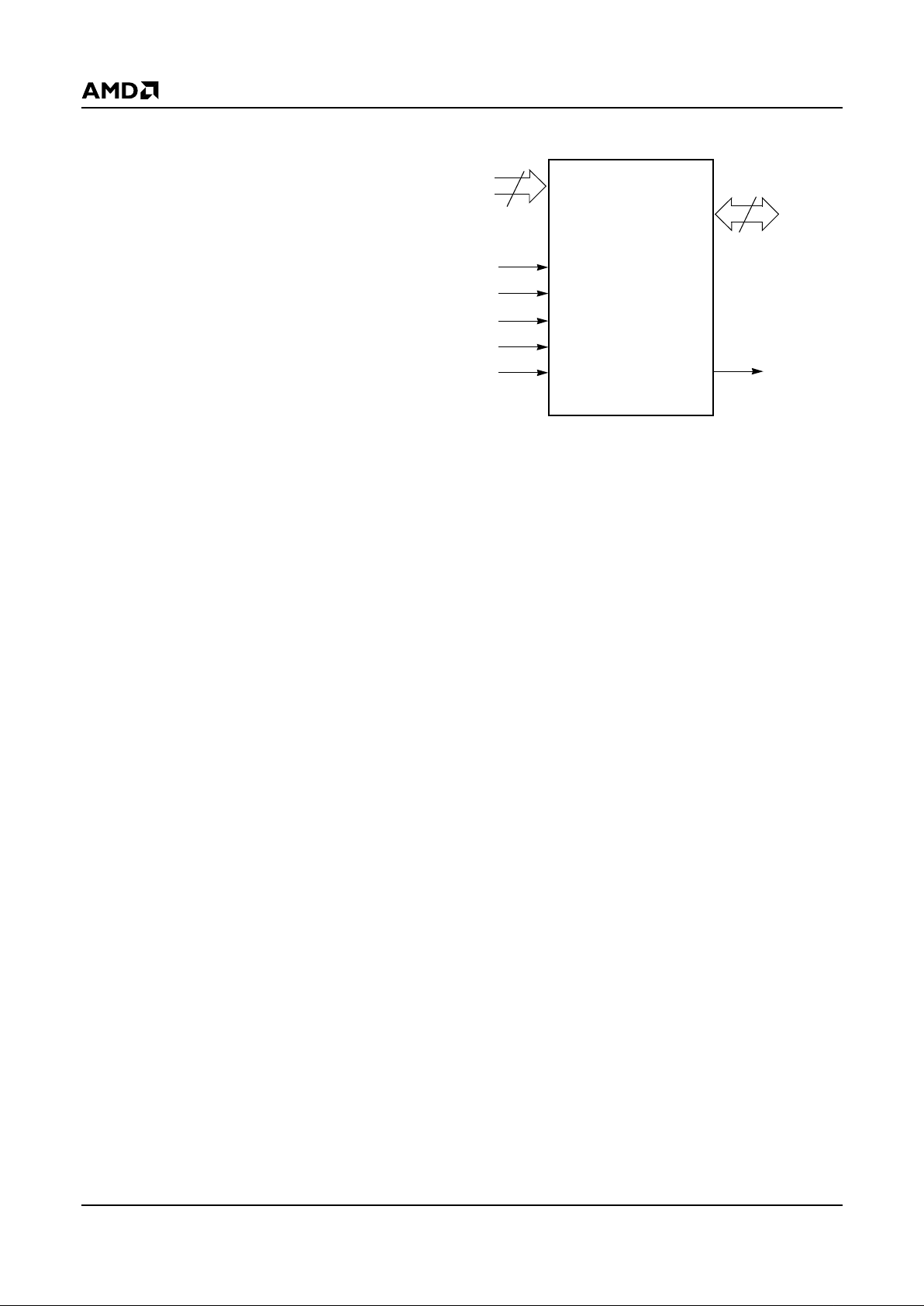
LOGIC SYMBOL
21545A-4
19
16 or 8
DQ0–DQ15
(A-1)
A0–A18
CE#
OE#
WE#
RESET#
BYTE# RY/BY#
Am29SL800B 7
ADVANCE INFORMATION
ORDERING INFORMATION
Standard Pr od ucts
AMD standard products are available in several packages and operating ranges. The order number (Valid Combination) is formed by a combination of the elements below.
Valid Combinations
Valid Combinations list configurations planned to be supported in volume for this device. Consult the local AMD sales
office to confirm availability of specific valid combinations and
to check on newly released combinations.
DEVICE NUMBER/DESCRIPTION
Am29SL800B
8 Megabit (1 M x 8-Bit/512 K x 16-Bit) CMOS Flash Memory
1.8 Volt-only Read, Program, and Erase
CE170Am29SL800B T
OPTIONAL PROCESSING
Blank = Standard Processing
B = Burn-in
(Contact an AMD representative for more information)
TEMPERATURE RANGE
C=Commercial (0°C to +70°C)
I = Industrial (–40°C to +85°C)
PACKAGE TYPE
E = 48-Pin Thin Small Outline Package (TSOP)
Standard Pinout (TS 048)
F = 48-Pin Thin Small Outline Package (TSOP)
Reverse Pinout (TSR048)
WB = 48-ball Fine-Pitch Ball Grid Array (FBGA)
0.80 mm pitch, 6 x 9 mm package
SPEED OPTION
See Product Selector Guide and Valid Combinations
BOOT CODE SECTOR ARCHITECTURE
T = Top Sector
B = Bottom Sector
Valid Combinations
Am29SL800BT170,
Am29SL800BB170
EC, EI, FC, FI, WBC, WBI
Am29SL800BT200,
Am29SL800BB200
8 Am29SL800B
ADVANCE INFORMATION
DEVICE BUS OPERATIONS
This section describes the requirements and use of the
device bus operations, which are initiated through the
internal command register. The command register itself
does not occupy any addressable memory loc ation.
The register is composed of latches that store the commands, along with the address and data information
needed to execute the command. The contents of the
register serve as inputs to the internal state machine.
The state machine outputs d ictate the function of the
device. Table 1 lists the device bus operations, the inputs and control levels they require, and the resulting
output. The following subsections describe each of
these operations in further detail.
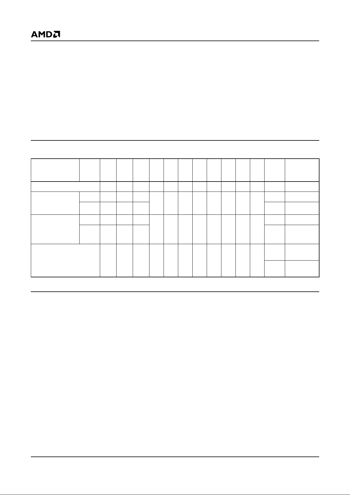
Table 1. Am29SL800B Device Bus Operations
Legend:
L = Logic Low = V
IL
, H = Logic High = VIH, VID = 10 ± 1.0 V, X = Don’t Care, AIN = Address In, DIN = Data In, D
OUT
= Data Out
Notes:
1. Addresses are A18:A0 in word mode (BYTE# = V
IH
), A18:A-1 in byte mode (BYTE# = VIL).
2. The sector protect and sector unprotect functions may also be implemented via programming equipment. See the “Sector
Protection/Unprotection” section.
Word/Byte Configuration
The BYTE# pin controls whether the device data I/O
pins DQ15–DQ0 operate in the by te or word configur ation. If the BYTE# pin is set at logic ‘1’, the device is in
word configuration, DQ15–DQ0 are activ e and c ontrolled by CE# and OE#.
If the BYTE# pin is set at logic ‘0’, the device is in byte
configuration, and only data I/O pins DQ0–DQ7 are active and controlled by CE# and OE#. The data I/O pins
DQ8–DQ14 are tri-stated, and the DQ15 pin is used as
an input for the LSB (A-1) address function.
Requirements for Reading Array Data
To read array data from the outputs, the system must
drive the CE# and OE# pins to V
IL
. CE# is the power
control and selects the device. OE# is the output control and gates array data to the output pins. WE#
should remain at V
IH
. The BYTE# pin determines
whether the device outputs array data in words or
bytes.
The internal state machine is set for reading array
data upon device po wer-u p , or after a hardw are res et.
This ensure s that no sp urious alteration of the memory content occurs dur ing the power transition. No
command is nece ssary in this mode to ob tain array
data. Standard microprocessor read cycles that assert valid addresses on the de vice addr ess inputs produce valid data on the device data outputs. The
device remains enab led f or read access until t he command register contents are altered.
See “Reading Array Data” for more information. Refer
to the AC Read Operations table for timing specifications and to Figure 13 for the timing diagram. I
CC1
in
the DC Characteristics table represents the active current specification for reading array data.
Operation CE# OE# WE# RESET#
Addresses
(Note 1)
DQ0–
DQ7
DQ8–DQ15
BYTE#
= V
IH
BYTE#
= V
IL
Read L L H H A
IN
D
OUT
D
OUT
DQ8–DQ14 = High-Z,
DQ15 = A-1
Write L H L H A
IN
D
IN
D
IN
Standby
V
CC
±
0.3 V
XX
VCC ±
0.3 V
X High-Z High-Z High-Z
Output Disable L H H H X High-Z High-Z High-Z
Reset X X X L X High-Z High-Z High-Z
Sector Protect (Note 2) L H L V
ID
Sector Address,
A6 = L, A1 = H,
A0 = L
D
IN
XX
Sector Unprotect (Note 2) L H L V
ID
Sector Address,
A6 = H, A1 = H,
A0 = L
D
IN
XX
Temporary Sector Unprotect X X X V
ID
A
IN
D
IN
D
IN
High-Z

Am29SL800B 9
ADVANCE INFORMATION
Writing Commands/Command Sequences
To write a command or command sequence (which includes programming data to the device and erasing
sectors of memory), the system must drive WE# and
CE# to V
IL
, and OE# to VIH.
For progr am operations , the BYTE# pin determines whether
the device accept s progr am data in by tes or words . Ref er to
“Word/Byte Confi gurat ion” f or more inf ormation.
The device features an Unlock Bypass mode to facili-
tate faster programming. Once the device enters the Unlock Bypass mode, only two write cycles are required to
program a word or byte, instead of four. The “Word/Byte
Program Command Sequence” section has details on
programming data to the device using both standard and
Unlock Bypass command sequences.
An erase operation can erase one sect or, multiple sectors, or the entire device. Tables 2 and 3 indicate the
address space that each sector occupies. A “sector address” consists of the addres s bits required t o un iquely
select a sector. The “Command Definitions” section
has details on erasing a sector or the entire chip, or
suspending/resuming the erase operation.
After the system writes the autoselect command sequence, the device enters the autoselect mode. The
system can then read autoselect codes from the internal register (which is separate from the memory array)
on DQ7–DQ0. Standard read cycle timings apply in this
mode. Refer to the Autoselect Mode and Autoselect
Command Sequence sections for more information.
I
CC2
in the DC Characteristics table represents the active current specification for the w rite mode. The “AC
Characteristics” section contains timing specification
tables and timing diagrams for write operations.
Program and Erase Operation Status
During an erase or program operation, the system ma y
check the status of the operation by reading the status
bits on DQ7–DQ0. Standard read cycle timings and I
CC
read specifications apply. Refer to “Write Operation
Status” for more information, and to “AC Characteristics” for timing diagrams.
Standby Mode
When the system is not reading or writing to the device, it can place the device in the standby mode. In
this mode, current consumption is greatly reduced,
and the outputs are placed in the high impedance
state, independent of the OE# input.
The device enters the CMOS standby mode when the
CE# and RESET# pin s are both held at V
CC
± 0.3 V.
(Note that this is a more restricted voltage range than
V
IH
.) If CE# and RESET# ar e held a t VIH, but not within
V
CC
± 0.3 V, the device will be in the standby mode, b ut
the standby current will be greater. The device requires
standard access time (t
CE
) for read access when the
device is in either of these standby modes, before it is
ready to read data.
The device also enters the standb y mode when the RESET# pin is driven low. Refer to the next section, RESET#: Hardware Reset Pin.
If the device is deselected during erasure or programming, the device draws active current until the
operation is completed.
I
CC3
in the DC Characteristics table represents the
standby current specification.
Automatic Sleep Mode
The automatic sleep mode minimizes Flash device
energy consumption. The device automatically
enables this mode when addres ses remain stable for
t
ACC
+ 50 ns. The automatic sleep mode is
independent of the CE#, WE#, and OE# control
signals. Standard address access timings provide new
data when addresses are chan ged. While in sleep
mode, output data is latched and always available to
the system. I
CC4
in the DC Characteristics table
represents the automatic sleep mode current
specification.
RESET#: Hardware Reset Pin
The RESET# pin provides a hardw are method of resetting the device to reading array data. When the RESET# pin is driven low for at least a period of t
RP
, the
device immediately terminates any operation in
progress, tristates all output pins, and ignores all
read/write commands for the duration of the RESET#
pulse. The device also resets the inter nal state machine to reading array data. The operation that was interrupted should be reinitiated once the device is ready
to accept another command sequence, to ensure data
integrity.
Current is reduced for the duration of the RESET#
pulse. When RESET# is held at V
SS
±0.3 V, the device
draws CMOS standby c urrent (I
CC4
). If RESET# is held
at V
IL
but not within VSS±0.3 V, the standby current will
be greater.
The RESET# pin may be tied to the system reset cir-
cuitry. A system reset would thus also reset the Flash
memory, enabling the system to read the boot-up
firmware from the Flash memory.
If RESET# is asserted during a program or erase operation, the RY/BY# pin remains a “0” (busy) until the
internal reset operation is complete, which requires a
time of t
READY
(during Embedded Algorithms). The
system can thus monitor RY/BY# to determine
whether the reset oper ation is c omplete . If RESE T# is
asserted when a program or erase oper ation is not e xecuting (RY/BY# pin is “1”), the reset operation is
completed within a time of t
READY
(not during Embed-
10 Am29SL800B
ADVANCE INFORMATION
ded Algorithms). The system can read data tRH after
the RESET# pin returns to V
IH
.
Refer to the AC Characteristics tables for RESET# parameters and to Figure 14 for the timing diagram.
Output Disable Mode
When the OE# input is at VIH, output from the device is
disabled. The output pins are placed in t he high impedance state.
Table 2. Am29SL800BT T op Boot Block Sector Address Table
Sector A18 A17 A16 A15 A14 A13 A12
Sector Size
(Kbytes/
Kwords)
Address Range (in hexadecim al )
(x8)
Address Range
(x16)
Address Range
SA00000XXX 64/32 00000h–0FFFFh 00000h–07FFFh
SA10001XXX 64/32 10000h–1FFFFh08000h–0FFFFh
SA20010XXX 64/32 20000h–2FFFFh10000h–17FFFh
SA30011XXX 64/32 30000h–3FFFFh18000h–1FFFFh
SA40100XXX 64/32 40000h–4FFFFh20000h–27FFFh
SA50101XXX 64/32 50000h–5FFFFh28000h–2FFFFh
SA60110XXX 64/32 60000h–6FFFFh30000h–37FFFh
SA70111XXX 64/32 70000h–7FFFFh38000h–3FFFFh
SA81000XXX 64/32 80000h–8FFFFh40000h–47FFFh
SA91001XXX 64/32 90000h–9FFFFh48000h–4FFFFh
SA101010XXX 64/32 A0000h–AFFFFh50000h–57FFFh
SA111011XXX 64/32 B0000h–BFFFFh58000h–5FFFFh
SA121100XXX 64/32C0000h–CFFFFh60000h–67FFFh
SA131101XXX 64/32D0000h–DFFFFh68000h–6FFFFh
SA141110XXX 64/32 E0000h–EFFFFh70000h–77FFFh
SA1511110XX 32/16 F0000h–F7FFFh78000h–7BFFFh
SA161111100 8/4 F8000h–F9FFFh7C000h–7CFFFh
SA171111101 8/4 FA000h–FBFFFh7D000h–7DFFFh
SA18111111X 16/8 FC000h–FFFFFh7E000h–7FFFFh
Am29SL800B 11
ADVANCE INFORMATION
Table 3. Am29SL800BB Bottom Boot Block Sector Address Table
Note for Tables 2 and 3: Address range is A18:A-1 in byte mode and A18:A0 in word mode. See “Word/Byte Configuration”
section for more information.
Sector A18 A17 A16 A15 A14 A13 A12
Sector Size
(Kbytes/
Kwords)
Address Range (in hexadecim al )
(x8)
Address Range
(x16)
Address Range
SA0000000X 16/8 00000h–03FFFh 00000h–01FFFh
SA10000010 8/4 04000h–05FFFh02000h–02FFFh
SA20000011 8/4 06000h–07FFFh03000h–03FFFh
SA300001XX 32/16 08000h–0FFFFh04000h–07FFFh
SA40001XXX 64/32 10000h–1FFFFh08000h–0FFFFh
SA50010XXX 64/32 20000h–2FFFFh10000h–17FFFh
SA60011XXX 64/32 30000h–3FFFFh18000h–1FFFFh
SA70100XXX 64/32 40000h–4FFFFh20000h–27FFFh
SA80101XXX 64/32 50000h–5FFFFh28000h–2FFFFh
SA90110XXX 64/32 60000h–6FFFFh30000h–37FFFh
SA100111XXX 64/32 70000h–7FFFFh38000h–3FFFFh
SA111000XXX 64/32 80000h–8FFFFh40000h–47FFFh
SA121001XXX 64/32 90000h–9FFFFh48000h–4FFFFh
SA131010XXX 64/32 A0000h–AFFFFh50000h–57FFFh
SA141011XXX 64/32 B0000h–BFFFFh58000h–5FFFFh
SA151100XXX 64/32 C0000h–CFFFFh60000h–67FFFh
SA161101XXX 64/32 D0000h–DFFFFh68000h–6FFFFh
SA171110XXX 64/32 E0000h–EFFFFh70000h–77FFFh
SA181111XXX 64/32 F0000h–FFFFFh78000h–7FFFFh
12 Am29SL800B
ADVANCE INFORMATION
Autoselect Mode
The autoselect mode provides manufacturer and device identification, and sector protection verification,
through identifier codes output on DQ7–DQ0. This
mode is primarily intended for progr amming equipment
to automatically match a device to be progr ammed with
its correspondi ng programming al gorithm. However,
the autoselect codes can also be accessed in-system
through the command register.
When using programming equipment, the autoselect
mode requires V
ID
on address pin A9. Address pins A6,
A1, and A0 must be as shown in Table 4. In addition,
when verifying sector protection, the sector address
must appear on the appropria te highest order address
bits (see Tables 2 and 3). Table 4 shows the remaining
address bits that are don’t care. When all necessary bits
have been set as required, the programming equipment
may then read the corresponding identifier code on
DQ7–DQ0.
To access the autoselect codes in-system, the host
system can issue the autoselect command via the
command register, as shown in Table 5. This method
does not require V
ID
. See “Command Definitions” for
details on using the autoselect mode.
Table 4. Am29SL800B Autoselect Codes (High Voltage Method)
L = Logic Low = VIL, H = Logic High = VIH, SA = Sector Address, X = Don’t care.
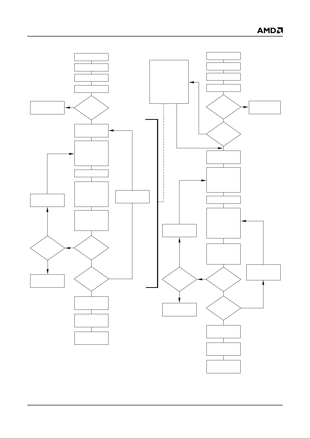
Sector Protection/Unprotection
The hardware sector protection feature disables both
program and erase operations in any sect or. The hardware sector unprotection feature re-enables both program and erase operations in previously protected
sectors. Sector protection/unprotecti on can be implemented via two methods.
The primary method requires V
ID
on the RESET# pin
only, and can be implemented either in-system or via
programming equipment. Figure 1 shows the algorithms and Figure 23 shows the timing diagram. This
method uses standard m icroprocessor bus cycle timing. For sector unprotect, all unprotected sectors must
first be protected prior to the first sector unpro tect write
cycle.
The alternate method intended on ly for programming
equipment requires V
ID
on address pin A9 and OE#.
This method is compatible with programmer routines
written for earlier 3.0 v olt-only AMD flash de vices. Publication number 21622 contains further details. Contact
an AMD representative to request the document containing further details.
The device is shipped with all sectors unprotected.
AMD offers the option of programming and protecting
sectors at its factory prior to shipping the device
through AMD’s ExpressFlash™ Servic e. Contact an
AMD representative for details.
It is possible to determine whether a sector is protected
or unprotected. See “Autoselect Mode” for details.
Temporary Sector Unprotect
This feature allows temporary unprotection of previously protected sectors to change data in-system. The
Sector Unprotect mode is activated by setting the RESET# pin to V
ID
. During this mode, formerly protected
sectors can be programmed or erased b y selecting the
sector addresses. Once V
ID
is removed from the RESET# pin, all the previously protected sectors are
protected again. Figure 2 shows the algorithm, and
Figure 22 shows the timing diagrams, for this feature.
Description Mode CE # OE# WE#
A18
to
A12
A11
to
A10 A9
A8
to
A7 A6
A5
to
A2 A1 A0
DQ8
to
DQ15
DQ7
to
DQ0
Manufacturer ID: AMD L L H X X V
ID
XLXLL X 01h
Device ID:
Am29SL800B
(Top Boot Block)
Word L L H
XXVIDXLXLH
22h EAh
Byte L L H X EAh
Device ID:
Am29SL800B
(Bottom Boot
Block)
Word L L H
XXV
ID
XLXLH
22h 6Bh
Byte L L H X 6Bh
Sector Protection V erification L L H SA X V
ID
XLXHL
X
01h
(protected)
X
00h
(unprotected)
Am29SL800B 13
ADVANCE INFORMATION
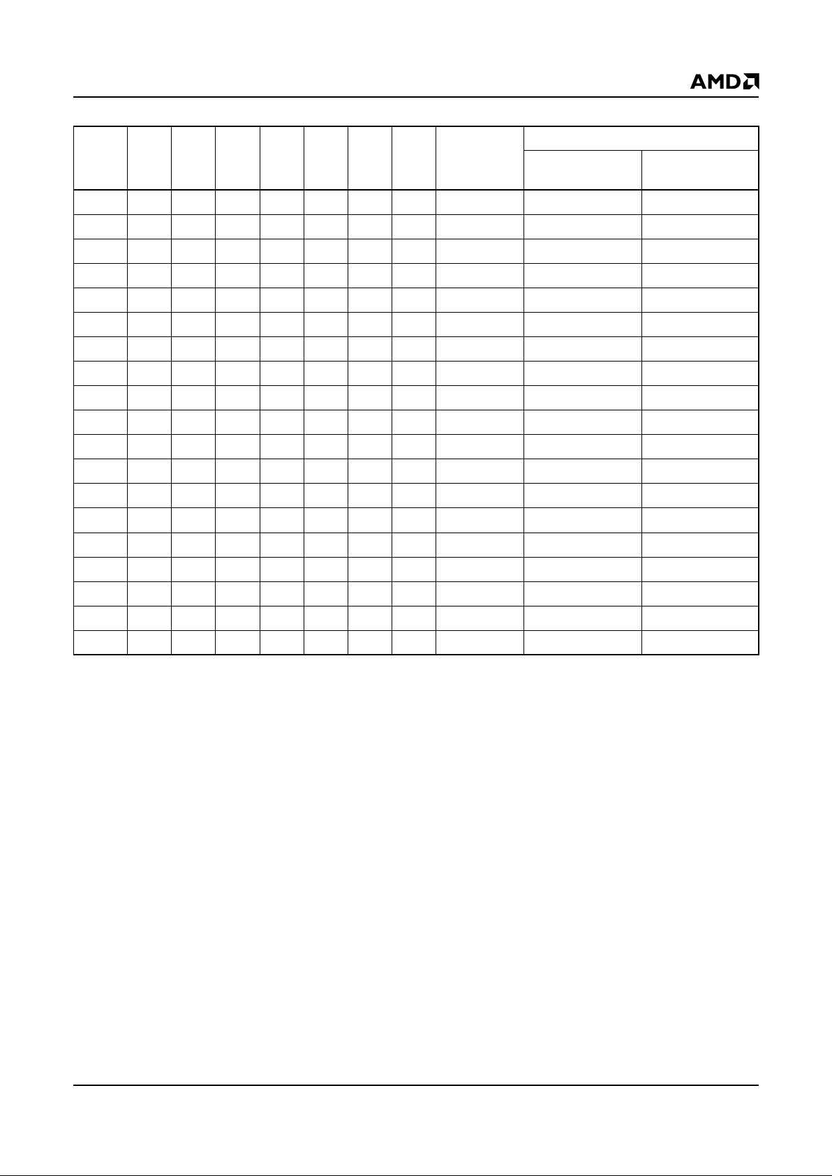
Figure 1. In-System Sector Protect/Unprotect Algorithms
Sector Protect:
Write 60h to sector
address with
A6 = 0, A1 = 1,
A0 = 0
Set up sector
address
Wait 150 µs
Verify Sector
Protect: Write 40h
to sector address
with A6 = 0,
A1 = 1, A0 = 0
Read from
sector address
with A6 = 0,
A1 = 1, A0 = 0
START
PLSCNT = 1
RESET# = V
ID
Wait 1 µs
First Write
Cycle = 60h?
Data = 01h?
Remove V
ID
from RESET#
Write reset
command
Sector Protect
complete
Yes
Yes
No
PLSCNT
= 25?
Yes
Device failed
Increment
PLSCNT
Temporary Sector
Unprotect Mode
No
Sector Unprotect:
Write 60h to sector
address with
A6 = 1, A1 = 1,
A0 = 0
Set up first sector
address
Wait 15 ms
Verify Sector
Unprotect: Write
40h to sector
address with
A6 = 1, A1 = 1,
A0 = 0
Read from
sector address
with A6 = 1,
A1 = 1, A0 = 0
START
PLSCNT = 1
RESET# = V
ID
Wait 1 µs
Data = 00h?
Last sector
verified?
Remove V
ID
from RESET#
Write reset
command
Sector Unprotect
complete
Yes
No
PLSCNT
= 1000?
Yes
Device failed
Increment
PLSCNT
Temporary Sector
Unprotect Mode
No
All sectors
protected?
Yes
Protect all sectors:
The indicated portion
of the sector protect
algorithm must be
performed for all
unprotected sectors
prior to issuing the
first sector
unprotect address
Set up
next sector
address
No
Yes
No
Yes
No
No
Yes
No
Sector Protect
Algorithm
Sector Unprotect
Algorithm
First Write
Cycle = 60h?
Protect another
sector?
Reset
PLSCNT = 1
21545A-5
 Loading...