


AM29F040B-90PIB
AMD Advanced Micro Devices AM29F040B-90PIB, AM29F040B-90PI, AM29F040B-90PEB, AM29F040B-90PCB, AM29F040B-90PC Datasheet
...
PRELIMINARY
Am29F040B
4 Megabit (512 K x 8-Bit)
CMOS 5.0 Volt-only, Uniform Sector Flash Memory
Distinctive Characteristics
■ 5.0 V ± 10% for read and write operations
— Minimizes system level power requirements
■ Manufactured on 0.35 µm process technology
— Compatible with 0.5 µm Am29F040 device
■ High performance
— Access times as fast as 55 ns
■ Low power consumption
— 20 mA typical active read current
— 30 mA typical program/erase current
— 1 µA typical standby current (standard access
time to active mode)
■ Flexible sector architecture
— 8 uniform sectors of 64 Kbytes each
— Any combination of sectors can be erased
— Supports full chip erase
— Sector protection:
A hardware method of locking sector s to prev ent
any program or erase operat ions within that
sector
■ Embedded Algorithms
— Embedded Erase algorithm automatically
preprograms and erases the entire chip or any
combination of designated sectors
— Embedded Program algorithm automatically
writes and verifies bytes at specified addresses
■ Minimum 1,000,000 progr am/erase cycles per
sector guaranteed
■ Package options
— 32-pin PLCC, TSOP, or PDIP
■ Compatible with JEDEC standards
— Pinout and software c ompatible with
single-power-supply Flash standard
— Superior inadvertent write protection
■ Data# Polling and toggle bits
— Provides a software method of detecting
program or erase cycle completion
■ Erase Suspend/Erase Resume
— Suspends a sector erase oper ation to read da ta
from, or program data to, a non-erasing sector,
then resumes the erase operation
Publication# 21445 Rev: B Amendment/+2
Issue Date: April 1998

PRELIMINARY
GENERAL DESCRIPTION
The Am29F040B is a 4 Mbit, 5.0 volt-only Flash memory organized as 524,288 Kbytes of 8 bits each. The
512 Kbytes of data are div ided into eight sectors of 64
Kbytes each for flexible erase capability. The 8 bits of
data appear on DQ0–DQ7. The Am29F040B is offered
in 32-pin PLCC, TSOP, and PDIP packages. This device is designed to be programmed in-system with the
standard system 5.0 volt V
not required for write or erase operations. The device
can also be programmed i n standard EPROM programmers.
This device is manufactured using AMD’s 0.35 µm
process technology, and off ers all the f eatures and benefits of the Am29F040, which was manufactured using
0.5 µm process technology. In addtion, the
Am29F040B has a second toggle bit, DQ2, and also
offers the ability to program in the Erase Suspend
mode.
The standard Am29F040B o ffers access times of 55,
70, 90, 120, and 150 ns, allowing high-s peed microprocessors to operate without w ait states . To eliminate b us
contention the device has separate chip enable (CE#),
write enable (WE#) and output enable (OE#) controls.
The device requires only a single 5. 0 v o lt po wer sup-
ply for both read and wr ite functions. Internally generated and regulated voltages are provided for the
program and erase operations.
The device is entirely command set compatible with the
JEDEC single-power-supply Flash standard. Commands are written to the command register using standard microproc essor write timing s. Register contents
serve as input to an internal sta te-machine that co ntrols the erase and programming circuit ry. Write cycles
also internally latch addresses and data needed f or the
programming and erase operations. Reading data out
of the device is similar to reading from other Flash or
EPROM devices.
Device programming occurs by executing the program
command sequence. This initiates the Embedded
Program algorithm—an internal algorithm that auto-
supply. A 12.0 volt VPP is
CC
matically times the program pulse widths an d verifies
proper cell margin.
Device erasure occurs by executing the erase command sequenc e. This initiates the Embedded Erase
algorithm—an in ternal algorithm that auto matically
preprograms the arra y (if it is not already progr ammed)
before e xecuting the er ase operation. During erase, the
device automatically times the erase pulse widths and
verifies proper cell margin.
The host system can detect whether a program or
erase operation is complete by reading the DQ7 (Data#
Polling) and DQ6 (toggle) status bits. After a program
or erase cycle has been completed, the de vice is ready
to read array data or accept another command.
The sector erase ar chitecture allo ws memo ry secto rs
to be erased and reprogrammed without affecting the
data contents of other sectors. The device is fully
erased when shipped from the factory.
Hardware data protection measures include a low
detector that automatically in hibits write opera-
V
CC
tions during power transitions. The hardware sector
protection feature disables both program and erase
operations in any combination of the sectors of memory . This can be achie v ed via prog ramming equipment.
The Erase Suspend feature enables the user to put
erase on hold for any period of time to read data from,
or program data to, any s ector that is not selected for
erasure. True background erase can thus be achie ved.
The system can place the device into the standby
mode. Power consum ption is greatly reduced in
this mode.
AMD’s Flash technology combines years of Flash
memory manufacturing exper ience to produce the
highest levels of quality, reliability and cost effectiveness. The device electrically erases all bi t s w i th i n a
sector simultaneously via Fowler-Nordheim t unneling. The data is programmed using hot electron injection.
2 Am29F040B
PRELIMINARY
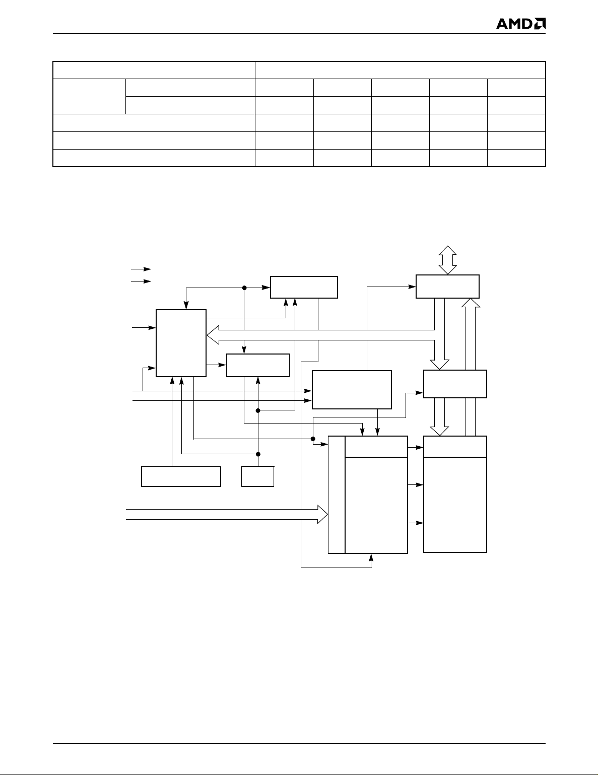
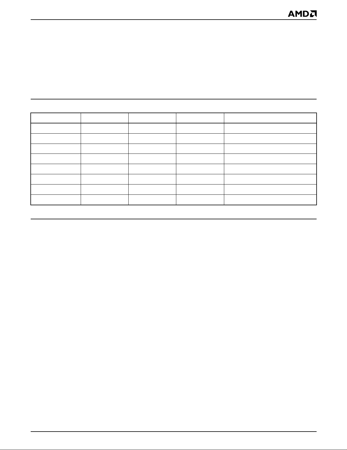
PRODUCT SELECTOR GUIDE
Family Part Number Am29F040B
= 5.0 V ± 5% -55
V
Speed Option
Max access time, ns (t
CC
= 5.0 V ± 10% -70 -90 -120 -150
V
CC
) 55 70 90 120 150
ACC
Max CE# access time, ns (tCE) 55 70 90 120 150
Max OE# access time, ns (tOE) 2530355055
Note: See the “AC Characteristics” section for more information.
BLOCK DIAGRAM
DQ0–DQ7
V
CC
V
SS
Erase Voltage
Generator
Input/Output
Buffers
WE#
CE#
OE#
A0–A18
State
Control
Command
Register
V
Detector
CC
PGM Voltage
Generator
Timer
Chip Enable
Output Enable
STB
Logic
Y-Decoder
Address Latch
STB
Data Latch
Y-Gating
Cell MatrixX-Decoder
21445B-1
Am29F040B 3
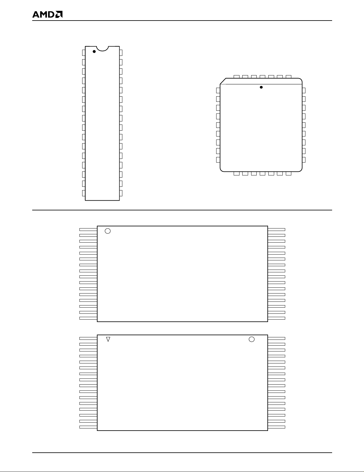
CONNECTION DIAGRAMS
PRELIMINARY
A18
A16
A15
A12
DQ0
DQ1
DQ2
V
A11
A9
A8
A13
A14
A17
WE#
V
CC
A18
A16
A15
A12
A7
A6
A5
A4
A7
A6
A5
A4
A3
A2
A1
A0
SS
1
2
3
4
5
6
7
8
9
10
11
12
13
14
15
16
PDIP
1
2
3
4
5
6
7
8
9
10
11
12
13
14
15
16
32
31
30
29
28
27
26
25
24
23
22
21
20
19
18
17
V
CC
WE#
A17
A14
A13
A8
A9
A11
OE#
A10
CE#
DQ7
DQ6
DQ5
DQ4
DQ3
21445B-2
32-Pin Standard TSOP
A7
A6
A5
A4
A3
A2
A1
A0
DQ0
5
6
7
8
9
10
11
12
13
A12
DQ1
A15
A16
A18
1313023432
PLCC
17 18 19 20161514
SS
V
DQ2
DQ3
32
31
30
29
28
27
26
25
24
23
22
21
20
19
18
17
VCCWE#
DQ4
DQ5
OE#
A10
CE#
DQ7
DQ6
DQ5
DQ4
DQ3
V
DQ2
DQ1
DQ0
A0
A1
A2
A3
A17
29
28
27
26
25
24
23
22
21
DQ6
SS
A14
A13
A8
A9
A11
OE#
A10
CE#
DQ7
21445B-3
OE#
A10
CE#
DQ7
DQ6
DQ5
DQ4
DQ3
V
SS
DQ2
DQ1
DQ0
A0
A1
A2
A3
1
2
3
4
5
6
7
8
9
10
11
12
13
14
15
16
32-Pin Reverse TSOP
4 Am29F040B
32
31
30
29
28
27
26
25
24
23
22
21
20
19
18
17
A11
A9
A8
A13
A14
A17
WE#
V
CC
A18
A16
A15
A12
A7
A6
A5
A4
21445B-4
PRELIMINARY
PIN CONFIGURATION
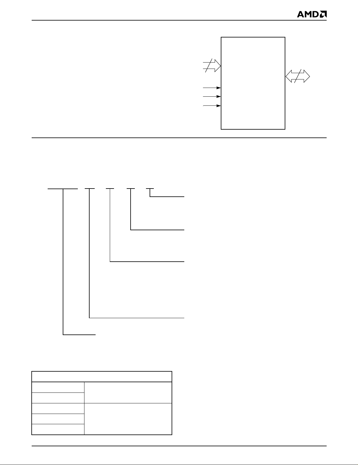
LOGIC SYMBOL
A0–A18 = Address Inputs
DQ0–DQ7 = Data Input/Output
CE# = Chip Enable
WE# = Write Enable
19
A0–A18
8
DQ0–DQ7
OE# = Output Enable
V
SS
= Device Ground
VCC = +5.0 V single power supply
(see Product Selector Guide for
CE#
OE#
WE#
device speed ratings and voltage
supply tolerances)
21445B-5
ORDERING INFORMATION
Standard Pr od ucts
AMD standard products are available in several packages and operating ranges. The order number (Valid Combination) is formed
by a combination of the following:
Am29F040B -55 E C
B
OPTIONAL PROCESSING
Blank = Standard Processing
B = Burn-in
(Contact an AMD representative for more information)
Am29F040B-55
Am29F040B-70
Am29F040B-90
Am29F040B-120
Am29F040B-150
DEVICE NUMBER/DES CR IPT IO N
Am29F040B
4 Megabit (512 K x 8-Bit) CMOS 5.0 Volt-only Sector Erase Flash Memory
5.0 V Read, Program, and Erase
Valid Combinations
JC, JI, JE, EC, EI, EE, FC, FI, FE
PC, PI, PE,
JC, JI, JE,
EC, EI, EE,
FC, FI, FE
TEMPERATURE RANGE
C = Commercial (0
I=Industrial (–40
E = Extended (–55
PACKAGE TYPE
P = 32-Pin Plastic DIP (PD 032)
J = 32-Pin Rectangular Plastic Leaded Chip
Carrier (PL 032)
E = 32-Pin Thin Small Outline Package (TSOP)
Standard Pinout (TS 032)
F = 32-Pin Thin Small Outline Package (TSOP)
Reverse Pinout (TSR032)
SPEED OPTION
See Product Selector Guide and Valid Combinations
Valid Combinations list configurations planned to be supported in volume for this device. Consult the local AMD sales
office to confirm availability of specific valid combinations and
to check on newly released combinations.
°C to +70°C)
°C to +85°C)
°C to +125°C)
Valid Combinations
Am29F040B 5
PRELIMINARY
DEVICE BUS OPERATIONS
This section describes the requirements and use of the
device bus operations, which are initiated through the
internal c ommand register. The command register itself does not occupy any addressable memory location. The register is composed of l atches that store the
commands, along with the address and data informa-
tion needed to execute the command. The contents of
the register serve as inputs to the internal state machine. The state machine outputs dictate the function of
the device. The appropriate device bus operations
table lists the inputs and control le vels requ ired, and the
resulting output. The following subsections describe
each of these operations in further detail.
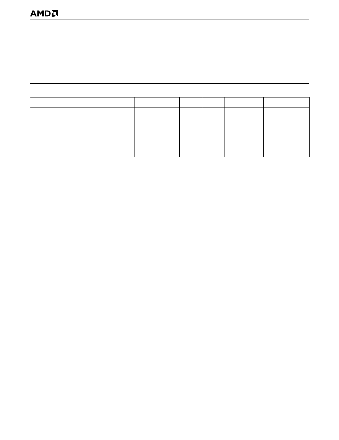
Table 1. Am29F040B Device Bus Operations
Operation CE# OE# WE# A0–A20 DQ0–DQ7
Read L L H A
Write L H L A
CMOS Standby VCC ± 0.5 V X X X High-Z
TTL Standby H X X X High-Z
Output Disable L H H X High-Z
Legend:
L = Logic Low = V
Note: See the section on Sector Protection for more information.
, H = Logic High = VIH, VID = 12.0 ± 0.5 V, X = Don’t Care, DIN = Data In, D
IL
IN
IN
= Data Out, AIN = Address In
OUT
D
OUT
D
IN
Requirements for Reading Array Data
To read array data from the outputs, the system must
drive the CE# and OE# pins to V
. CE# is the power
IL
control and selects the device. OE# is the output control
and gates array data to the output pins. WE# should remain at V
.
IH
The internal state machin e is set for reading array
data upon device power-up, or after a hardware reset.
This ensures that no spurious alteration of the memory content occurs during the power transition. No
command is necessar y in this mode to obtain array
data. Standard microprocessor read cycles that assert valid addresses on the device address inputs
produce valid data on the device data outputs. The
device remains enable d for read access until the
command register contents are altered.
See “Reading Array Data” for more information. Refer
to the AC Read Operations table for timing specifications and to the Read Operations Timings diagram for
the timing waveforms. I
in the DC Characteristics
CC1
table represents the active current specification for
reading array data.
Writing Commands/Command Sequences
To write a command or command sequence (which includes programming data to the device and erasing
sectors of memory), the system must drive WE# and
CE# to V
An erase operation can erase one sect or, multiple sectors, or the entire de vice. The Sector Address Tables in-
, and OE# to VIH.
IL
dicate the address space that each sector occupies. A
“sector address” consists of the address bits required
to uniquely select a sector. See the “Command Definitions” section for details on erasing a sector or the entire chip, or suspending/resuming the erase operation.
After the system writes the autoselect command sequence, the device enters the autoselect mode. The
system can then read autoselect codes from the internal register (which is separate from the memory array)
on DQ7–DQ0. Standard read cycle timings apply in this
mode. Refer to the “Autoselect Mode” and “Autoselect
Command Sequence” sections for more information.
in the DC Characteristics table represents the ac-
I
CC2
tive current specification for the write mode. The “AC
Characteristics” section contains timing specification
tables and timing diagrams for write operations.
Program and Erase Operation Status
During an erase or program operation, the system ma y
check the status of the operation by reading the status
bits on DQ7–DQ0. Standard read cycle timings and I
CC
read specifica tions apply. Refer to “Write Operation
Status” for more infor mation, and to each AC Characteristics section for timing diagrams.
Standby Mode
When the system is not reading or writing to the device ,
it can place the device in the standby mode. In this
mode, current consumption is gr eatly reduced, and the
outputs are placed in the high impedance state, independent of the OE# input.
6 Am29F040B
PRELIMINARY
The device enters the CMOS standby mode when the
CE# pin is held at V
restricted voltage rang e than V
the TTL standby mode when CE# is held at V
device requires the standard ac cess time (t
± 0.5 V. (Note that this is a more
CC
.) The device enters
IH
) before it
CE
IH
. The
is ready to read data.
If the device is deselected during erasure or program -
in the DC Characteristics tables represents the
I
CC3
standby current specification.
Output Disable Mode
When the OE# input is at VIH, output from the device is
disabled. The output pins are placed in t he high impedance state.
ming, the device draws active current until the
operation is completed.
Table 2. Sector Addresses Table
Sector A18 A17 A16 Address Range
SA0 0 0 0 00000h–0FFFFh
SA1 0 0 1 10000h–1FFFFh
SA2 0 1 0 20000h–2FFFFh
SA3 0 1 1 30000h–3FFFFh
SA4 1 0 0 40000h–4FFFFh
SA5 1 0 1 50000h–5FFFFh
SA6 1 1 0 60000h–6FFFFh
SA7 1 1 1 70000h–7FFFFh
Note: All sectors are 64 Kbytes in size.
Autoselect Mode
The autoselect mode provides manufacturer and device identification, and sector protection verification,
through identifier codes output on DQ7–DQ0. This
mode is primarily intended for progr amming equipment
to automatically match a device to be progr ammed with
its correspondi ng programming al gorithm. However,
the autoselect codes can also be accessed in-system
through the command register.
When using programming equipment, the autoselect
mode requires V
A9. Address pins A6, A1, and A0 must be as shown in
Autoselect Codes (High Voltage Method) table. I n addition, when verifying sector protection, the sector ad-
(11.5 V to 12.5 V) on address pin
ID
dress must appear on the appropriate highest order
address bits. Refer to the corresponding Sector Address Tables. The Comm and Definitions table shows
the remaining address bits that are don’t c are. When all
necessary bits have been set as required, the programming equipment may then read the corresponding
identifier code on DQ7–DQ0.
To access the autoselect codes in-system, the host
system can issue the autoselect command via the
command register, as shown in the C ommand Definitions table. This method does not require V
. See
ID
“Command Definitions” for details on using the autoselect mode.
Am29F040B 7

PRELIMINARY
Table 3. Am29F040B Autoselect Codes (High Voltage Method)
Description A18–A16 A15–A10 A9 A8–A7 A6 A5–A2 A1 A0
Identifier Code on
DQ7-DQ0
Manufacturer ID: AMD X X V
Device ID: Am29F040B X X V
Sector Protection
Ve r ific atio n
Sector
Address
XV
ID
ID
ID
Sector Protection/Unprotection
The hardware sector protection feature disables both
program and erase operations in any sector. The
hardware sector unprotection feature re-enables both
program and erase operations in previously protected sectors.
Sector protection/unprotection must be implemented
using programming equipment. The procedure requires a high voltage (V
) on address pin A9 and the
ID
control pins. Details on this method are provided in a
supplement, publication number 19957. Contact an
AMD representative to obtain a cop y of the appropriate
document.
The device is shipped with all sectors unprotected.
AMD offers the option of programming and protecting
sectors at its factory prior to shipping the device
through AMD’s ExpressFlash™ Servic e. Contact an
AMD representative for details.
It is possible to determine whether a sector is protected
or unprotected. See “Autoselect Mode” for details.
Hardware Data Protection
The command sequence requirement of unlock cycles
for programming or erasing provides data protection
against inadvertent writes (refer to the Command Definitions table). In addition, the following hardware data
protection measures pre vent accidental eras ure or pro-
XVILXVILV
XVILXVILV
XVILXVIHV
IL
IH
IL
01h
A4h
01h (protected)
00h (unprotected)
gramming, which might otherwise be caused by spurious system level signals during V
power-up and
CC
power-down transitions, or from system noise.
Low V
When V
Write Inhibit
CC
is less than V
CC
, the device does not ac-
LKO
cept any write cycles. This protects data during V
power-up and power-down. The command register and
all internal program/erase circuits are disabled, and the
device resets. Subsequent writes are ignored until V
is greater than V
. The system must provide the
LKO
proper signals to the control pins to prevent unintentional writes when V
is greater than V
CC
LKO
.
Write Pulse “Glitch” Protection
Noise pulses of less than 5 ns (typical) on OE#, CE# or
WE# do not initiate a write cycle.
Logical Inhibit
Write cycles are inhibited by holding any one of OE# =
, CE# = VIH or WE# = VIH. To initiate a write cycle,
V
IL
CE# and WE# must be a logical zero while OE# is a
logical one.
Power-Up Write Inhibit
If WE# = CE# = V
and OE# = VIH during power up , the
IL
device does not accept commands on the rising edge
of WE#. The internal state mac hine is automatically
reset to reading array data on power-up.
CC
CC
COMMAND DEFINITIONS
Writing specific addre ss and data commands or sequences into the command register initiates device operations. The Command Definitions table defines the
valid register command sequences. Writing incorrect
address and data values or writing them in the im-
proper sequence resets the device to reading array
data.
All addresses are latched on the falling edge of WE# or
CE#, whichever happens later. All data is latched on
the rising edge of WE# or CE#, whichever happens
first. Refer to the appropriate timing diagrams in the
“AC Characteristics” section.
8 Am29F040B
Reading Array Data
The device is automatically set to reading array data
after device power-up. No commands are required to
retrieve data. The device is also ready to read array
data after completing an Embedded Program or Embedded Erase algorithm.
After the device accepts an Era se Suspend command,
the device enters the Erase Suspend mode. The system can read array data using the standard read timings, except that if it reads at an address within erasesuspended sectors, the device outputs status data.
After completing a progr amming operation in the Erase
Suspend mode, the system may once again read array

PRELIMINARY
data with the same ex ception. See “Erase Suspend/
Erase Resume Commands” for more information on
this mode.
must
The system
able the dev ice f or reading arra y data if DQ5 goes high,
or while in the autoselect mode. See the “Reset Command” section, next.
See also “Requirements for Reading Arr a y Data” in the
“Device Bus Operations” section for more information.
The Read Operations table provides the read parameters, and Read Operation Tim ings diagram shows the
timing diagram.
issue the reset command to re-en-
Reset Command
Writing the reset command to the devi ce resets the device to reading array data. Address bits are don’t care
for this command.
The reset command may be written between the sequence cycles in an erase command sequence before
erasing begins. This resets the device to reading array
data. Once erasure begins, however, the device ignores reset commands until the operation is complete.
The reset command may be written between the sequence cycles in a program command sequence before programming begins. This resets the device to
reading array data (also applies to programming in
Erase Suspend mode). Once programming begins,
however, the device ignores reset commands until the
operation is complete.
The reset command may be written between the sequence cycles in an autoselect command sequence.
Once in the autoselect mode, t he reset c ommand
be written to return to reading array data (als o applies
to autoselect during Erase Suspend).
If DQ5 goes high during a program or erase operation,
writing the reset command returns the device to reading array data (also applies during Erase Suspend).
must
Autoselect Command Sequence
The autoselect command sequence allows the host
system to access the manufacturer and devices codes ,
and determine whether or not a sector is protected.
The Command Definitions table shows the address
and data requirements. This method is an alternative to
that shown in the Autoselect Codes (High Voltage
Method) table, which is in tended for PROM programmers and requires VID on address bit A9.
The autoselect command sequence is initiated by
writing two unlock cycles, followed by the autoselect
command. The device then en ters the autoselect
mode, and the system may read at any address any
number of times, without initiating another command
sequence.
A read cycle at address XX00h or retrieves the manufacturer code. A read cycle at address XX 01h returns
the device code. A read cycle containing a sector address (SA) and the address 02h in returns 01h if that
sector is protect ed, o r 0 0h if it i s unp rotec te d. Refer to
the Sector Address tables for valid sector addresses.
The system must write the reset command to exit the
autoselect mode and return to reading array data.
Byte Program Command Sequence
Programming is a four-bus-cycle operation. The program command sequence is initiated by writing two unlock write cycles, followed by the program set-up
command. The program address and data are wr itten
next, which in turn initiate the Embedded Program al-
not
gorithm. The system is
controls or timings. The device automatically provides
internally generated program pulses and v erify the programmed cell margin. The Command Definitions take
shows the address and data requirements for the byte
program command sequence.
When the Embedded Program algorithm is complete,
the device then returns to reading array data and addresses are no longer latched. The system can determine the status of the prog ram oper ation b y using DQ7
or DQ6. See “Wr ite Operation Status” for information
on these status bits.
Any commands written to the device dur ing the Embedded Program Algorithm are ignored.
Programming is allowed in any sequence an d across
sector boundaries. A bit cannot be programmed
from a “0” back to a “1”. Attempting to do so may halt
the operation and set DQ5 to “1”, or cause the Data#
Polling algorithm to indic ate the operation was successful. However, a succeeding read will show that the
data is still “0”. Only erase operations can convert a “0”
to a “1”.
required to provide further
Am29F040B 9
 Loading...