


AM29LV102BT-90ECB
AMD Advanced Micro Devices AM29LV102BT-90ECB, AM29LV102BT-90EC, AM29LV102BT-70JIB, AM29LV102BT-70JI, AM29LV102BT-70JEB Datasheet
...
ADVANCE INFORMATION
Am29LV102B
2 Megabit (256 K x 8-Bit)
CMOS 3.0 Volt-only, Boot Sector 32-Pin Flash Memory
DISTINCTIVE CHARACTERISTICS
■ Single power supply operation
— Full voltage range: 2.7 to 3. 6 volt read and write
operations for battery-powered applications
— Regulated voltage r ange: 3.0 to 3.6 v olt read and
write operations and for compatibility with high
performance 3.3 volt microprocessors
■ Manufactured on 0.35 µm process technology
■ High performance
— Full voltage range: ac cess times as f ast as 70 ns
— Regulated voltage range: access times as fast
as 55 ns
■ Ultra low power consumption
— Automatic sleep mode: 1 µA (typical values at
5MHz)
— Standby mode: 1 µA
— Read mode: 7 mA
— Program/erase mode: 15 mA
■ Flexible sector architecture
— One 16 Kbyte, two 8 Kbyte, one 32 Kbyte, and
three 64 Kbyte sectors
— Any combination of sectors can be erased;
supports full chip erase
— Sector Protection features:
Hardware method of loc king a sector to prevent
any program or erase operat ions within that
sector
Sectors can be locked via programming
equipment
■ Unlock Bypass Program Command
— Reduces overall programming time when
issuing multiple program command sequences
■ Embedded Algorithms
— Embedded Erase algorithms automatically
preprogram and erase the entire chip or any
combination of designated sectors
— Embedded Program algorithms automatically
writes and verifies data at specified addresses
■ Minimum 1,000,000 write/erase cycles
guaranteed
■ Package option
— 32-pin PLCC
— 32-pin TSOP
■ Compatibility with JEDEC standards
— Pinout and software compatible with single-
power supply Flash
— Superior inadvertent write protection
■ Data# Polling and toggle bits
— Provides a software method of detecting
program or erase cycle completion
■ Erase Suspend/Resume
— Supports reading data from or programming
data to a sector not being erased
This document contains information on a product under development at Advanced Micro Devices. The information
is intended to help you ev aluate this product. AMD reserves the right to change or dis continue work on thi s proposed
product without notice. 2/9/98
Refer to AMD’s Website (www.amd.com) for the latest information.
Publication# 21259 Rev: A Amendment/0
Issue Date: January 1998

ADVANCE INFORMATION
GENERAL DESCRIPTION
The Am29LV102B is a single power s upply, 2 Mbit, 3.0
Volt-only Flash memor y device organized as 262,144
bytes. The data appears on DQ0-DQ7. The device is
available in 32-pin PLCC and 32-pin TSOP packages.
All read, erase, and program operations are accomplished using only a single power supply. The device
can also be programmed i n standard EPROM programmers.
The device offers access times of 55, 70, 90, and 120
ns allowing high speed microprocessors to operate
without wait states. To eliminate bus contention, the
device has separate control pins—chip enable (CE#),
write enable (WE#), and output enable (OE#)—to
control normal read and write operations.
The device requires only a single power supply (2.7
V–3.6V) for both read and write functions. Internally
generated and regulated voltages are provided for the
program and erase operations.
The device is entirely command set compatible with the
JEDEC single-power-supply Flash standard. Commands are written to the command regis ter using
standard micropr ocessor wri te timings. Register co ntents serve as input to an internal state-machine that
controls the erase and programming circuitry. Write
cycles also internally latch addresses and data needed
for the programming and erase operations. Reading
data out of the device is similar to reading from other
Flash or EPROM devices.
Device programming occurs by executing the program
command sequence. This initiates the Embedded
Program algorithm—an internal algorithm that automatically times the program pulse widths and verifies
proper cell margin. The Unlock Bypass mode facilitates faster programming times by requir ing only two
write cycles to program data instead of four.
Device erasure occurs by executing the erase command sequence. This initiates the Embedded Erase
algorithm—an in ternal algorithm that autom atically
preprograms the array (if it is not already prog rammed)
before e xecuting the er ase operation. During erase, the
device automatically times the erase pulse widths and
verifies proper cell margin.
The host system can detect whether a program or
erase operation is complete by reading the DQ7 (Data#
Polling) and DQ6 (toggle) status bits. After a program
or erase cycle has been completed, the de vice is ready
to read array data or accept another command.
The sector erase ar chitecture allo ws memo ry secto rs
to be erased and reprogrammed without affecting the
data contents of other sectors. The device is fully
erased when shipped from the factory.
Hardware data protection measures include a low
detector that automatically in hibits write opera-
V
CC
tions during power transitions. The hardware sector
protection feature disables both program and erase
operations in any combination of the sectors of memory. This is achieved via programming equipment.
The Erase Suspend feature enables the user to put
erase on hold for any period of time to read data from,
or program data to, any sector that is not selected for
erasure. True background erase can thus be achiev ed.
The device off ers two power-sa ving f eatures. When addresses have been stable for a specified amount of
time, the device enters the automatic sleep m ode.
The system can also place the de vice into the standby
mode. Power consumption is greatly reduced in both
these modes.
AMD’s Flash technology combines years of Flash
memory manufacturing experience to produce the
highest levels of quality, reliability and cost effectiveness. The device electrically erases all bi t s w i th i n a
sector simultaneously via Fowler-Nordheim tunneling. The data is programmed using hot electron
injection.
2 Am29LV102B 2/9/98
ADVANCE INFORMATION
PRODUCT SELECTOR GUIDE
Family Part Number Am29LV102B
Speed Options
Max access time, ns (t
Max CE# access time, ns (tCE) 55 70 90 120
Max OE# access time, ns (tOE) 30 30 30 35
Regulated Voltage Range: VCC =3.0–3.6 V -55R
Full Voltage Range: VCC = 2.7–3.6 V -70 -90 -120
) 55 70 90 120
ACC
Note: See “AC Characteristics” for full specifications.
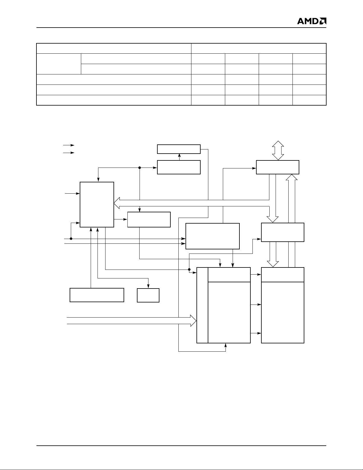
BLOCK DIAGRAM
DQ0
DQ7
–
V
CC
V
SS
WE#
CE#
OE#
State
Control
Command
Register
PGM Voltage
Generator
Sector Switches
Erase Voltage
Generator
Chip Enable
Output Enable
Logic
STB
Input/Output
Buffers
Data
Latch
A0–A17
VCC Detector
Timer
STB
Address Latch
Y-Decoder
X-Decoder
Y-Gating
Cell Matrix
2/9/98 Am29LV102B 3
 Loading...