


AMD Advanced Micro Devices AM29F040-120EC, AM29F040-120PI, AM29F040-120PE, AM29F040-120PCB, AM29F040-120PC Datasheet
...FINAL
Am29F040
4 Megabit (524,288 x 8-Bit) CMOS 5.0 Volt-only, Sector Erase Flash Memory
DISTINCTIVE CHARACTERISTICS
■5.0 V ± 10% for read and write operations
—Minimizes system level power requirements
■Compatible with JEDEC-standards
—Pinout and software compatible with single- power-supply Flash
—Superior inadvertent write protection
■Package options
—32-pin PLCC
—32-pin TSOP
—32-pin PDIP
■Minimum 100,000 write/erase cycles guaranteed
■High performance
—55 ns maximum access time
■Sector erase architecture
—Uniform sectors of 64 Kbytes each
—Any combination of sectors can be erased.
Also supports full chip erase.
■ Sector protection
■Embedded Erase Algorithms
—Automatically preprograms and erases the chip or any combination of sectors
■Embedded Program Algorithms
—Automatically programs and verifies data at specified address
■Data Polling and Toggle Bit feature for detection of program or erase cycle completion
■Erase suspend/resume
—Supports reading data from a sector not being erased
■Low power consumption
—20 mA typical active read current
—30 mA typical program/erase current
■Enhanced power management for standby mode
—<1 A typical standby current
—Standard access time from standby mode
—Hardware method that disables any combination of sectors from write or erase operations
GENERAL DESCRIPTION
The Am29F040 is a 4 Mbit, 5.0 Volt-only Flash memory organized as 512 Kbytes of 8 bits each. The Am29F040 is offered in a 32-pin package. This device is designed to be programmed in-system with the standard system 5.0 V VCC supply. A 12.0 V VPP is not required for write or erase operations. The device can also be reprogrammed in standard EPROM programmers.
The standard Am29F040 offers access times between 55 ns and 150 ns, allowing operation of high-speed microprocessors without wait states. To eliminate bus contention the device has separate chip enable (CE), write enable (WE) and output enable (OE) controls.
The Am29F040 is entirely command set compatible with the JEDEC single-power-supply Flash standard. Commands are written to the command register using standard microprocessor write timings. Register contents serve as input to an internal state machine
which controls the erase and programming circuitry. Write cycles also internally latch addresses and data needed for the programming and erase operations. Reading data out of the device is similar to reading from 12.0 Volt Flash or EPROM devices.
The Am29F040 is programmed by executing the program command sequence. This will invoke the Embedded Program Algorithm which is an internal algorithm that automatically times the program pulse widths and verifies proper cell margin. Typically, each sector can be programmed and verified in less than one second. Erase is accomplished by executing the erase command sequence. This will invoke the Embedded Erase Algorithm which is an internal algorithm that automatically preprograms the array if it is not already programmed before executing the erase operation. During erase, the device automatically times the erase pulse widths and verifies proper cell margin.
Publication# 17113 Rev: E Amendment/0
Issue Date: November 1996
Any individual sector is typically erased and verified in 1.0 seconds (if already completely preprogrammed).
This device also features a sector erase architecture. The sector mode allows for 64K byte blocks of memory to be erased and reprogrammed without affecting other blocks. The Am29F040 is erased when shipped from the factory.
The device features single 5.0 V power supply operation for both read and write functions. Internally generated and regulated voltages are provided for the program and erase operations. A low VCC detector automatically inhibits write operations on the loss of power.The end of program or erase is detected by Data Polling of DQ7 or by the Toggle Bit feature on DQ6. Once the end of a program or erase cycle has been completed, the device internally resets to the read mode.
AMD’s Flash technology combines years of EPROM and E2PROM experience to produce the highest levels of quality, reliability and cost effectiveness. The Am29F040 memory electrically erases the entire chip or all bits within a sector simultaneously via FowlerNordheim tunneling. The bytes are programmed one byte at a time using the EPROM programming mechanism of hot electron injection.
Flexible Sector-Erase Architecture
■Eight 64 Kbyte sectors
■Individual-sector, multiple-sector, or bulk-erase capability
■Individual or multiple-sector protection is user definable
7FFFFh
6FFFFh
5FFFFh
64 Kbytes per Sector
4FFFFh
3FFFFh
2FFFFh
1FFFFh
0FFFFh
00000h
17113E-1
2 |
Am29F040 |

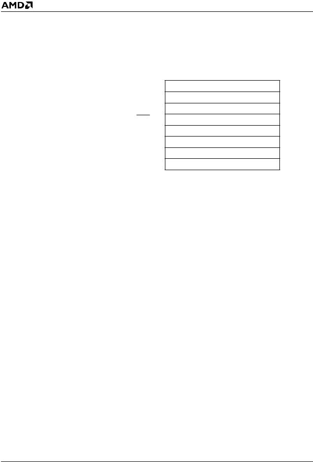
PRODUCT SELECTOR GUIDE
|
Family Part No: |
|
|
Am29F040 |
|
|
||||||
|
|
|
|
|
|
|
||||||
|
Ordering Part No: VCC = 5.0 V ± 5% |
-55 |
|
|
|
|
||||||
|
|
|
|
|
|
|
|
|
|
|
|
|
|
|
|
|
|
|
|
VCC = 5.0 V ± 10% |
|
-70 |
-90 |
-120 |
-150 |
|
|
|
|
|
|
|
||||||
|
Max Access Time (ns) |
55 |
70 |
90 |
120 |
150 |
||||||
|
|
|
|
|
|
|
|
|
|
|
|
|
|
|
|
|
|
|
|
|
55 |
70 |
90 |
120 |
150 |
|
CE |
(E) Access (ns) |
||||||||||
|
|
|
|
|
|
|
|
|
|
|||
|
|
|
|
|
|
Access (ns) |
25 |
30 |
35 |
50 |
55 |
|
|
OE |
(G) |
||||||||||
|
|
|
|
|
|
|
|
|
|
|
|
|
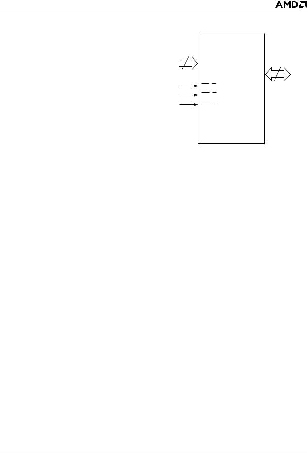
BLOCK DIAGRAM |
|
|
|
|
|
|
|
|
|
|
|
|
DQ0–DQ7 |
VCC |
|
|
|
|
|
|
VSS |
|
Erase Voltage |
|
|
Input/Output |
|
|
|
|
Generator |
|
|
Buffers |
WE |
State |
|
|
|
|
|
Control |
|
|
|
|
|
|
|
|
|
|
|
|
|
|
Command |
PGM Voltage |
|
|
|
|
|
Register |
|
|
|
|
|
|
|
Generator |
Chip Enable |
|
|
|
|
|
|
STB |
Data Latch |
||
CE |
|
|
Output Enable |
|||
|
|
|
|
|||
OE |
|
|
|
Logic |
|
|
|
|
|
STB |
Y-Decoder |
|
Y-Gating |
|
|
|
|
|
|
|
|
VCC Detector |
Timer |
Latch |
|
|
|
|
|
|
|
|
|
|
|
|
|
Address |
X-Decoder |
|
Cell Matrix |
A0–A18 |
|
|
|
|
|
|
|
|
|
|
|
|
|
17113E-2
Am29F040 |
3 |
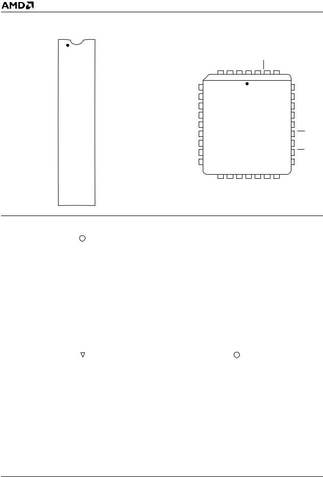
CONNECTION DIAGRAMS
|
|
PDIP |
|
|
|
|
|
A18 |
|
|
|
|
VCC |
||
1 |
32 |
||||||
A16 |
|
|
|
WE |
|||
2 |
31 |
||||||
A15 |
|
|
|
|
A17 |
||
3 |
30 |
||||||
A12 |
|
|
|
A14 |
|||
4 |
29 |
||||||
A7 |
|
|
|
|
A13 |
||
5 |
28 |
||||||
A6 |
|
|
|
A8 |
|||
6 |
27 |
||||||
A5 |
|
|
|
A9 |
|||
7 |
26 |
||||||
A4 |
|
|
|
A11 |
|||
8 |
25 |
||||||
A3 |
|
|
|
|
|
|
|
9 |
24 |
|
OE |
||||
A2 |
|
|
|
A10 |
|||
10 |
23 |
||||||
A1 |
|
|
|
|
|
||
11 |
22 |
|
CE |
||||
A0 |
|
|
|
DQ7 |
|||
12 |
21 |
||||||
DQ0 |
|
|
|
|
DQ6 |
||
13 |
20 |
||||||
DQ1 |
|
|
|
DQ5 |
|||
14 |
19 |
||||||
DQ2 |
|
|
|
|
DQ4 |
||
15 |
18 |
||||||
VSS |
|
|
|
DQ3 |
|||
16 |
17 |
||||||
|
|
|
PLCC |
|
|
|
|
|
|
A12 |
A15 |
A16 |
A18 |
CC |
WE |
A17 |
|
|
V |
|
||||||
|
4 |
3 |
2 |
1 |
32 31 30 |
|
||
A7 |
5 |
|
|
|
|
|
29 |
A14 |
A6 |
6 |
|
|
|
|
|
28 |
A13 |
A5 |
7 |
|
|
|
|
|
27 |
A8 |
A4 |
8 |
|
|
|
|
|
26 |
A9 |
A3 |
9 |
|
|
|
|
|
25 |
A11 |
A2 |
10 |
|
|
|
|
|
24 |
OE |
A1 |
11 |
|
|
|
|
|
23 |
A10 |
A0 |
12 |
|
|
|
|
|
22 |
CE |
DQ0 |
13 |
|
|
|
|
|
21 |
DQ7 |
|
14 15 16 17 18 19 20 |
|
||||||
|
DQ1 |
DQ2 |
V |
DQ3 |
DQ4 |
DQ5 |
DQ6 |
|
|
|
|
SS |
|
|
|
|
|
17113E-3 |
|
|
|
|
|
|
|
17113E-4 |
|
|
|
|
|
TSOP |
|
|
|
|
A11 |
|
|
|
|
|
|
|
||
|
1 |
32 |
|
|
OE |
|
|||
|
|
||||||||
|
A9 |
|
2 |
31 |
|
A10 |
|||
|
|
||||||||
|
A8 |
|
3 |
30 |
|
CE |
|||
|
|
||||||||
A13 |
|
4 |
29 |
|
DQ7 |
||||
|
|
||||||||
A14 |
|
5 |
28 |
|
DQ6 |
||||
|
|
||||||||
A17 |
|
6 |
27 |
|
DQ5 |
||||
|
|
||||||||
WE |
|
7 |
26 |
|
DQ4 |
||||
|
|
||||||||
VCC |
|
8 |
25 |
|
DQ3 |
||||
|
|
||||||||
A18 |
|
9 |
24 |
|
VSS |
||||
|
|
||||||||
A16 |
|
10 |
23 |
|
DQ2 |
||||
|
|
||||||||
A15 |
|
11 |
22 |
|
DQ1 |
||||
|
|
||||||||
A12 |
|
12 |
21 |
|
DQ0 |
||||
|
|
||||||||
|
A7 |
|
13 |
20 |
|
A0 |
|||
|
|
||||||||
|
A6 |
|
14 |
19 |
|
A1 |
|||
|
|
||||||||
|
A5 |
|
15 |
18 |
|
A2 |
|||
|
|
||||||||
|
A4 |
|
16 |
17 |
|
A3 |
|||
|
|
||||||||
|
|
|
|
|
29F040 Standard Pinout |
|
|
|
|
|
|
|
|
|
|
|
A11 |
||
|
|
|
|
1 |
32 |
|
|||
OE |
|
|
|||||||
|
|
||||||||
A10 |
|
2 |
31 |
|
A9 |
||||
|
|
||||||||
CE |
|
3 |
30 |
|
A8 |
||||
|
|
||||||||
DQ7 |
|
4 |
29 |
|
A13 |
||||
|
|
||||||||
DQ6 |
|
5 |
28 |
|
A14 |
||||
|
|
||||||||
DQ5 |
|
6 |
27 |
|
A17 |
||||
|
|
||||||||
DQ4 |
|
7 |
26 |
|
WE |
||||
|
|
||||||||
DQ3 |
|
8 |
25 |
|
VCC |
||||
|
|
||||||||
VSS |
|
9 |
24 |
|
A18 |
||||
|
|
||||||||
DQ2 |
|
10 |
23 |
|
A16 |
||||
|
|
||||||||
DQ1 |
|
11 |
22 |
|
A15 |
||||
|
|
||||||||
DQ0 |
|
12 |
21 |
|
A12 |
||||
|
|
||||||||
|
A0 |
|
13 |
20 |
|
A7 |
|||
|
|
||||||||
|
A1 |
|
14 |
19 |
|
A6 |
|||
|
|
||||||||
|
A2 |
|
15 |
18 |
|
A5 |
|||
|
|
||||||||
|
A3 |
|
16 |
17 |
|
A4 |
|||
|
|
||||||||
29F040 Reverse Pinout
17113E-5
4 |
Am29F040 |
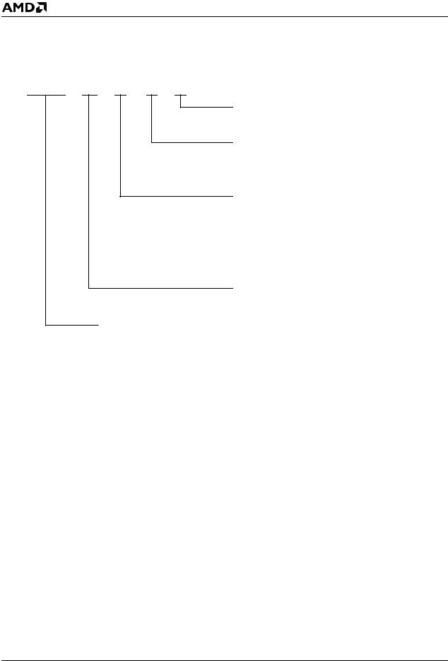
PIN CONFIGURATION
A0–A18 |
= |
Address Inputs |
|||
DQ0–DQ7 = |
Data Input/Output |
||||
|
|
|
|
= |
Chip Enable |
CE |
|||||
|
|
|
= |
Output Enable |
|
OE |
|||||
|
|
= |
Write Enable |
||
WE |
|||||
VSS |
= |
Device Ground |
|||
VCC |
= |
Device Power Supply |
|||
|
|
|
|
|
(5.0 V ±10% or ±5%) |
LOGIC SYMBOL
19
A0–A18 |
8 |
DQ0–DQ7
CE (E)
OE (G)
WE (W)
17113E-6
Am29F040 |
5 |
ORDERING INFORMATION
Standard Products
AMD standard products are available in several packages and operating ranges. The order number (Valid Combination) is formed by a combination of:
AM29F040 |
-55 |
E |
C |
B |
OPTIONAL PROCESSING
Blank = Standard Processing
B = Burn-In
TEMPERATURE RANGE
C = Commercial (0°C to +70°C)
I = Industrial (–40°C to +85°C)
E = Extended (–55°C to +125°C)
PACKAGE TYPE
P = 32-Pin Plastic DIP (PD 032)
J = 32-Pin Rectangular Plastic Leaded Chip
Carrier (PL 032)
E = 32-Pin Thin Small Outline Package (TSOP)
Standard Pinout (TS 032)
F = 32-Pin Thin Small Outline Package (TSOP)
Reverse Pinout (TSR032)
SPEED OPTION
See Product Selector Guide
and Valid Combinations
DEVICE NUMBER/DESCRIPTION
Am29F040
4 Megabit (524,288 x 8-Bit) CMOS 5.0 Volt-only, Sector Erase Flash Memory
|
Valid Combinations |
|
|
|
|
AM29F040-55 |
|
JC, JI, JE, EC, EI, EE, FC, FI, FE |
|
|
|
AM29F040-70 |
|
|
|
|
|
|
|
|
AM29F040-90 |
|
PC, PCB, PI, PIB, PE, PEB, |
|
|
JC, JCB, JI, JIB, JE, JEB, |
AM29F040-120 |
|
|
|
EC, ECB, EI, EIB, EE, EEB, |
|
|
|
|
AM29F040-150 |
|
FC, FCB, FI, FIB, P11 |
|
FE, FEB |
|
|
|
|
|
|
|
Valid Combinations
Valid Combinations list configurations planned to be supported in volume for this device. Consult the local AMD sales office to confirm availability of specific valid combinations and to check on newly released combinations.
6 |
Am29F040 |
Table 1. Am29F040 User Bus Operations
|
|
|
|
|
|
|
|
|
|
|
|
|
|
|
Operation |
|
CE |
|
OE |
WE |
A0 |
A1 |
A6 |
A9 |
I/O |
||||
|
|
|
|
|
|
|
|
|
|
|
|
|
||
Autoselect Manufacturer Code (Note 1) |
|
L |
|
|
L |
|
H |
L |
L |
L |
VID |
Code |
||
Autoselect Device Code (Note 1) |
|
L |
|
|
L |
|
H |
H |
L |
L |
VID |
Code |
||
Read (Note 4) |
|
L |
|
|
L |
|
H |
A0 |
A1 |
A6 |
A9 |
RD |
||
|
|
|
|
|
|
|
|
|
|
|
|
|
||
Standby |
|
H |
|
|
X |
|
X |
X |
X |
X |
X |
HIGH Z |
||
|
|
|
|
|
|
|
|
|
|
|
|
|
||
Output Disable |
|
L |
|
|
H |
|
H |
X |
X |
X |
X |
HIGH Z |
||
|
|
|
|
|
|
|
|
|
|
|
|
|
||
Write |
|
L |
|
|
H |
|
L |
A0 |
A1 |
A6 |
A9 |
PD (Note 2) |
||
|
|
|
|
|
|
|
|
|
|
|
|
|
||
Verify Sector Protect (Note 3) |
|
L |
|
|
L |
|
H |
L |
H |
L |
VID |
Code |
||
Autoselect Device Unprotect Code |
|
L |
|
|
L |
|
H |
H |
H |
L |
VID |
Code |
||
Legend:
L = Logic 0, H = Logic 1, X = Don’t Care. See DC Characteristics for voltage levels.
Notes:
1.Manufacturer and device codes may also be accessed via a command register write sequence. Refer to Tables 2 and 4.
2.Refer to Table 3 for valid PD (Program Data) during a write operation.
3.Refer to the section on Sector Protection.
4.WE can be VIL if OE is VIL, OE at VIH initiates the write operations.
Read Mode
The Am29F040 has two control functions which must be satisfied in order to obtain data at the outputs. CEis the power control and should be used for device selection. OE is the output control and should be used to gate data to the output pins if a device is selected.
Address access time (tACC) is equal to the delay from stable addresses to valid output data. The chip enable access time (tCE) is the delay from stable addresses and
stable CE to valid data at the output pins. The output enable access time is the delay from the falling edge of OE to valid data at the output pins (assuming the addresses have been stable for at least tACC–tOE time).
Standby Mode
The Am29F040 has two standby modes, a CMOS standby mode (CE input held at VCC ± 0.5 V), when the current consumed is less than 5 A; and a TTL standby mode (CE is held at VIH) when the current required is reduced to approximately 1 mA. In the standby mode the outputs are in a high impedance state, independent of the OE input.
If the device is deselected during erasure or programming, the device will draw active current until the operation is completed.
Output Disable
With the OE input at a logic high level (VIH), output from the device is disabled. This will cause the output pins to be in a high impedance state.
Autoselect
The autoselect mode allows the reading out of a binary code from the device and will identify its manufacturer and type. This mode is intended for use by programming equipment for the purpose of automatically matching the device to be programmed with its corresponding programming algorithm. This mode is functional over the entire temperature range of the device.
To activate this mode, the programming equipment must force VID (11.5 V to 12.5 V) on address pin A9. Two identifier bytes may then be sequenced from the device outputs by toggling address A0 from VIL to VIH. All addresses are don’t cares except A0, A1, and A6.
The manufacturer and device codes may also be read via the command register, for instances when the Am29F040 is erased or programmed in a system without access to high voltage on the A9 pin. The command sequence is illustrated in Table 4 (refer to Autoselect Command section).
Byte 0 (A0 = VIL) represents the manufacturer’s code (AMD = 01H) and byte 1 (A0 = VIH) the device identifier code (Am29F040 = A4H). All identifiers for manufacturer and device exhibit odd parity with the MSB (DQ7) defined as the parity bit. See Table 2.
Am29F040 |
7 |

Table 2. Am29F040 Autoselect Codes
|
|
|
|
|
|
|
Code |
|
|
|
|
|
|
|
|
Type |
A18 |
A17 |
A16 |
A6 |
A1 |
A0 |
(HEX) |
DQ7 |
DQ6 |
DQ5 |
DQ4 |
DQ3 |
DQ2 |
DQ1 |
DQ0 |
|
|
|
|
|
|
|
|
|
|
|
|
|
|
|
|
Manufacturer |
X |
X |
X |
VIL |
VIL |
VIL |
01H |
0 |
0 |
0 |
0 |
0 |
0 |
0 |
1 |
ID |
|||||||||||||||
Am29F040 |
X |
X |
X |
VIL |
VIL |
VIH |
A4H |
1 |
0 |
1 |
0 |
0 |
1 |
0 |
0 |
Device ID |
|||||||||||||||
Sector |
Sector Addresses |
VIL |
VIH |
VIL |
01H* |
0 |
0 |
0 |
0 |
0 |
0 |
0 |
1 |
||
Protection |
|||||||||||||||
*Outputs 01H at protected sector addresses
|
Table 3. |
Sector Addresses |
|||
|
|
|
|
|
|
|
A18 |
|
A17 |
A16 |
Address Range |
|
|
|
|
|
|
SA0 |
0 |
|
0 |
0 |
00000h–0FFFFh |
|
|
|
|
|
|
SA1 |
0 |
|
0 |
1 |
10000h–1FFFFh |
|
|
|
|
|
|
SA2 |
0 |
|
1 |
0 |
20000h–2FFFFh |
|
|
|
|
|
|
SA3 |
0 |
|
1 |
1 |
30000h–3FFFFh |
|
|
|
|
|
|
SA4 |
1 |
|
0 |
0 |
40000h–4FFFFh |
|
|
|
|
|
|
SA5 |
1 |
|
0 |
1 |
50000h–5FFFFh |
|
|
|
|
|
|
SA6 |
1 |
|
1 |
0 |
60000h–6FFFFh |
|
|
|
|
|
|
SA7 |
1 |
|
1 |
1 |
70000h–7FFFFh |
|
|
|
|
|
|
Write
Device erasure and programming are accomplished via the command register. The contents of the register serve as inputs to the internal state machine. The state machine outputs dictate the function of the device.
The command register itself does not occupy any addressable memory location. The register is a latch used to store the commands, along with the address and data information needed to execute the command. The command register is written by bringing WE to VIL,
while CE is at VIL and OE is at VIH. Addresses are
latched on the falling edge of WE or CE, whichever happens later; while data is latched on the rising edge of WE or CE, whichever happens first. Standard microprocessor write timings are used.
Refer to AC Write Characteristics and the Erase/ Programming Waveforms for specific timing parameters.
Sector Protection
The Am29F040 features hardware sector protection. This feature will disable both program and erase operations in any number of sectors (0 through 8). The sector protect feature is enabled using programming equipment at the user’s site. The device is shipped with all sectors unprotected. Alternatively, AMD may program and protect sectors in the factory prior to shipping the device (AMD’s ExpressFlash™ Service).
It is also possible to determine if a sector is protected in the system by writing an Autoselect command. Performing a read operation at the address location XX02H, where the higher order addresses (A16, A17, and A18) are used to select the desired sector.
The device produces a logical “1” at DQ0 for a protected sector and a logical “0” for an unprotected sector. See Table 2 for Autoselect codes.
Sector Unprotect
The Am29F040 also features a sector unprotect mode so that a protected sector may be unprotected to incorporate any changes in the code. The sector unprotect is enabled using programming equipment at the user’s site.
Command Definitions
Device operations are selected by writing specific address and data sequences into the command register. Writing incorrect address and data values or writing them in the improper sequence will reset the device to read mode. Table 4 defines the valid register command sequences. Note that the Erase Suspend (B0) and Erase Resume (30) commands are valid only while the Sector Erase operation is in progress. Either of the two reset commands will reset the device (when applicable).
8 |
Am29F040 |

Table 4. Am29F040 Command Definitions
|
Bus |
|
|
|
|
|
|
Fourth Bus |
|
|
|
|
||
|
First Bus |
Second Bus |
Third Bus |
Read/Write |
Fifth Bus |
Sixth Bus |
||||||||
Command |
Write |
|||||||||||||
Write Cycle |
Write Cycle |
Write Cycle |
Cycle |
Write Cycle |
Write Cycle |
|||||||||
Sequence |
Cycles |
|||||||||||||
|
|
|
|
|
|
|
|
|
|
|
|
|||
Read/Reset |
Req’d |
Addr |
Data |
Addr |
Data |
Addr |
Data |
Addr |
Data |
Addr |
Data |
Addr |
Data |
|
|
|
|
|
|
|
|
|
|
|
|
|
|
|
|
Read/Reset |
1 |
XXXXH |
F0H |
|
|
|
|
|
|
|
|
|
|
|
|
|
|
|
|
|
|
|
|
|
|
|
|
|
|
Read/Reset |
4 |
5555H |
AAH |
2AAAH |
55H |
5555H |
F0H |
RA |
RD |
|
|
|
|
|
|
|
|
|
|
|
|
|
|
|
|
|
|
|
|
Autoselect |
4 |
5555H |
AAH |
2AAAH |
55H |
5555H |
90H |
00H |
01H |
|
|
|
|
|
|
|
|
|
|
|
|||||||||
01H |
A4H |
|
|
|
|
|||||||||
|
|
|
|
|
|
|
|
|
|
|
|
|||
|
|
|
|
|
|
|
|
|
|
|
|
|
|
|
Byte Program |
4 |
5555H |
AAH |
2AAAH |
55H |
5555H |
A0H |
PA |
PD |
|
|
|
|
|
|
|
|
|
|
|
|
|
|
|
|
|
|
|
|
Chip Erase |
6 |
5555H |
AAH |
2AAAH |
55H |
5555H |
80H |
5555H |
AAH |
2AAAH |
55H |
5555H |
10H |
|
|
|
|
|
|
|
|
|
|
|
|
|
|
|
|
Sector Erase |
6 |
5555H |
AAH |
2AAAH |
55H |
5555H |
80H |
5555H |
AAH |
2AAAH |
55H |
SA |
30H |
|
|
|
|
|
|
|
|
|
|
|
|
|
|
|
|
Sector Erase Suspend |
Erase can be suspended during sector erase with Addr (don’t care), Data (B0H) |
|
|
|||||||||||
|
|
|
|
|
||||||||||
Sector Erase Resume |
Erase can be resumed after suspend with Addr (don’t care), Data (30H) |
|
|
|
||||||||||
|
|
|
|
|
|
|
|
|
|
|
|
|
|
|
Notes:
1.Address bits A15, A16, A17, and A18 = X = Don’t Care for all address commands except for Program Address (PA), Sector Address (SA), Read Address (RA), and autoselect sector protect verify.
2.Bus operations are defined in Table 1.
3.RA = Address of the memory location to be read.
PA = Address of the memory location to be programmed. Addresses are latched on the falling edge of the WEpulse.
SA = Address of the sector to be erased. The combination of A18, A17, A16 will uniquely select any sector (see Table 3).
4.RD = Data read from location RA during read operation.
PD = Data to be programmed at location PA. Data is latched on the rising edge of WE.
5.Read from non-erasing sectors is allowed in the Erase Suspend mode.
Read/Reset Command
The read or reset operation is initiated by writing the read/reset command sequence into the command register. Microprocessor read cycles retrieve array data from the memory. The device remains enabled for reads until the command register contents are altered.
The device will automatically power-up in the read/ reset state. In this case, a command sequence is not required to read data. Standard microprocessor read cycles will retrieve array data. This default value ensures that no spurious alteration of the memory content occurs during the power transition. Refer to the AC Read Characteristics and Waveforms for the specific timing parameters.
Autoselect Command
Flash memories are intended for use in applications where the local CPU alters memory contents. As such, manufacture and device codes must be accessible while the device resides in the target system. PROM programmers typically access the signature codes by raising A9 to a high voltage. However, multiplexing high voltage onto the address lines is not generally desired system design practice.
The device contains a command autoselect operation to supplement traditional PROM programming methodology. The operation is initiated by writing the autoselect command sequence into the command register. Following the command write, a read cycle from address XX00H retrieves the manufacture code of 01H. A read cycle from address XX01H returns the device code A4H (see Table 2). All manufacturer and device codes will exhibit odd parity with the MSB (DQ7) defined as the parity bit.
Scanning the sector addresses (A16, A17, A18) while (A6, A1, A0) = (0, 1, 0) will produce a logical “1” at device output DQ0 for a protected sector.
To terminate the operation, it is necessary to write the read/reset command sequence into the register.
Byte Programming
The device is programmed on a byte-by-byte basis. Programming is a four bus cycle operation. There are two “unlock” write cycles. These are followed by the program setup command and data write cycles. Addresses are latched on the falling edge of CE or WE, whichever happens later and the data is latched on the rising edge of CE or WE, whichever happens first. The
Am29F040 |
9 |

rising edge of CE or WE (whichever happens first) begins programming. Upon executing the Embedded Program Algorithm command sequence the system is not required to provide further controls or timings. The device will automatically provide adequate internally generated program pulses and verify the programmed cell margin.
The automatic programming operation is completed when the data on DQ7 is equivalent to data written to this bit (see Write Operation Status section) at which time the device returns to the read mode and addresses are no longer latched. Therefore, the device requires that a valid address to the device be supplied by the system at this particular instance of time. Hence, Data Polling must be performed at the memory location which is being programmed.
Any commands written to the chip during this period will be ignored.
Programming is allowed in any sequence and across sector boundaries. Beware that a data “0” cannot be programmed back to a “1”. Attempting to do so may cause the device to exceed programming time limits (DQ5 = 1) or result in an apparent success, according to the data polling algorithm, but a read from reset/read mode will show that the data is still “0”. Only erase operations can convert “0”s to “1”s.
Figure 1 illustrates the Embedded Programming Algorithm using typical command strings and bus operations.
Chip Erase
Chip erase is a six bus cycle operation. There are two “unlock” write cycles. These are followed by writing the “setup” command. Two more “unlock” write cycles are then followed by the chip erase command.
Chip erase does not require the user to program the device prior to erase. Upon executing the Embedded Erase Algorithm command sequence the device automatically will program and verify the entire memory for an all zero data pattern prior to electrical erase. The chip erase is performed sequentially one sector at a time. The system is not required to provide any controls or timings during these operations.
The automatic erase begins on the rising edge of the last WE pulse in the command sequence and terminates when the data on DQ7 is “1” (see Write Operation Status section) at which time the device returns to read the mode.
Figure 2 illustrates the Embedded Erase Algorithm using typical command strings and bus operations.
Sector Erase
Sector erase is a six bus cycle operation. There are two “unlock” write cycles. These are followed by writing the “setup” command. Two more “unlock” write cycles are then followed by the sector erase command. The sector address (any address location within the desired sector)
is latched on the falling edge of WE, while the command (data) is latched on the rising edge of WE. A time-out of 80 s from the rising edge of the last sector erase command will initiate the sector erase command(s).
Multiple sectors may be erased concurrently by writing the six bus cycle operations as described above. This sequence is followed with writes of the Sector Erase command to addresses in other sectors desired to be concurrently erased. The time between writes must be less than 80 s, otherwise that command will not be accepted. It is recommended that processor interrupts be disabled during this time to guarantee this condition. The interrupts can be re-enabled after the last Sector Erase command is written. A time-out of 80 s from the rising edge of the last WE will initiate the execution of the Sector Erase command(s). If another falling edge of the WE occurs within the 80 s time-out window the timer is reset. (Monitor DQ3 to determine if the sector erase window is still open, see section DQ3, Sector Erase Timer.) Any command other than Sector Erase or Erase Suspend during this period resets the device to read mode, ignoring the previous command string. In that case, restart the erase on those sectors and allow them to complete. (Refer to the Write Operation Status section for Sector Erase Timer operation.) Loading the sector erase buffer may be done in any sequence and with any number of sectors (1 to 8).
Sector erase does not require the user to program the device prior to erase. The device automatically programs all memory locations in the sector(s) to be erased prior to electrical erase. When erasing a sector or sectors the remaining unselected sectors are not affected. The system is not required to provide any controls or timings during these operations.
The automatic sector erase begins after the 80 s time out from the rising edge of the WE pulse for the last sector erase command pulse and terminates when the data on DQ7 is “1" (see Write Operation Status section) at which time the device returns to read mode. During the execution of the Sector Erase command, only the Erase Suspend and Erase Resume commands are allowed. All other commands will be ignored. Data polling must be performed at an address within any of the sectors being erased.
Figure 2 illustrates the Embedded Erase Algorithm using typical command strings and bus operations.
10 |
Am29F040 |
 Loading...