


AMD Advanced Micro Devices AM29F002T-70PC, AM29F002T-70JIB, AM29F002T-70JI, AM29F002T-70JC, AM29F002T-70EIB Datasheet
...PRELIMINARY
Am29F002/Am29F002N
2 Megabit (256 K x 8-Bit)
CMOS 5.0 Volt-only Boot Sector Flash Memory
DISTINCTIVE CHARACTERISTICS
■Single power supply operation
—5.0 Volt-only operation for read, erase, and program operations
—Minimizes system level requirements
■High performance
—Access times as fast as 55 ns
■Low power consumption (typical values at 5 MHz)
—1 µA standby mode current
—20 mA read current
—30 mA program/erase current
■Flexible sector architecture
—One 16 Kbyte, two 8 Kbyte, one 32 Kbyte, and three 64 Kbyte sectors
—Supports full chip erase
—Sector Protection features:
A hardware method of locking a sector to prevent any program or erase operations within that sector
Sectors can be locked via programming equipment
Temporary Sector Unprotect feature allows code changes in previously locked sectors
■Top or bottom boot block configurations available
■Embedded Algorithms
—Embedded Erase algorithm automatically preprograms and erases the entire chip or any combination of designated sectors
—Embedded Program algorithm automatically writes and verifies data at specified addresses
■Minimum 100,000 write cycle guarantee per sector
■Package option
—32-pin PDIP
—32-pin TSOP
—32-pin PLCC
■Compatibility with JEDEC standards
—Pinout and software compatible with singlepower supply Flash
—Superior inadvertent write protection
■Data# Polling and toggle bits
—Provides a software method of detecting program or erase operation completion
■Erase Suspend/Erase Resume
—Suspends an erase operation to read data from, or program data to, a sector that is not being erased, then resumes the erase operation
■Hardware reset pin (RESET#)
—Hardware method to reset the device to reading array data (not available on Am29F002N)
Publication# 20818 Rev: C Amendment/+2
Issue Date: March 1998

P R E L I M I N A R Y
GENERAL DESCRIPTION
The Am29F002 Family consists of 2 Mbit, 5.0 volt-only Flash memory devices organized as 262,144 bytes. The Am29F002 offers the RESET# function, the Am29F002N does not. The data appears on DQ7– DQ0. The device is offered in 32-pin PLCC, 32-pin TSOP, and 32-pin PDIP packages. This device is designed to be programmed in-system with the standard system 5.0 volt VCC supply. No VPP is required for write or erase operations. The device can also be programmed in standard EPROM programmers.
The standard device offers access times of 55, 70, 90, and 120 ns, allowing high speed microprocessors to operate without wait states. To eliminate bus contention the device has separate chip enable (CE#), write enable (WE#) and output enable (OE#) controls.
The device requires only a single 5.0 volt power supply for both read and write functions. Internally generated and regulated voltages are provided for the program and erase operations.
The device is entirely command set compatible with the
JEDEC single-power-supply Flash standard. Commands are written to the command register using standard microprocessor write timings. Register contents serve as input to an internal state-machine that controls the erase and programming circuitry. Write cycles also internally latch addresses and data needed for the programming and erase operations. Reading data out of the device is similar to reading from other Flash or EPROM devices.
Device programming occurs by executing the program command sequence. This initiates the Embedded Program algorithm—an internal algorithm that automatically times the program pulse widths and verifies proper cell margin.
Device erasure occurs by executing the erase command sequence. This initiates the Embedded Erase algorithm—an internal algorithm that automatically preprograms the array (if it is not already programmed) before executing the erase operation. During erase, the
device automatically times the erase pulse widths and verifies proper cell margin.
The host system can detect whether a program or erase operation is complete by reading the DQ7 (Data# Polling) and DQ6 (toggle) status bits. After a program or erase cycle has been completed, the device is ready to read array data or accept another command.
The sector erase architecture allows memory sectors to be erased and reprogrammed without affecting the data contents of other sectors. The device is fully erased when shipped from the factory.
Hardware data protection measures include a low VCC detector that automatically inhibits write operations during power transitions. The hardware sector protection feature disables both program and erase operations in any combination of the sectors of memory. This can be achieved via programming equipment.
The Erase Suspend feature enables the user to put erase on hold for any period of time to read data from, or program data to, any sector that is not selected for erasure. True background erase can thus be achieved.
The hardware RESET# pin terminates any operation in progress and resets the internal state machine to reading array data. The RESET# pin may be tied to the system reset circuitry. A system reset would thus also reset the device, enabling the system microprocessor to read the boot-up firmware from the Flash memory. (This feature is not available on the Am29F002N.)
The system can place the device into the standby mode. Power consumption is greatly reduced in this mode.
AMD’s Flash technology combines years of Flash memory manufacturing experience to produce the highest levels of quality, reliability and cost effectiveness. The device electrically erases all bits within a sector simultaneously via Fowler-Nordheim tunneling. The data is programmed using hot electron injection.
2 |
Am29F002/Am29F002N |

P R E L I M I N A R Y
PRODUCT SELECTOR GUIDE
Family Part Number |
|
Am29F002/Am29F002N |
|
||
|
|
|
|
|
|
Speed Option |
VCC = 5.0 V ± 5% |
-55 |
|
|
|
|
|
|
|
|
|
VCC = 5.0 V ± 10% |
|
-70 |
-90 |
-120 |
|
|
|
||||
|
|
|
|
|
|
Max access time, ns (tACC) |
55 |
70 |
90 |
120 |
|
|
|
|
|
|
|
Max CE# access time, ns (tCE) |
55 |
70 |
90 |
120 |
|
|
|
|
|
|
|
Max OE# access time, ns (tOE) |
30 |
30 |
35 |
50 |
|
|
|
|
|
|
|
Note: See “AC Characteristics” for full specifications.
BLOCK DIAGRAM
|
|
|
|
|
|
DQ0–DQ7 |
VCC |
|
|
Sector Switches |
|
|
|
VSS |
|
|
|
|
|
|
|
|
|
|
|
|
|
RESET# |
|
|
Erase Voltage |
|
|
Input/Output |
|
|
Generator |
|
|
Buffers |
|
|
|
|
|
|
||
n/a Am29F00N |
|
|
|
|
|
|
WE# |
State |
|
|
|
|
|
|
Control |
|
|
|
|
|
|
Command |
|
|
|
|
|
|
Register |
PGM Voltage |
|
|
|
|
|
|
Generator |
|
|
|
|
|
|
|
Chip Enable |
STB |
Data |
|
|
|
|
Latch |
|||
CE# |
|
|
Output Enable |
|||
|
|
|
|
|||
OE# |
|
|
|
Logic |
|
|
|
|
|
|
|
|
|
|
|
|
STB |
Y-Decoder |
|
Y-Gating |
|
|
|
|
|
|
|
|
VCC Detector |
Timer |
Latch |
|
|
|
|
|
|
|
|
|
|
|
|
|
Address |
X-Decoder |
|
Cell Matrix |
A0–A17 |
|
|
|
|
|
|
|
|
|
|
|
|
|
|
|
|
|
|
|
20818C-1 |
Am29F002/Am29F002N |
3 |
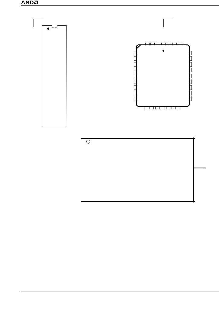
CONNECTION DIAGRAMS
NC on Am29F00N
RESET#NC |
|
1 |
|
32 |
|
|
VCC |
|
|
|
|
|
|
|
|
|
|
A16 |
|
2 |
|
31 |
|
|
WE# |
|
|
|
|
|
|
|
|
|
|
A15 |
|
3 |
|
30 |
|
|
A17 |
|
|
|
|
|
|
|
|
|
|
A12 |
|
4 |
|
29 |
|
|
A14 |
|
|
|
|
|
|
|
|
|
|
A7 |
|
5 |
|
28 |
|
|
A13 |
|
|
|
|
|
|
|
|
|
|
A6 |
|
6 |
|
27 |
|
|
A8 |
|
|
|
|
|
|
|
|
|
|
A5 |
|
7 |
|
26 |
|
|
A9 |
|
|
|
|
|
|
|
|
|
|
A4 |
|
8 |
PDIP |
25 |
|
|
A11 |
|
|
|
|
|
|
|
|
|
|
A3 |
|
9 |
|
24 |
|
|
OE# |
|
|
|
|
|
|
|
|
|
|
A2 |
|
10 |
|
23 |
|
|
A10 |
|
|
|
|
|
|
|
|
|
|
A1 |
|
11 |
|
22 |
|
|
CE# |
|
|
|
|
|
|
|
|
|
|
A0 |
|
12 |
|
21 |
|
|
DQ7 |
|
DQ0 |
|
|
|
|
|
|
DQ6 |
|
|
13 |
|
20 |
|
|
|||
|
|
|
|
|
|
|
|
|
DQ1 |
|
14 |
|
19 |
|
|
DQ5 |
|
|
|
|
|
|
|
|
|
|
DQ2 |
|
15 |
|
18 |
|
|
DQ4 |
|
VSS |
|
|
|
|
|
|
|
|
|
16 |
|
17 |
|
|
DQ3 |
||
|
|
|
|
A11 |
|
|
1 |
|
|
|
|
|
|
|
|
||
|
|
|
|
|
|
|
||
|
|
|
|
A9 |
|
|
2 |
|
|
|
|
|
|
|
|
||
|
|
|
|
A8 |
|
|
3 |
|
|
|
|
|
|
|
|
||
|
|
|
|
A13 |
|
|
4 |
|
|
|
|
|
|
|
|
||
|
|
|
|
A14 |
|
|
|
5 |
|
|
|
|
|
|
|
||
|
|
|
|
A17 |
|
|
6 |
|
|
|
|
|
|
|
|
||
|
|
|
|
WE# |
|
|
7 |
|
|
|
|
|
VCC |
|
|
8 |
|
|
|
|
|
|
|
|
||
NC on Am29F00N RESET# |
|
|
9 |
|||||
|
|
|
||||||
|
|
|
|
A16 |
|
|
10 |
|
|
|
|
|
|
|
|
||
|
|
|
|
A15 |
|
|
11 |
|
|
|
|
|
A12 |
|
|
12 |
|
|
|
|
|
|
|
|
||
|
|
|
|
A7 |
|
|
13 |
|
|
|
|
|
|
|
|
||
|
|
|
|
A6 |
|
|
14 |
|
|
|
|
|
|
|
|
||
|
|
|
|
A5 |
|
|
15 |
|
|
|
|
|
|
|
|
||
|
|
|
|
A4 |
|
|
16 |
|
|
|
|
|
|
|
|
||
|
|
|
|
|
|
|
|
|
P R E L I M I N A R Y
NC on Am29F00N
|
|
|
A12 |
A15 |
A16 |
RESET# |
V |
WE# |
A17 |
|
|
|
|
|
|
|
|
CC |
|
|
|
|
|
|
3 |
2 |
1 |
32 31 30 |
|
|||
|
|
|
4 |
|
||||||
A7 |
5 |
|
|
|
|
|
|
29 |
A14 |
|
A6 |
6 |
|
|
|
|
|
28 |
A13 |
||
A5 |
7 |
|
|
|
|
|
27 |
A8 |
||
A4 |
8 |
|
|
|
|
|
26 |
A9 |
||
A3 |
9 |
|
PLCC |
|
25 |
A11 |
||||
A2 |
10 |
|
|
|
|
|
24 |
OE# |
||
A1 |
11 |
|
|
|
|
|
23 |
A10 |
||
A0 |
12 |
|
|
|
|
|
22 |
CE# |
||
DQ0 |
13 |
|
|
|
|
|
21 |
DQ7 |
||
|
14 15 16 17 18 19 20 |
|
||||||||
|
|
|
DQ1 |
DQ2 |
V |
DQ3 |
DQ4 |
DQ5 |
DQ6 |
|
|
|
|
|
|
SS |
|
|
|
|
|
32  OE#
OE#
31  A10
A10
30  CE#
CE#
29  DQ7
DQ7
28  DQ6
DQ6
27  DQ5
DQ5
26  DQ4
DQ4
Standard TSOP 25 DQ3 24  VSS
VSS
23  DQ2
DQ2
22  DQ1
DQ1
21  DQ0
DQ0
20  A0
A0
19  A1
A1
18  A2
A2
17  A3
A3
20818C-2
4 |
Am29F002/Am29F002N |
P R E L I M I N A R Y
PIN CONFIGURATION
A0–A17 |
= |
18 addresses |
DQ0–DQ7 |
= |
8 data inputs/outputs |
CE# |
= |
Chip enable |
OE# |
= |
Output enable |
WE# |
= |
Write enable |
RESET# |
= Hardware reset pin, active low |
|
|
|
(not available on Am29F002N) |
VCC |
= +5.0 V single power supply |
|
|
|
(see Product Selector Guide for |
|
|
device speed ratings and voltage |
|
|
supply tolerances) |
VSS |
= |
Device ground |
NC |
= Pin not connected internally |
|
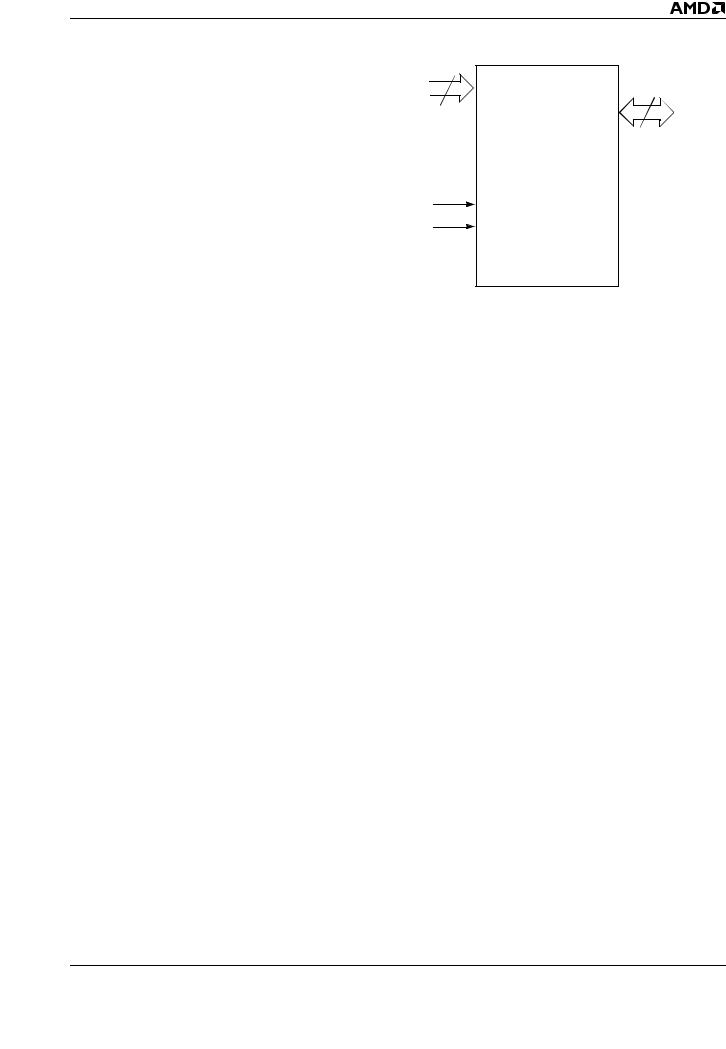
LOGIC SYMBOL
18 |
|
A0–A17 |
8 |
DQ0–DQ7
 CE#
CE#
 OE#
OE#
WE#
RESET#
N/C on Am29F002N
20818C-3
Am29F002/Am29F002N |
5 |
P R E L I M I N A R Y
ORDERING INFORMATION
Standard Product
AMD standard products are available in several packages and operating ranges. The order number (Valid Combination) is formed by a combination of the elements below.
Am29F002 |
T |
-70 |
P |
C |
B |
OPTIONAL PROCESSING
Blank = Standard Processing
B = Burn-In
Contact an AMD representative for more information.
TEMPERATURE RANGE
C = Commercial (0°C to +70°C)
I = Industrial (-40°C to +85°C)
E = Extended (–55°C to +125°C)
PACKAGE TYPE
P = 32-Pin Plastic DIP (PD 032)
J = 32-Pin Rectangular Plastic Leaded Chip
Carrier (PL 032)
E = 32-Pin Thin Small Outline Package
(TSOP) Standard Pinout (TS 032)
SPEED OPTION
See Product Selector Guide and
Valid Combinations
BOOT CODE SECTOR ARCHITECTURE
T = Top sector
B = Bottom sector
DEVICE NUMBER/DESCRIPTION
Am29F002/Am29F002N
2 Megabit (256 K x 8-Bit) CMOS Flash Memory
5.0 Volt-only Program and Erase
Valid Combinations
Am29F002T-55 |
|
|
Am29F002B-55 |
PC, JC, JI, EC, EI |
|
Am29F002NT-55 |
||
|
||
Am29F002NB-55 |
|
|
|
|
|
Am29F002T-70 |
|
|
Am29F002B-70 |
PC, PI, JC, JI, EC, EI |
|
Am29F002NT-70 |
||
|
||
Am29F002NB-70 |
|
|
|
|
|
Am29F002T-90 |
|
|
Am29F002B-90 |
|
|
Am29F002NT-90 |
PC, PI, PE, |
|
Am29F002NB-90 |
||
|
JC, JI, JE, |
|
Am29F002T-120 |
||
EC, EI, EE |
||
Am29F002B-120 |
|
|
Am29F002NT-120 |
|
|
Am29F002NB-120 |
|
|
|
|
Valid Combinations
Valid Combinations list configurations planned to be supported in volume for this device. Consult the local AMD sales office to confirm availability of specific valid combinations and to check on newly released combinations.
6 |
Am29F002/Am29F002N |

P R E L I M I N A R Y
DEVICE BUS OPERATIONS
This section describes the requirements and use of the device bus operations, which are initiated through the internal command register. The command register itself does not occupy any addressable memory location. The register is composed of latches that store the commands, along with the address and data information needed to execute the command. The contents of
the register serve as inputs to the internal state machine. The state machine outputs dictate the function of the device. The appropriate device bus operations table lists the inputs and control levels required, and the resulting output. The following subsections describe each of these operations in further detail.
Table 1. Am29F002/Am29F002N Device Bus Operations
|
|
|
|
RESET# |
|
|
Operation |
CE# |
OE# |
WE# |
(n/a Am29F002N) |
A0–A17 |
DQ0–DQ7 |
|
|
|
|
|
|
|
Read |
L |
L |
H |
H |
AIN |
DOUT |
Write |
L |
H |
L |
H |
AIN |
DIN |
CMOS Standby |
VCC ± 0.5 V |
X |
X |
H |
X |
High-Z |
TTL Standby |
H |
X |
X |
H |
X |
High-Z |
|
|
|
|
|
|
|
Output Disable |
L |
H |
H |
H |
X |
High-Z |
|
|
|
|
|
|
|
Reset (n/a on Am29F002N) |
X |
X |
X |
L |
X |
High-Z |
|
|
|
|
|
|
|
Temporary Sector Unprotect |
X |
X |
X |
VID |
X |
X |
(See Note) |
Legend:
L = Logic Low = VIL, H = Logic High = VIH, VID = 12.0 ± 0.5 V, X = Don’t Care, DIN = Data In, DOUT = Data Out, AIN = Address In
Note: See the sections on Sector Protection and Temporary Sector Unprotect for more information. This function requires the RESET# pin and is therefore not available on the Am29F002N device.
Requirements for Reading Array Data
To read array data from the outputs, the system must drive the CE# and OE# pins to VIL. CE# is the power control and selects the device. OE# is the output control and gates array data to the output pins. WE# should remain at VIH.
The internal state machine is set for reading array data upon device power-up, or after a hardware reset. This ensures that no spurious alteration of the memory content occurs during the power transition. No command is necessary in this mode to obtain array data. Standard microprocessor read cycles that assert valid addresses on the device address inputs produce valid data on the device data outputs. The device remains enabled for read access until the command register contents are altered.
See “Reading Array Data” for more information. Refer to the AC Read Operations table for timing specifications and to the Read Operations Timings diagram for the timing waveforms. ICC1 in the DC Characteristics table represents the active current specification for reading array data.
Writing Commands/Command Sequences
To write a command or command sequence (which includes programming data to the device and erasing
sectors of memory), the system must drive WE# and CE# to VIL, and OE# to VIH.
An erase operation can erase one sector, multiple sectors, or the entire device. The Sector Address Tables indicate the address space that each sector occupies. A “sector address” consists of the address bits required to uniquely select a sector. See the Command Definitions section for details on erasing a sector or the entire chip, or suspending/resuming the erase operation.
After the system writes the autoselect command sequence, the device enters the autoselect mode. The system can then read autoselect codes from the internal register (which is separate from the memory array) on DQ7–DQ0. Standard read cycle timings apply in this mode. Refer to the “Autoselect Mode” and Autoselect Command Sequence sections for more information.
ICC2 in the DC Characteristics table represents the active current specification for the write mode. The “AC Characteristics” section contains timing specification tables and timing diagrams for write operations.
Program and Erase Operation Status
During an erase or program operation, the system may check the status of the operation by reading the status bits on DQ7–DQ0. Standard read cycle timings and ICC read specifications apply. Refer to “Write Operation
Am29F002/Am29F002N |
7 |

P R E L I M I N A R Y
Status” for more information, and to each AC Characteristics section for timing diagrams.
Standby Mode
When the system is not reading or writing to the device, it can place the device in the standby mode. In this mode, current consumption is greatly reduced, and the outputs are placed in the high impedance state, independent of the OE# input.
The device enters the CMOS standby mode when CE# and RESET# pins (CE# only on the Am29F002N) are both held at VCC ± 0.5 V. (Note that this is a more restricted voltage range than VIH.) The device enters the TTL standby mode when CE# and RESET# pins (CE# only on the Am29F002N) are both held at VIH. The device requires standard access time (tCE) for read access when the device is in either of these standby modes, before it is ready to read data.
The device also enters the standby mode when the RESET# pin is driven low. Refer to the next section, “RESET#: Hardware Reset Pin”.
If the device is deselected during erasure or programming, the device draws active current until the operation is completed.
In the DC Characteristics tables, ICC3 represents the standby current specification.
If the device is deselected during erasure or programming, the device draws active current until the operation is completed.
ICC3 in the DC Characteristics tables represents the standby current specification.
RESET#: Hardware Reset Pin
Note: The RESET# pin is not available on the Am29F002N.
The RESET# pin provides a hardware method of resetting the device to reading array data. When the system drives the RESET# pin low for at least a period of tRP, the device immediately terminates any operation in progress, tristates all data output pins, and ignores all read/write attempts for the duration of the RESET# pulse. The device also resets the internal state machine to reading array data. The operation that was interrupted should be reinitiated once the device is ready to accept another command sequence, to ensure data integrity.
Current is reduced for the duration of the RESET# pulse. When RESET# is held at VIL, the device enters the TTL standby mode; if RESET# is held at VSS ± 0.5 V, the device enters the CMOS standby mode.
The RESET# pin may be tied to the system reset circuitry. A system reset would thus also reset the Flash memory, enabling the system to read the boot-up firmware from the Flash memory.
Refer to the AC Characteristics tables for RESET# parameters and timing diagram.
Output Disable Mode
When the OE# input is at VIH, output from the device is disabled. The output pins are placed in the high impedance state.
Table 2. Am29F002/Am29F002N Top Boot Block Sector Address Table
|
|
|
|
|
|
Sector Size |
Address Range |
Sector |
A17 |
A16 |
A15 |
A14 |
A13 |
(Kbytes) |
(in hexadecimal) |
|
|
|
|
|
|
|
|
SA0 |
0 |
0 |
X |
X |
X |
64 |
00000h–0FFFFh |
|
|
|
|
|
|
|
|
SA1 |
0 |
1 |
X |
X |
X |
64 |
10000h–1FFFFh |
|
|
|
|
|
|
|
|
SA2 |
1 |
0 |
X |
X |
X |
64 |
20000h–2FFFFh |
|
|
|
|
|
|
|
|
SA3 |
1 |
1 |
0 |
X |
X |
32 |
30000h–37FFFh |
|
|
|
|
|
|
|
|
SA4 |
1 |
1 |
1 |
0 |
0 |
8 |
38000h–39FFFh |
|
|
|
|
|
|
|
|
SA5 |
1 |
1 |
1 |
0 |
1 |
8 |
3A000h–3BFFFh |
|
|
|
|
|
|
|
|
SA6 |
1 |
1 |
1 |
1 |
X |
16 |
3C000h–3FFFFh |
|
|
|
|
|
|
|
|
8 |
Am29F002/Am29F002N |

P R E L I M I N A R Y
Table 3. Am29F002/Am29F002N Bottom Boot Block Sector Address Table
|
|
|
|
|
|
Sector Size |
Address Range |
Sector |
A17 |
A16 |
A15 |
A14 |
A13 |
(Kbytes) |
(in hexadecimal) |
|
|
|
|
|
|
|
|
SA0 |
0 |
0 |
0 |
0 |
X |
16 |
00000h–03FFFh |
|
|
|
|
|
|
|
|
SA1 |
0 |
0 |
0 |
1 |
0 |
8 |
04000h–05FFFh |
|
|
|
|
|
|
|
|
SA2 |
0 |
0 |
0 |
1 |
1 |
8 |
06000h–07FFFh |
|
|
|
|
|
|
|
|
SA3 |
0 |
0 |
1 |
X |
X |
32 |
08000h–0FFFFh |
|
|
|
|
|
|
|
|
SA4 |
0 |
1 |
X |
X |
X |
64 |
10000h–1FFFFh |
|
|
|
|
|
|
|
|
SA5 |
1 |
0 |
X |
X |
X |
64 |
20000h–2FFFFh |
|
|
|
|
|
|
|
|
SA6 |
1 |
1 |
X |
X |
X |
64 |
30000h–3FFFFh |
|
|
|
|
|
|
|
|
Autoselect Mode
The autoselect mode provides manufacturer and device identification, and sector protection verification, through identifier codes output on DQ7–DQ0. This mode is primarily intended for programming equipment to automatically match a device to be programmed with its corresponding programming algorithm. However, the autoselect codes can also be accessed in-system through the command register.
When using programming equipment, the autoselect mode requires VID (11.5 V to 12.5 V) on address pin A9. Address pins A6, A1, and A0 must be as shown in Autoselect Codes (High Voltage Method) table. In addition, when verifying sector protection, the sector ad-
dress must appear on the appropriate highest order address bits. Refer to the corresponding Sector Address Tables. The Command Definitions table shows the remaining address bits that are don’t care. When all necessary bits have been set as required, the programming equipment may then read the corresponding identifier code on DQ7–DQ0.
To access the autoselect codes in-system, the host system can issue the autoselect command via the command register, as shown in the Command Definitions table. This method does not require VID. See “Command Definitions” for details on using the autoselect mode.
Table 4. Am29F002/Am29F002N Autoselect Codes (High Voltage Method)
|
|
|
|
A17 |
A12 |
|
A8 |
|
A5 |
|
|
DQ7 |
|
|
|
|
|
to |
to |
|
to |
|
to |
|
|
to |
|
Description |
CE# |
OE# |
WE# |
A13 |
A10 |
A9 |
A7 |
A6 |
A2 |
A1 |
A0 |
DQ0 |
|
|
|
|
|
|
|
|
|
|
|
|
|
|
|
Manufacturer ID: AMD |
L |
L |
H |
X |
X |
VID |
X |
L |
X |
L |
L |
01h |
|
Device ID: |
L |
L |
H |
|
|
|
|
|
|
|
|
|
|
Am29F002/Am29F002N |
|
|
|
X |
X |
VID |
X |
L |
X |
L |
H |
B0h |
|
L |
L |
H |
|||||||||||
(Top Boot Block) |
|
|
|
|
|
|
|
|
|
||||
|
|
|
|
|
|
|
|
|
|
|
|
|
|
Device ID: |
L |
L |
H |
|
|
|
|
|
|
|
|
|
|
Am29F002/Am29F002N |
|
|
|
X |
X |
VID |
X |
L |
X |
L |
H |
34h |
|
L |
L |
H |
|||||||||||
(Bottom Boot Block) |
|
|
|
|
|
|
|
|
|
||||
|
|
|
|
|
|
|
|
|
|
|
|
|
|
|
|
|
|
|
|
|
|
|
|
|
|
01h |
|
Sector Protection Verification |
L |
L |
H |
SA |
X |
VID |
X |
L |
X |
H |
L |
(protected) |
|
|
|||||||||||||
00h |
|||||||||||||
|
|
|
|
|
|
|
|
|
|
|
|
||
|
|
|
|
|
|
|
|
|
|
|
|
(unprotected) |
|
|
|
|
|
|
|
|
|
|
|
|
|
|
L = Logic Low = VIL, H = Logic High = VIH, SA = Sector Address, X = Don’t care.
Sector Protection/Unprotection
The hardware sector protection feature disables both program and erase operations in any sector. The hardware sector unprotection feature re-enables both program and erase operations in previously protected sectors.
Sector protection/unprotection must be implemented using programming equipment. The procedure requires a high voltage (VID) on address pin A9 and the control pins. Details on this method are provided in the supplements, publication numbers 20819 and 21183.
Am29F002/Am29F002N |
9 |
P R E L I M I N A R Y
Contact an AMD representative to obtain a copy of the appropriate document.
The device is shipped with all sectors unprotected. AMD offers the option of programming and protecting sectors at its factory prior to shipping the device through AMD’s ExpressFlash™ Service. Contact an AMD representative for details.
It is possible to determine whether a sector is protected or unprotected. See “Autoselect Mode” for details.
Temporary Sector Unprotect
Note: This feature requites the RESET# pin and is therefore not available on the Am29F002N.
This feature allows temporary unprotection of previously protected sectors to change data in-system. The Sector Unprotect mode is activated by setting the RESET# pin to VID. During this mode, formerly protected sectors can be programmed or erased by selecting the sector addresses. Once VID is removed from the RESET# pin, all the previously protected sectors are protected again. Figure 1 shows the algorithm, and the Temporary Sector Unprotect diagram shows the timing waveforms, for this feature.
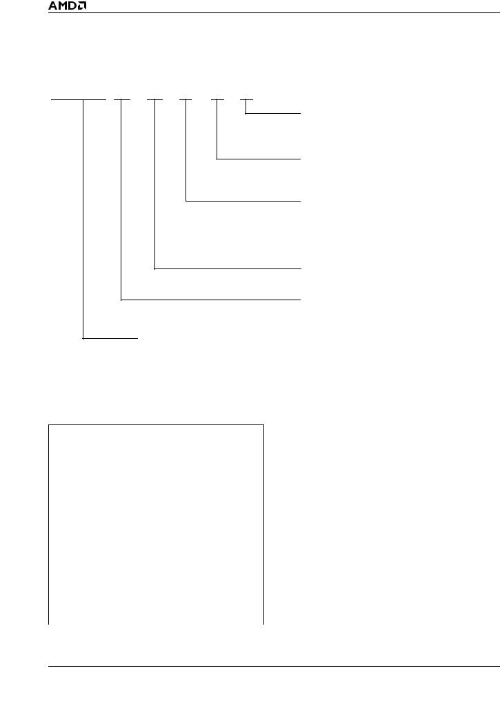
START
RESET# = VID
(Note 1)
Perform Erase or
Program Operations
RESET# = VIH
Temporary Sector
Unprotect
Completed (Note 2)
Hardware Data Protection
The command sequence requirement of unlock cycles for programming or erasing provides data protection against inadvertent writes (refer to the Command Definitions table). In addition, the following hardware data protection measures prevent accidental erasure or programming, which might otherwise be caused by spurious system level signals during VCC power-up and power-down transitions, or from system noise.
Low VCC Write Inhibit
When VCC is less than VLKO, the device does not accept any write cycles. This protects data during VCC
power-up and power-down. The command register and all internal program/erase circuits are disabled, and the device resets. Subsequent writes are ignored until VCC is greater than VLKO. The system must provide the proper signals to the control pins to prevent unintentional writes when VCC is greater than VLKO.
Write Pulse “Glitch” Protection
Noise pulses of less than 5 ns (typical) on OE#, CE# or WE# do not initiate a write cycle.
Logical Inhibit
Write cycles are inhibited by holding any one of OE# = VIL, CE# = VIH or WE# = VIH. To initiate a write cycle, CE# and WE# must be a logical zero while OE# is a logical one.
Power-Up Write Inhibit
If WE# = CE# = VIL and OE# = VIH during power up, the device does not accept commands on the rising edge of WE#. The internal state machine is automatically reset to reading array data on power-up.
20818C-4
Notes:
1.All protected sectors unprotected.
2.All previously protected sectors are protected once again.
Figure 1. Temporary Sector Unprotect Operation
10 |
Am29F002/Am29F002N |
P R E L I M I N A R Y
COMMAND DEFINITIONS
Writing specific address and data commands or sequences into the command register initiates device operations. The Command Definitions table defines the valid register command sequences. Writing incorrect address and data values or writing them in the improper sequence resets the device to reading array data.
All addresses are latched on the falling edge of WE# or CE#, whichever happens later. All data is latched on the rising edge of WE# or CE#, whichever happens first. Refer to the appropriate timing diagrams in the “AC Characteristics” section.
Reading Array Data
The device is automatically set to reading array data after device power-up. No commands are required to retrieve data. The device is also ready to read array data after completing an Embedded Program or Embedded Erase algorithm.
After the device accepts an Erase Suspend command, the device enters the Erase Suspend mode. The system can read array data using the standard read timings, except that if it reads at an address within erasesuspended sectors, the device outputs status data. After completing a programming operation in the Erase Suspend mode, the system may once again read array data with the same exception. See “Erase Suspend/Erase Resume Commands” for more information on this mode.
The system must issue the reset command to re-en- able the device for reading array data if DQ5 goes high, or while in the autoselect mode. See the “Reset Command” section, next.
See also “Requirements for Reading Array Data” in the “Device Bus Operations” section for more information. The Read Operations table provides the read parameters, and Read Operation Timings diagram shows the timing diagram.
Reset Command
Writing the reset command to the device resets the device to reading array data. Address bits are don’t care for this command.
The reset command may be written between the sequence cycles in an erase command sequence before erasing begins. This resets the device to reading array data. Once erasure begins, however, the device ignores reset commands until the operation is complete.
The reset command may be written between the sequence cycles in a program command sequence before programming begins. This resets the device to reading array data (also applies to programming in Erase Suspend mode). Once programming begins,
however, the device ignores reset commands until the operation is complete.
The reset command may be written between the sequence cycles in an autoselect command sequence. Once in the autoselect mode, the reset command must be written to return to reading array data (also applies to autoselect during Erase Suspend).
If DQ5 goes high during a program or erase operation, writing the reset command returns the device to reading array data (also applies during Erase Suspend).
Autoselect Command Sequence
The autoselect command sequence allows the host system to access the manufacturer and devices codes, and determine whether or not a sector is protected. The Command Definitions table shows the address and data requirements. This method is an alternative to that shown in the Autoselect Codes (High Voltage Method) table, which is intended for PROM programmers and requires VID on address bit A9.
The autoselect command sequence is initiated by writing two unlock cycles, followed by the autoselect command. The device then enters the autoselect mode, and the system may read at any address any number of times, without initiating another command sequence.
A read cycle at address XX00h or retrieves the manufacturer code. A read cycle at address XX01h returns the device code. A read cycle containing a sector address (SA) and the address 02h in returns 01h if that sector is protected, or 00h if it is unprotected. Refer to the Sector Address tables for valid sector addresses.
The system must write the reset command to exit the autoselect mode and return to reading array data.
Byte Program Command Sequence
Programming is a four-bus-cycle operation. The program command sequence is initiated by writing two unlock write cycles, followed by the program set-up command. The program address and data are written next, which in turn initiate the Embedded Program algorithm. The system is not required to provide further controls or timings. The device automatically provides internally generated program pulses and verify the programmed cell margin. The Command Definitions take shows the address and data requirements for the byte program command sequence.
When the Embedded Program algorithm is complete, the device then returns to reading array data and addresses are no longer latched. The system can determine the status of the program operation by using DQ7 or DQ6. See “Write Operation Status” for information on these status bits.
Am29F002/Am29F002N |
11 |

P R E L I M I N A R Y
Any commands written to the device during the Embedded Program Algorithm are ignored. On the Am29F002 only, note that a hardware reset during the sector erase operation immediately terminates the operation. The Sector Erase command sequence should be reinitiated once the device has returned to reading array data, to ensure data integrity.
Programming is allowed in any sequence and across sector boundaries. A bit cannot be programmed from a “0” back to a “1”. Attempting to do so may halt the operation and set DQ5 to “1”, or cause the Data# Polling algorithm to indicate the operation was successful. However, a succeeding read will show that the data is still “0”. Only erase operations can convert a “0” to a “1”.
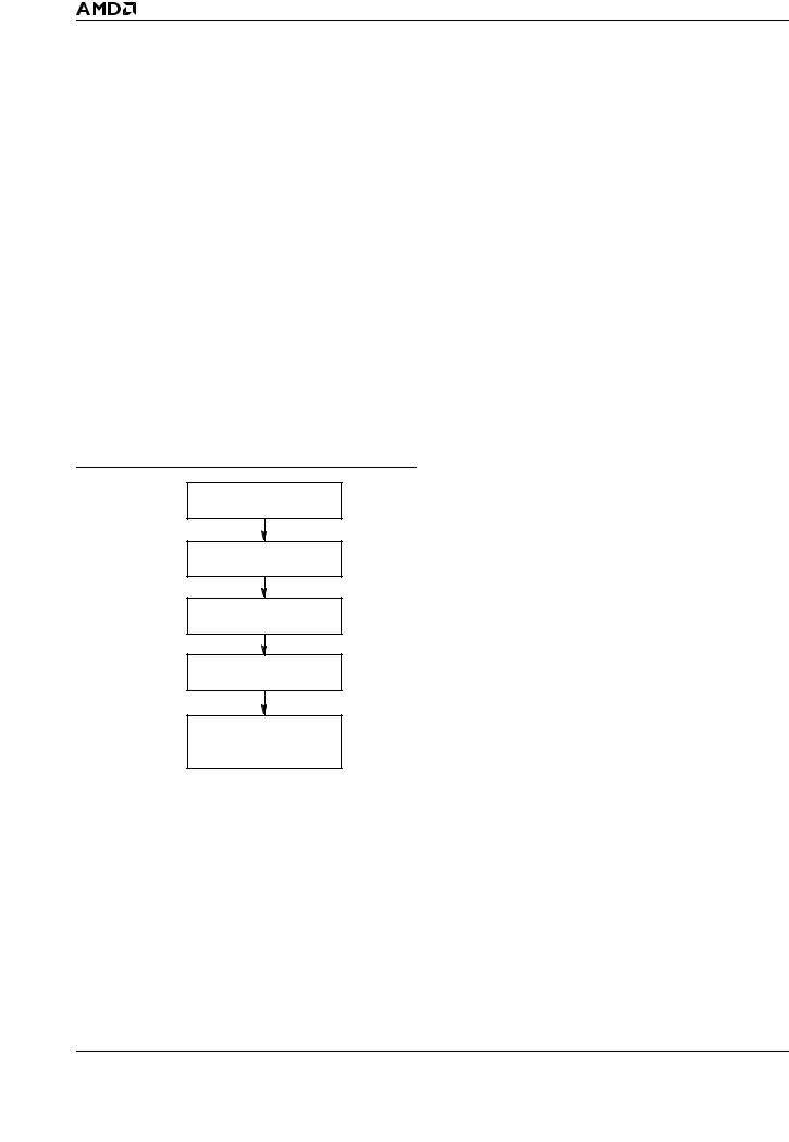
START
Write Program
Command Sequence
Data Poll
from System
Embedded Program algorithm in progress
Verify Data?
No
Yes
Increment Address |
No |
Last Address? |
|
|
Yes |
|
Programming |
|
Completed |
20818C-5
Note: See the appropriate Command Definitions table for program command sequence.
Figure 2. Program Operation
Chip Erase Command Sequence
Chip erase is a six-bus-cycle operation. The chip erase command sequence is initiated by writing two unlock cycles, followed by a set-up command. Two additional unlock write cycles are then followed by the chip erase
command, which in turn invokes the Embedded Erase algorithm. The device does not require the system to preprogram prior to erase. The Embedded Erase algorithm automatically preprograms and verifies the entire memory for an all zero data pattern prior to electrical erase. The system is not required to provide any controls or timings during these operations. The Command Definitions table shows the address and data requirements for the chip erase command sequence.
Any commands written to the chip during the Embedded Erase algorithm are ignored. On the Am29F002 only, note that a hardware reset during the sector erase operation immediately terminates the operation. The Sector Erase command sequence should be reinitiated once the device has returned to reading array data, to ensure data integrity.
The system can determine the status of the erase operation by using DQ7, DQ6, or DQ2. See “Write Operation Status” for information on these status bits. When the Embedded Erase algorithm is complete, the device returns to reading array data and addresses are no longer latched.
Figure 3 illustrates the algorithm for the erase operation. See the Erase/Program Operations tables in “AC Characteristics” for parameters, and to the Chip/Sector Erase Operation Timings for timing waveforms.
Sector Erase Command Sequence
Sector erase is a six bus cycle operation. The sector erase command sequence is initiated by writing two unlock cycles, followed by a set-up command. Two additional unlock write cycles are then followed by the address of the sector to be erased, and the sector erase command. The Command Definitions table shows the address and data requirements for the sector erase command sequence.
The device does not require the system to preprogram the memory prior to erase. The Embedded Erase algorithm automatically programs and verifies the sector for an all zero data pattern prior to electrical erase. The system is not required to provide any controls or timings during these operations.
After the command sequence is written, a sector erase time-out of 50 μs begins. During the time-out period, additional sector addresses and sector erase commands may be written. Loading the sector erase buffer may be done in any sequence, and the number of sectors may be from one sector to all sectors. The time between these additional cycles must be less than 50 μs, otherwise the last address and command might not be accepted, and erasure may begin. It is recommended that processor interrupts be disabled during this time to ensure all commands are accepted. The interrupts can be re-enabled after the last Sector Erase command is written. If the time between additional sector erase
12 |
Am29F002/Am29F002N |
 Loading...