


AMD Advanced Micro Devices AM29F400AT-90FIB, AM29F400AT-90FI, AM29F400AT-90FCB, AM29F400AT-90FC, AM29F400AT-90EIB Datasheet
...PRELIMINARY
Am29F400AT/Am29F400AB
4 Megabit (524,288 x 8-Bit/262,144 x 16-Bit) CMOS 5.0 Volt-only, Sector Erase Flash Memory
DISTINCTIVE CHARACTERISTICS
■5.0 V ± 10% for read and write operations
—Minimizes system level power requirements
■Compatible with JEDEC-standards
—Pinout and software compatible with
single-power-supply flash
—Superior inadvertent write protection
■Package options
—44-pin SO
—48-pin TSOP
■Minimum 100,000 write/erase cycles guaranteed
■High performance
—60 ns maximum access time
■Sector erase architecture
—One 16 Kbyte, two 8 Kbytes, one 32 Kbyte, and seven 64 Kbytes
—Any combination of sectors can be erased. Also supports full chip erase.
■Sector protection
—Hardware method that disables any combination of sectors from write or erase operations. Implemented using standard PROM programming equipment.
■Embedded Erase Algorithms
■Embedded Program Algorithms
—Automatically programs and verifies data at specified address
■Data Polling and Toggle Bit feature for detection of program or erase cycle completion
■Ready/Busy output (RY/BY)
—Hardware method for detection of program or erase cycle completion
■Erase Suspend/Resume
—Supports reading data from a sector not being erased
■Low power consumption
—20 mA typical active read current for Byte Mode
—28 mA typical active read current for Word Mode
—30 mA typical program/erase current
■Enhanced power management for standby mode
—1 A typical standby current
■Boot Code Sector Architecture
—T = Top sector
—B = Bottom sector
■Hardware RESET pin
—Resets internal state machine to the read mode
—Automatically preprograms and erases the chip or any sector
GENERAL DESCRIPTION
The Am29F400A is a 4 Mbit, 5.0 Volt-only Flash memory organized as 512 Kbytes of 8 bits each or 256 Kwords of 16 bits each. The 4 Mbits of data is divided into 11 sectors of one 16 Kbyte, two 8 Kbyte, one 32 Kbyte, and seven 64 Kbytes, for flexible erase capability. The 8 bits of data will appear on DQ0–DQ7 or 16 bits on DQ0–DQ15. The Am29F400A is offered in 44-pin SO and 48-pin TSOP packages. This device is designed to be programmed in-system with the standard system 5.0 Volt VCC supply. 12.0 Volt VPP is not required for program or erase operations. The device can also be reprogrammed in standard EPROM programmers.
The standard Am29F400A offers access times of 60 ns, 70 ns, 90 ns, 120 ns and 150 ns, allowing high speed microprocessors to operate without wait states. To eliminate bus contention the device has separate chip enable (CE), write enable (WE) and output enable (OE) controls.
The Am29F400A is entirely command set compatible with the JEDEC single-power-supply Flash standard. Commands are written to the command register using standard microprocessor write timings. Register contents serve as input to an internal state-machine which controls the erase and programming circuitry.
This document contains information on a product under development at Advanced Micro Devices. The information |
Publication# 20380 Rev: B Amendment/0 |
is intended to help you evaluate this product. AMD reserves the right to change or discontinue work on this proposed |
Issue Date: April 1997 |
product without notice. |
|
|
Flash only-V 0.5

P R E L I M I N A R Y
Write cycles also internally latch addresses and data needed for the programming and erase operations. Reading data out of the device is similar to reading from 12.0 Volt Flash or EPROM devices.
The Am29F400A is programmed by executing the program command sequence. This will invoke the Embedded Program Algorithm which is an internal algorithm that automatically times the program pulse widths and verifies proper cell margin. Erase is accomplished by executing the erase command sequence. This will invoke the Embedded Erase Algorithm which is an internal algorithm that automatically preprograms the array if it is not already programmed before executing the erase operation. During erase, the device automatically times the erase pulse widths and verifies proper cell margin.
This device also features a sector erase architecture. This allows for sectors of memory to be erased and reprogrammed without affecting the data contents of other sectors. A sector is typically erased and verified within 1.5 seconds. The Am29F400A is erased when shipped from the factory.
The Am29F400A device also features hardware sector protection. This feature will disable both program and erase operations in any combination of eleven sectors of memory.
AMD has implemented an Erase Suspend feature that enables the user to put erase on hold for any period of time to read data from a sector that was not being erased. Thus, true background erase can be achieved.
The device features single 5.0 Volt power supply operation for both read and write functions. Internally generated and regulated voltages are provided for the program and erase operations. A low VCC detector automatically inhibits write operations during power transitions. The end of program or erase is detected by the
RY/BY pin. Data Polling of DQ7, or by the Toggle Bit (DQ6). Once the end of a program or erase cycle has been completed, the device automatically resets to the read mode.
The Am29F400A also has a hardware RESET pin. When this pin is driven low, execution of any Embedded Program Algorithm or Embedded Erase Algorithm will be terminated. The internal state machine will then
be reset into the read mode. The RESET pin may be tied to the system reset circuitry. Therefore, if a system reset occurs during the Embedded Program Algorithm or Embedded Erase Algorithm, the device will be automatically reset to the read mode and will have erroneous data stored in the address locations being operated on. These locations will need rewriting after the Reset. Resetting the device will enable the system’s microprocessor to read the boot-up firmware from the Flash memory.
AMD’s Flash technology combines years of Flash memory manufacturing experience to produce the highest levels of quality, reliability and cost effectiveness. The Am29F400A memory electrically erases all b i t s w i t h i n a s e c t o r s i mu l t a n e o u s l y v i a Fowler-Nordhiem tunneling. The bytes/words are programmed one byte/word at a time using the EPROM programming mechanism of hot electron injection.
Flexible Sector-Erase Architecture
■One 16 Kbyte, two 8 Kbytes, one 32 Kbyte, and seven 64 Kbyte sectors
■Individual-sector or multiple-sector erase capability
■Sector protection is user definable
|
|
(x8) |
(x16) |
|
|
|
7FFFFh |
3FFFFh |
|
SA10 |
16 Kbyte |
|||
7BFFFh |
3DFFFh |
|||
|
||||
SA9 |
8 Kbyte |
|||
79FFFh |
3CFFFh |
|||
|
||||
SA8 |
8 Kbyte |
|||
77FFFh |
3BFFFh |
|||
|
||||
SA7 |
32 Kbyte |
|||
6FFFFh |
37FFFh |
|||
SA6 |
64 Kbyte |
|||
5FFFFh |
2FFFFh |
|||
|
||||
SA5 |
64 Kbyte |
|||
4FFFFh |
27FFFh |
|||
|
|
|||
SA4 |
64 Kbyte |
|||
3FFFFh |
1FFFFh |
|||
|
|
|||
SA3 |
64 Kbyte |
|||
2FFFFh |
17FFFh |
|||
|
|
|||
SA2 |
64 Kbyte |
|||
1FFFFh |
0FFFFh |
|||
|
|
|||
SA1 |
64 Kbyte |
|||
0FFFFh |
07FFFh |
|||
SA0 |
|
|||
64 Kbyte |
||||
00000h |
00000h |
|||
|
|
|||
|
|
|||
|
|
|
20380B-1 |
|
|
Am29F400AT Sector Architecture |
|
||
|
|
(x8) |
(x16) |
|
|
|
7FFFFh |
3FFFFh |
|
SA10 |
64 Kbyte |
|||
6BFFFh |
37FFFh |
|||
|
||||
SA9 |
64 Kbyte |
|||
5FFFFh |
2FFFFh |
|||
|
||||
SA8 |
64 Kbyte |
|||
4FFFFh |
27FFFh |
|||
SA7 |
64 Kbyte |
|||
3FFFFh |
1FFFFh |
|||
SA6 |
64 Kbyte |
|||
2FFFFh |
17FFFh |
|||
SA5 |
64 Kbyte |
|||
1FFFFh |
0FFFFh |
|||
|
|
|||
SA4 |
64 Kbyte |
|||
0FFFFh |
07FFFh |
|||
|
|
|||
SA3 |
32 Kbyte |
|||
07FFFh |
03FFFh |
|||
|
|
|||
SA2 |
8 Kbyte |
|||
05FFFh |
02FFFh |
|||
|
|
|||
SA1 |
8 Kbyte |
|||
03FFFh |
01FFFh |
|||
SA0 |
|
|||
16 Kbyte |
||||
00000h |
00000h |
|||
|
|
|||
|
|
|||
|
|
|
20380B-2 |
|
|
Am29F400AB Sector Architecture |
|||
2 |
Am29F400AT/Am29F400AB |

P R E L I M I N A R Y
PRODUCT SELECTOR GUIDE
|
|
|
|
|
|
|
Family Part No: |
|
|
Am29F400A |
|
|
|
|
|
|
|
|
|
||||||
|
Ordering Part No:VCC = 5.0 V ± 5% |
-65 |
|
|
|
|
||||||
|
|
|
|
|
|
|
VCC = 5.0 V ± 10% |
|
-70 |
-90 |
-120 |
-150 |
|
Max Access Time (ns) |
60 |
70 |
90 |
120 |
150 |
||||||
|
|
|
|
|
|
|
|
|
|
|
|
|
|
|
|
|
|
|
|
|
60 |
70 |
90 |
120 |
150 |
|
CE |
(E) Access (ns) |
||||||||||
|
|
|
|
|
|
|
|
|
|
|||
|
|
|
|
|
|
Access (ns) |
30 |
30 |
35 |
50 |
55 |
|
|
OE |
(G) |
||||||||||
|
|
|
|
|
|
|
|
|
|
|
|
|
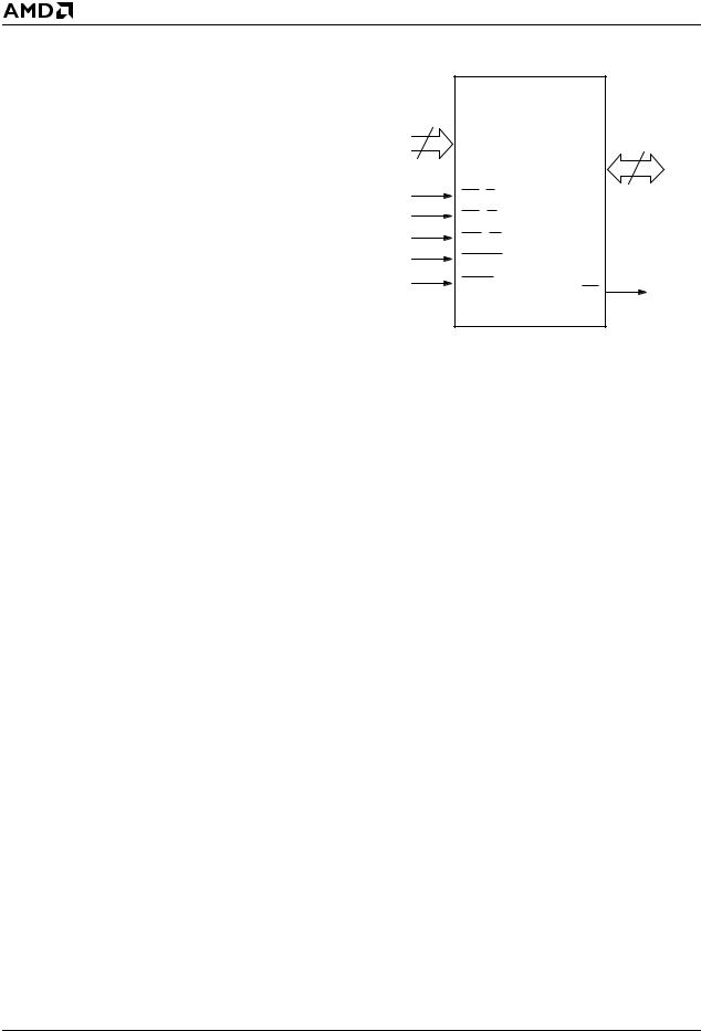
BLOCK DIAGRAM
|
|
|
|
|
|
DQ0–DQ15 |
|
RY/BY |
RY/BY |
|
|
|
|
VCC |
Buffer |
|
|
|
|
|
|
|
|
|
|
||
VSS |
|
Erase Voltage |
|
|
Input/Output |
|
|
|
|
Generator |
|
|
Buffers |
WE |
State |
|
|
|
|
|
Control |
|
|
|
|
|
|
BYTE |
|
|
|
|
|
|
|
|
|
|
|
|
|
RESET |
Command |
PGM Voltage |
|
|
|
|
|
Register |
|
|
|
|
|
|
|
Generator |
Chip Enable |
|
Data |
|
|
|
|
STB |
|||
CE |
|
|
Output Enable |
Latch |
||
|
|
|
||||
OE |
|
|
|
Logic |
|
|
|
|
|
STB |
Y-Decoder |
|
Y-Gating |
|
|
|
|
|
|
|
|
VCC Detector |
Timer |
Latch |
|
|
|
|
|
|
Address |
X-Decoder |
|
Cell Matrix |
|
|
|
|
|
||
A0-A17 |
|
|
|
|
|
|
A-1 |
|
|
|
|
|
|
20380B-3
Flash only-V 0.5
Am29F400AT/Am29F400AB |
3 |

P R E L I M I N A R Y
CONNECTION DIAGRAMS
SO
|
|
|
|
|
|
44 |
|
|
|
|
|
|
|
NC |
|
1 |
|
RESET |
|||||||
|
|
|
|
|
|
|
|
|
|
|
|
|
RY/BY |
|
|
|
2 |
43 |
|
|
WE |
||||
A17 |
|
3 |
42 |
|
|
A8 |
||||||
|
|
|||||||||||
|
A7 |
|
4 |
41 |
|
|
A9 |
|||||
|
|
|||||||||||
|
A6 |
|
5 |
40 |
|
|
A10 |
|||||
|
|
|
||||||||||
|
A5 |
|
6 |
39 |
|
|
A11 |
|||||
|
|
|
||||||||||
|
A4 |
|
7 |
38 |
|
|
A12 |
|||||
|
|
|||||||||||
|
A3 |
|
8 |
37 |
|
|
A13 |
|||||
|
|
|||||||||||
|
A2 |
|
9 |
36 |
|
|
A14 |
|||||
|
|
|
||||||||||
|
A1 |
|
10 |
35 |
|
|
A15 |
|||||
|
|
|
||||||||||
|
A0 |
|
11 |
34 |
|
|
A16 |
|||||
|
|
|
||||||||||
|
|
|
|
|
12 |
33 |
|
|
|
|
||
|
CE |
|
|
|
|
|
BYTE |
|||||
VSS |
|
13 |
32 |
|
|
VSS |
||||||
|
|
|||||||||||
|
|
|
|
14 |
31 |
|
|
DQ15/A-1 |
||||
|
OE |
|
|
|||||||||
DQ0 |
|
15 |
30 |
|
|
DQ7 |
||||||
|
|
|||||||||||
DQ8 |
|
16 |
29 |
|
|
DQ14 |
||||||
|
|
|
||||||||||
DQ1 |
|
17 |
28 |
|
|
DQ6 |
||||||
|
|
|
||||||||||
DQ9 |
|
18 |
27 |
|
|
DQ13 |
||||||
|
|
|
||||||||||
DQ2 |
|
19 |
26 |
|
|
DQ5 |
||||||
|
|
|||||||||||
DQ10 |
|
20 |
25 |
|
|
DQ12 |
||||||
|
|
|||||||||||
DQ3 |
|
21 |
24 |
|
|
DQ4 |
||||||
|
|
|
||||||||||
DQ11 |
|
22 |
23 |
|
|
VCC |
||||||
|
|
|||||||||||
|
|
|
|
|
|
|
|
|
|
|
|
|
20380B-4
4 |
Am29F400AT/Am29F400AB |

P R E L I M I N A R Y
CONNECTION DIAGRAMS
A15  1
1 
A14  2
2
A13  3
3
A12  4
4
A11  5
5
A10  6
6
A9  7
7
A8  8
8
NC  9
9
NC  10
10
WE  11
11
RESET  12
12
NC  13
13
NC  14
14
RY/BY  15
15
NC  16
16
A17  17
17
A7  18
18
A6  19
19
A5  20
20
A4  21
21
A3  22
22
A2  23
23
A1  24
24
Standard TSOP
A16  1
1
BYTE  2
2
VSS  3
3
DQ15/A-1  4
4
DQ7  5
5
DQ14  6
6
DQ6  7
7
DQ13  8
8
DQ5  9
9
DQ12  10
10
DQ4  11
11
VCC  12
12
DQ11  13
13
DQ3  14
14
DQ10  15
15
DQ2  16
16
DQ9  17
17
DQ1  18
18
DQ8  19
19
DQ0  20
20
OE  21
21
VSS  22
22
CE  23
23
A0  24
24
Reverse TSOP
48  A16
A16
47  BYTE
BYTE
46  VSS
VSS
45  DQ15/A-1
44  DQ7
DQ7
43  DQ14
DQ14
42  DQ6
DQ6
41  DQ13
DQ13
40  DQ5
DQ5
39  DQ12
DQ12
38  DQ4
DQ4
37  VCC
VCC
36  DQ11
DQ11
35  DQ3
DQ3
34  DQ10
DQ10
33  DQ2
DQ2
32  DQ9
DQ9
31  DQ1
DQ1
30  DQ8
DQ8
29  DQ0
DQ0
28  OE
OE
27  VSS
VSS
26  CE
CE
25  A0
A0
20380B-5
48  A15
A15
47  A14
A14
46  A13
A13
45  A12
A12
44  A11
A11
43  A10
A10
42  A9
A9
41  A8
A8
40  NC
NC
39  NC
NC
38  WE
WE
37  RESET
RESET
36  NC
NC
35  NC
NC
34  RY/BY
RY/BY
33  NC
NC
32  A17
A17
31  A7
A7
30  A6
A6
29  A5
A5
28  A4
A4
27  A3
A3
26  A2
A2
25  A1
A1
20380B-6
Flash only-V 0.5
Am29F400AT/Am29F400AB |
5 |
P R E L I M I N A R Y
PIN CONFIGURATION
A1, A0–A17 = |
18 Addresses |
|||||||||
|
|
|
|
|
|
|
= |
Selects 8-bit or 16-bit mode |
||
BYTE |
||||||||||
|
|
|
|
|
|
= |
Chip Enable |
|||
CE |
||||||||||
DQ0–DQ15 = |
16 Data Inputs/Outputs |
|||||||||
NC |
= |
Pin Not Connected Internally |
||||||||
|
|
|
|
|
= |
Output Enable |
||||
OE |
||||||||||
|
|
|
|
= |
Hardware Reset Pin, Active Low |
|||||
RESET |
||||||||||
|
|
|
= |
|
|
Output |
||||
RY/BY |
Ready/Busy |
|||||||||
VSS |
= |
+5.0 Volt Single-Power Supply |
||||||||
|
|
|
|
|
|
|
|
(±10% for -90, -120, -150) or (±5% for -75) |
||
VSS |
= |
Device Ground |
||||||||
|
|
= |
Write Enable |
|||||||
WE |
||||||||||
LOGIC SYMBOL
 A-1 18
A0–A17 |
16 or 8 |
DQ0–DQ15
CE (E)
OE (G)
WE (W)
RESET
BYTE
RY/BY
20380B-7
6 |
Am29F400AT/Am29F400AB |
P R E L I M I N A R Y
ORDERING INFORMATION
Standard Products
AMD standard products are available in several packages and operating ranges. The order number (Valid Combination) is formed by a combination of the following:
AM29F400A T |
-65 |
E |
C |
B |
|
|
|
|
|
|
|
OPTIONAL PROCESSING
Blank = Standard Processing
B = Burn-In
TEMPERATURE RANGE
C = Commercial (0°C to +70°C)
I = Industrial (-40°C to +85°C)
PACKAGE TYPE
E = 48-Pin Thin Small Outline Package
(TSOP) Standard Pinout (TS 048)
F = 48-Pin Thin Small Outline Package
(TSOP) Reverse Pinout (TSR048)
S = 44-Pin Small Outline Package (SO 044)
SPEED OPTION
See Product Selector Guide and
Valid Combinations
BOOT CODE SECTOR ARCHITECTURE
T = Top sector
B = Bottom sector
DEVICE NUMBER/DESCRIPTION
Am29F400A
4 Megabit (512K x 8-Bit/256K x 16-Bit) CMOS Flash Memory
5.0 Volt-only Program and Erase
Flash only-V 0.5
Valid Combinations
AM29F400AT/B-65 |
EC, EI, FC, FI, SC, SI |
|
|
|
|
AM29F400AT/B-70 |
|
|
|
EC, EI, EE, EEB, |
|
AM29F400AT/B-90 |
||
|
FC, FI, FE, FEB, |
|
AM29F400AT/B-120 |
||
SC, SI, SE, SEB |
||
|
|
|
AM29F400AT/B-150 |
|
|
|
|
Valid Combinations
Valid Combinations list configurations planned to be supported in volume for this device. Consult the local AMD sales office to confirm availability of specific valid combinations and to check on newly released combinations.
Am29F400AT/Am29F400AB |
7 |

P R E L I M I N A R Y
Table 1. Am29F400A User Bus Operations (BYTE = VIH)
|
|
|
|
|
|
|
|
|
|
|
|
|
|
|
|
|
|
|
Operation |
|
CE |
|
|
OE |
|
WE |
A0 |
A1 |
A6 |
A9 |
DQ0–DQ15 |
|
RESET |
||||
|
|
|
|
|
|
|
|
|
|
|
|
|
|
|
|
|||
Autoselect, AMD Manuf. Code (Note 1) |
|
L |
|
|
L |
|
H |
L |
L |
L |
VID |
Code |
|
H |
||||
Autoselect Device Code (Note 1) |
|
L |
|
|
L |
|
H |
H |
L |
L |
VID |
Code |
|
H |
||||
Read |
|
L |
|
|
L |
|
H |
A0 |
A1 |
A6 |
A9 |
DOUT |
|
H |
||||
Standby |
|
H |
|
|
X |
|
X |
X |
X |
X |
X |
HIGH Z |
|
H |
||||
|
|
|
|
|
|
|
|
|
|
|
|
|
|
|
|
|||
Output Disable |
|
L |
|
|
H |
|
H |
X |
X |
X |
X |
HIGH Z |
|
H |
||||
|
|
|
|
|
|
|
|
|
|
|
|
|
|
|
|
|||
Write |
|
L |
|
|
H |
|
L |
A0 |
A1 |
A6 |
A9 |
DIN |
|
H |
||||
Verify Sector Protect (Note 2) |
|
L |
|
|
L |
|
H |
L |
H |
L |
VID |
Code |
|
H |
||||
Temporary Sector Unprotect |
|
X |
|
|
X |
|
X |
X |
X |
X |
X |
X |
|
VID |
||||
Hardware Reset |
|
X |
|
|
X |
|
X |
X |
X |
X |
X |
HIGH Z |
|
L |
||||
|
|
|
|
|
|
|
|
|
|
|
|
|
|
|
|
|
|
|
|
|
|
|
|
|
|
|
|
|
|
|
|
|
|
|
|
|
|
Table 2. Am29F400A User Bus Operations (BYTE = VIL)
|
|
|
|
|
|
|
|
|
|
|
|
|
|
|
|
|
|
|
Operation |
|
CE |
|
|
OE |
|
WE |
A0 |
A1 |
A6 |
A9 |
DQ0–DQ7 |
DQ8–DQ15 |
|
RESET |
|||
|
|
|
|
|
|
|
|
|
|
|
|
|
|
|
|
|
|
|
Autoselect, AMD Manuf. Code |
|
L |
|
|
L |
|
H |
L |
L |
L |
VID |
Code |
HIGH Z |
|
H |
|||
(Note 1) |
|
|
|
|
|
|||||||||||||
Autoselect Device Code (Note 1) |
|
L |
|
|
L |
|
H |
H |
L |
L |
VID |
Code |
HIGH Z |
|
H |
|||
Read |
|
L |
|
|
L |
|
H |
A0 |
A1 |
A6 |
A9 |
DOUT |
HIGH Z |
|
H |
|||
Standby |
|
H |
|
|
X |
|
X |
X |
X |
X |
X |
HIGH Z |
HIGH Z |
|
H |
|||
|
|
|
|
|
|
|
|
|
|
|
|
|
|
|
|
|||
Output Disable |
|
L |
|
|
H |
|
H |
X |
X |
X |
X |
HIGH Z |
HIGH Z |
|
H |
|||
|
|
|
|
|
|
|
|
|
|
|
|
|
|
|
|
|||
Write |
|
L |
|
|
H |
|
L |
A0 |
A1 |
A6 |
A9 |
DIN |
HIGH Z |
|
H |
|||
Verify Sector Protect (Note 2) |
|
L |
|
|
L |
|
H |
L |
H |
L |
VID |
Code |
HIGH Z |
|
H |
|||
Temporary Sector Unprotect |
|
X |
|
|
X |
|
X |
X |
X |
X |
X |
X |
HIGH Z |
|
VID |
|||
Hardware Reset |
|
X |
|
|
X |
|
X |
X |
X |
X |
X |
HIGH Z |
HIGH Z |
|
L |
|||
|
|
|
|
|
|
|
|
|
|
|
|
|
|
|
|
|
|
|
Legend:
L = logic 0, H = logic 1, X = Don’t Care. See Characteristics for voltage levels.
Notes:
1.Manufacturer and device codes may also be accessed via a command register write sequence. Refer to Table 4.
2.Refer to the section on Sector Protection.
Read Mode
The Am29F400A has two control functions which must
be satisfied in order to obtain data at the outputs. CEis the power control and should be used for device selection. OE is the output control and should be used to gate data to the output pins if a device is selected.
Address access time (tACC) is equal to the delay from stable addresses to valid output data. The chip enable access time (tCE) is the delay from stable addresses
and stable CE to valid data at the output pins. The output enable access time is the delay from the falling edge of OE to valid data at the output pins (as-
suming the addresses have been stable for at least tACC-tOE time).
Standby Mode
There are two ways to implement the standby mode on the Am29F400A device, both using the CE pin.
A CMOS standby mode is achieved with the CE input held at VCC ± 0.5 V. Under this condition the current is typically reduced to less than 5 A. A TTL standby mode is achieved with the CE pin held at VIH. Under this condition the current is typically reduced to 1 mA.
In the standby mode the outputs are in the high impedance state, independent of the OE input.
8 |
Am29F400AT/Am29F400AB |

P R E L I M I N A R Y
Output Disable
With the OE input at a logic high level (VIH), output from the device is disabled. This will cause the output pins to be in a high impedance state.
Autoselect
The autoselect mode allows the reading of a binary code from the device and will identify its manufacturer and type. This mode is intended for use by programming equipment for the purpose of automatically matching the device to be programmed with its corresponding programming algorithm. This mode is functional over the entire temperature range of the device.
To activate this mode, the programming equipment must force VID (11.5 V to 12.5 V) on address pin A9. Two identifier bytes may then be sequenced from the device outputs by toggling address A0 from VIL to VIH. All addresses are don’t cares except A0, A1, and A6 (see Table 3).
The manufacturer and device codes may also be read via the command register, for instances when the
Am29F400A is erased or programmed in a system without access to high voltage on the A9 pin. The command sequence is illustrated in Table 4 (see Autoselect Command Sequence).
Byte 0 (A0 = VIL) represents the manufacturer’s code (AMD=01H) and byte 1 (A0 = VIH) the device identifier code (Am29F400AT = 23H and Am29F400AB = ABH for x8 mode; Am29F400AT = 2223H and Am29F400AB = 22ABH for x16 mode). These two bytes/words are given in the table below. All identifiers for manufacturer and device will exhibit odd parity with DQ7 defined as the parity bit. In order to read the proper device codes when executing the Autoselect, A1 must be VIL (see Tables 3 and 4).
The autoselect mode also facilitates the determination of sector protection in the system. By performing a read operation at the address location XX02H with the higher order address bits A12–A17 set to the desired sector address, the device will return 01H for a protected sector and 00H for a non-protected sector.
Table 3. Am29F400A Sector Protection Verify Autoselect Codes
Type |
A12-A17 |
A6 |
A1 |
A0 |
Code (HEX) |
|||
|
|
|
|
|
|
|||
Manufacturer Code-AMD |
X |
VIL |
VIL |
VIL |
01H |
|||
|
Am29F400AT |
Byte |
X |
VIL |
VIL |
VIH |
23H |
|
|
|
|
||||||
Am29F400A Device |
Word |
2223H |
||||||
|
|
|
|
|
||||
|
|
|
|
|
|
|
||
Am29F400AB |
Byte |
X |
VIL |
VIL |
VIH |
ABH |
||
|
||||||||
|
|
|
||||||
|
Word |
22ABH |
||||||
|
|
|
|
|
|
|||
|
|
|
|
|
|
|
|
|
Sector Protection |
Sector |
VIL |
VIH |
VIL |
01H* |
|||
Address |
||||||||
*Outputs 01H at protected sector addresses
Table 4. Expanded Autoselect Code Table
|
|
Code |
DQ |
DQ |
DQ |
DQ |
DQ |
DQ |
DQ |
DQ |
DQ |
DQ |
DQ |
DQ |
DQ |
DQ |
DQ |
DQ |
Type |
|
15 |
14 |
13 |
12 |
11 |
10 |
9 |
8 |
7 |
6 |
5 |
4 |
3 |
2 |
1 |
0 |
|
|
|
|||||||||||||||||
|
|
|
|
|
|
|
|
|
|
|
|
|
|
|
|
|
|
|
Manufacturer Code-AMD |
01H |
0 |
0 |
0 |
0 |
0 |
0 |
0 |
0 |
0 |
0 |
0 |
0 |
0 |
0 |
0 |
1 |
|
|
|
|
|
|
|
|
|
|
|
|
|
|
|
|
|
|
|
|
|
Am29F400AT(B) |
23H |
A-1 |
HI-Z |
HI-Z |
HI-Z |
HI-Z |
HI-Z |
HI-Z |
HI-Z |
0 |
0 |
1 |
0 |
0 |
0 |
1 |
1 |
Am29F400A |
(W) |
2223H |
0 |
0 |
1 |
0 |
0 |
0 |
1 |
0 |
0 |
0 |
1 |
0 |
0 |
0 |
1 |
1 |
|
|
|
|
|
|
|
|
|
|
|
|
|
|
|
|
|
|
|
Device |
Am29F400AB(B) |
ABH |
A-1 |
HI-Z |
HI-Z |
HI-Z |
HI-Z |
HI-Z |
HI-Z |
HI-Z |
1 |
0 |
1 |
0 |
1 |
0 |
1 |
1 |
|
||||||||||||||||||
|
(W) |
22ABH |
0 |
0 |
1 |
0 |
0 |
0 |
1 |
0 |
1 |
0 |
1 |
0 |
1 |
0 |
1 |
1 |
|
|
|
|
|
|
|
|
|
|
|
|
|
|
|
|
|
|
|
Sector Protection |
01H |
0 |
0 |
0 |
0 |
0 |
0 |
0 |
0 |
0 |
0 |
0 |
0 |
0 |
0 |
0 |
1 |
|
|
|
|
|
|
|
|
|
|
|
|
|
|
|
|
|
|
|
|
B) - Byte mode
(W) - Word mode
Flash only-V 0.5
Am29F400AT/Am29F400AB |
9 |

P R E L I M I N A R Y
Table 5. Sector Address Tables (Am29F400AT)
|
|
|
|
|
|
|
(x8) Address |
(x16) Address |
|
A17 |
A16 |
A15 |
A14 |
A13 |
A12 |
Range |
Range |
|
|
|
|
|
|
|
|
|
SA0 |
0 |
0 |
0 |
X |
X |
X |
00000h-0FFFFh |
00000h-07FFFh |
|
|
|
|
|
|
|
|
|
SA1 |
0 |
0 |
1 |
X |
X |
X |
10000h-1FFFFh |
08000h-0FFFFh |
|
|
|
|
|
|
|
|
|
SA2 |
0 |
1 |
0 |
X |
X |
X |
20000h-2FFFFh |
10000h-17FFFh |
|
|
|
|
|
|
|
|
|
SA3 |
0 |
1 |
1 |
X |
X |
X |
30000h-3FFFFh |
18000h-1FFFFh |
|
|
|
|
|
|
|
|
|
SA4 |
1 |
0 |
0 |
X |
X |
X |
40000h-4FFFFh |
20000h-27FFFh |
|
|
|
|
|
|
|
|
|
SA5 |
1 |
0 |
1 |
X |
X |
X |
50000h-5FFFFh |
28000h-2FFFFh |
|
|
|
|
|
|
|
|
|
SA6 |
1 |
1 |
0 |
X |
X |
X |
60000h-6FFFFh |
30000h-37FFFh |
|
|
|
|
|
|
|
|
|
SA7 |
1 |
1 |
1 |
0 |
X |
X |
70000h-77FFFh |
38000h-3BFFFh |
|
|
|
|
|
|
|
|
|
SA8 |
1 |
1 |
1 |
1 |
0 |
0 |
78000h-79FFFh |
3C000h-3CFFFh |
|
|
|
|
|
|
|
|
|
SA9 |
1 |
1 |
1 |
1 |
0 |
1 |
7A000h-7BFFFh |
3D000h-3DFFFh |
|
|
|
|
|
|
|
|
|
SA10 |
1 |
1 |
1 |
1 |
1 |
X |
7C000h-7FFFFh |
3E000h-3FFFFh |
|
|
|
|
|
|
|
|
|
Table 6. Sector Address Tables (Am29F400AB)
|
|
|
|
|
|
|
(x8) Address |
(x16) Address |
|
A17 |
A16 |
A15 |
A14 |
A13 |
A12 |
Range |
Range |
|
|
|
|
|
|
|
|
|
SA0 |
0 |
0 |
0 |
0 |
0 |
X |
00000h-03FFFh |
00000h-01FFFh |
|
|
|
|
|
|
|
|
|
SA1 |
0 |
0 |
0 |
0 |
1 |
0 |
04000h-05FFFh |
02000h-02FFFh |
|
|
|
|
|
|
|
|
|
SA2 |
0 |
0 |
0 |
0 |
1 |
1 |
06000h-07FFFh |
03000h-03FFFh |
|
|
|
|
|
|
|
|
|
SA3 |
0 |
0 |
0 |
1 |
X |
X |
08000h-0FFFFh |
04000h-07FFFh |
|
|
|
|
|
|
|
|
|
SA4 |
0 |
0 |
1 |
X |
X |
X |
10000h-1FFFFh |
08000h-0FFFFh |
|
|
|
|
|
|
|
|
|
SA5 |
0 |
1 |
0 |
X |
X |
X |
20000h-2FFFFh |
10000h-17FFFh |
|
|
|
|
|
|
|
|
|
SA6 |
0 |
1 |
1 |
X |
X |
X |
30000h-3FFFFh |
18000h-1FFFFh |
|
|
|
|
|
|
|
|
|
SA7 |
1 |
0 |
0 |
X |
X |
X |
40000h-4FFFFh |
20000h-27FFFh |
|
|
|
|
|
|
|
|
|
SA8 |
1 |
0 |
1 |
X |
X |
X |
50000h-5FFFFh |
28000h-2FFFFh |
|
|
|
|
|
|
|
|
|
SA9 |
1 |
1 |
0 |
X |
X |
X |
60000h-6FFFFh |
30000h-37FFFh |
|
|
|
|
|
|
|
|
|
SA10 |
1 |
1 |
1 |
X |
X |
X |
70000h-7FFFFh |
38000h-3FFFFh |
|
|
|
|
|
|
|
|
|
Write
Device erasure and programming are accomplished via the command register.The contents of the register serve as inputs to the internal state machine. The state machine outputs dictate the function of the device.
The command register itself does not occupy any addressable memory location. The register is a latch used to store the commands, along with the address and data information needed to execute the command. The command register is written to by bringing WE to VIL, while
CE is at VIL and OE is at VIH. Addresses are latched on
the falling edge of WE or CE, whichever happens later; while data is latched on the rising edge of WE or CE, whichever happens first. Standard microprocessor write timings are used.
Refer to AC Write Characteristics and the Erase/Programming Waveforms for specific timing parameters.
Sector Protection
The Am29F400A features hardware sector protection. This feature will disable both program and erase operations in any combination of ten sectors of memory. The sector protect feature is enabled using programming equipment at the user’s site. The device is shipped with all sectors unprotected. Alternatively, AMD may program and protect sectors in the factory prior to shipping the device (AMD’s ExpressFlash Service).
10 |
Am29F400AT/Am29F400AB |
P R E L I M I N A R Y
It is possible to determine if a sector is protected in the system by writing an Autoselect command. Performing a read operation at the address location XX02H, where the higher order address bits A12–A17 is the desired sector address, will produce a logical “1” at DQ0 for a protected sector. See Table 3 for Autoselect codes.
Temporary Sector Unprotect
This feature allows temporary unprotection of previously protected sectors of the Am29F400A device in order to change data in-system. The Sector Unprotect mode is activated by setting the RESET pin to high voltage (12V). During this mode, formerly protected sectors can be programmed or erased by selecting the sector addresses. Once the 12 V is taken away from
the RESET pin, all the previously protected sectors will be protected again. Refer to Figures 16 and 17.
Command Definitions
Device operations are selected by writing specific address and data sequences into the command register.
Writing incorrect address and data values or writing them in the improper sequence will reset the device to the read mode. Table 7 defines the valid register command sequences. Note that the Erase Suspend (B0H) and Erase Resume (30H) commands are valid only while the Sector Erase operation is in progress. Moreover, both Reset/Read commands are functionally equivalent, resetting the device to the read mode.
Flash only-V 0.5
Am29F400AT/Am29F400AB |
11 |
 Loading...