


 Loading...
AMD Advanced Micro Devices AM28F512A-90PIB, AM28F512A-90PI, AM28F512A-90PEB, AM28F512A-90PE, AM28F512A-90PCB Datasheet
...FINAL
Am28F512A
512 Kilobit (64 K x 8-Bit)
CMOS 12.0 Volt, Bulk Erase Flash Memory with Embedded Algorithms
DISTINCTIVE CHARACTERISTICS
■High performance
—70 ns maximum access time
■CMOS low power consumption
—30 mA maximum active current
—100 µA maximum standby current
—No data retention power consumption
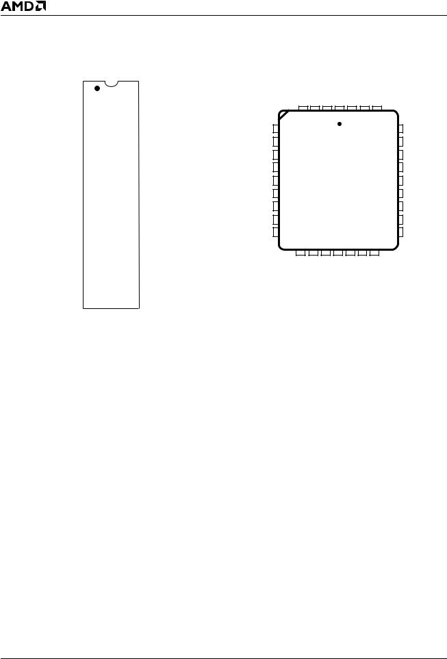
■Compatible with JEDEC-standard byte-wide 32-Pin EPROM pinouts
—32-pin PDIP
—32-pin PLCC
—32-pin TSOP
■100,000 write/erase cycles minimum
■Write and erase voltage 12.0 V −5%
■Latch-up protected to 100 mA from -1 V to VCC +1 V
■Embedded Erase Electrical Bulk Chip-Erase
—Two seconds typical chip-erase including pre-programming
■Embedded Program
—4 µs typical byte-program including time-out
—One second typical chip program
■Command register architecture for microprocessor/microcontroller compatible write interface
■On-chip address and data latches
■Advanced CMOS flash memory technology
—Low cost single transistor memory cell
■Embedded algorithms for completely self-timed write/erase operations
GENERAL DESCRIPTION
The Am28F512A is a 512 Kbit Flash memory organized as 64 Kbytes of 8 bits each. AMD’s Flash memories offer the most cost-effective and reliable read/write nonvolatile random access memory. The Am28F512A is packaged in 32-pin PDIP, PLCC, and TSOP versions. It is designed to be reprogrammed and erased in-sys- tem or in standard EPROM programmers. The Am28F512A is erased when shipped from the factory.
The standard Am28F512A offers access times as fast as 70 ns, allowing operation of high-speed microprocessors without wait states. To eliminate bus contention, the Am28F512A has separate chip enable (CE#) and output enable (OE#) controls.
AMD’s Flash memories augment EPROM functionality with in-circuit electrical erasure and programming. The Am28F512A uses a command register to manage this functionality, while maintaining a JEDEC Flash standard 32-pin pinout. The command register allows for 100% TTL level control inputs and fixed power supply levels during erase and programming.
AMD’s Flash technology reliably stores memory contents even after 100,000 erase and program cycles. The AMD cell is designed to optimize the erase and
programming mechanisms. In addition, the combination of advanced tunnel oxide processing and low internal electric fields for erase and programming operations produces reliable cycling. The Am28F512A uses a 12.0V± 5% VPP high voltage input to perform the erase and programming functions.
The highest degree of latch-up protection is achieved with AMD’s proprietary non-epi process. Latch-up protection is provided for stresses up to 100 milliamps on address and data pins from –1 V to VCC +1 V.
Embedded Program
The Am28F512A is byte programmable using the Embedded Programming algorithm. The Embedded Programming algorithm does not require the system to time-out or verify the data programmed. The typical r oo m te m pe ra t ur e pr ogra m m ing tim e o f th e Am28F512A is one second.
Embedded Erase
The entire chip is bulk erased using the Embedded Erase algorithm. The Embedded Erase algorithm automatically programs the entire array prior to electrical erase. The timing and verification of electrical erase are
Publication# 18880 Rev: C Amendment/+2
Issue Date: April 1998

controlled internal to the device. Typical erasure at room temperature is accomplished in two seconds, including programming.
AMD’s Am28F512A is entirely pin and software compatible with AMD Am28F020A, Am28F010A, and Am28F256A Flash memories.
Comparing Embedded Algorithms with Flasherase and Flashrite Algorithms
|
Am28F512A with |
Am28F512 using AMD Flashrite |
|
Embedded Algorithms |
and Flasherase Algorithms |
|
|
|
Embedded |
AMD’s Embedded Programming algorithm |
The Flashrite Programming algorithm requires the |
Programming |
requires the user to only write a program |
user to write a program set-up command, a program |
Algorithm vs. |
set-up command and a program command |
command, (program data and address), and a |
Flashrite |
(program data and address). The device |
program verify command, followed by a read and |
Programming |
automatically times the programming |
compare operation. The user is required to time the |
Algorithm |
pulse width, verifies the programming, and |
programming pulse width in order to issue the |
|
counts the number of sequences. A status |
program verify command. An integrated stop timer |
|
bit, Data# Polling, provides the user with |
prevents any possibility of overprogramming. |
|
the programming operation status. |
Upon completion of this sequence, the data is read |
|
|
|
|
|
back from the device and compared by the user with |
|
|
the data intended to be written; if there is not a |
|
|
match, the sequence is repeated until there is a |
|
|
match or the sequence has been repeated 25 times. |
|
|
|
Embedded Erase |
AMD’s Embedded Erase algorithm |
The Flasherase Erase algorithm requires the device |
Algorithm vs. |
requires the user to only write an erase set- |
to be completely programmed prior to executing an |
Flasherase Erase |
up command and erase command. The |
erase command. |
Algorithm |
device automatically pre-programs and |
To invoke the erase operation, the user writes an |
|
verifies the entire array. The device then |
|
|
erase set-up command, an erase command, and an |
|
|
automatically times the erase pulse width, |
|
|
erase verify command. The user is required to time |
|
|
verifies the erase operation, and counts |
|
|
the erase pulse width in order to issue the erase |
|
|
the number of sequences. A status bit, |
|
|
verify command. An integrated stop timer prevents |
|
|
Data# Polling, provides the user with the |
|
|
any possibility of overerasure. |
|
|
erase operation status. |
|
|
Upon completion of this sequence, the data is read |
|
|
|
|
|
|
back from the device and compared by the user with |
|
|
erased data. If there is not a match, the sequence is |
|
|
repeated until there is a match or the sequence has |
|
|
been repeated 1,000 times. |
|
|
|
Commands are written to the command register using standard microprocessor write timings. Register contents serve as inputs to an internal state-machine which controls the erase and programming circuitry. During write cycles, the command register internally latches address and data needed for the programming and erase operations. For system design simplification, the Am28F512A is designed to support either WE# or CE controlled writes. During a system write cycle, addresses are latched on the falling edge of WE# or CE# whichever occurs last. Data is latched on the rising edge of WE# or CE# whichever occurs first.
To simplify the following discussion, the WE# pin is used as the write cycle control pin throughout the rest of this text. All setup and hold times are with respect to the WE# signal.
AMD’s Flash technology combines years of EPROM and EEPROM experience to produce the highest levels of quality, reliability, and cost effectiveness. The Am28F512A electrically erases all bits simultaneously using Fowler-Nordheim tunneling. The bytes are programmed one byte at a time using the EPROM programming mechanism of hot electron injection.
2 |
Am28F512A |

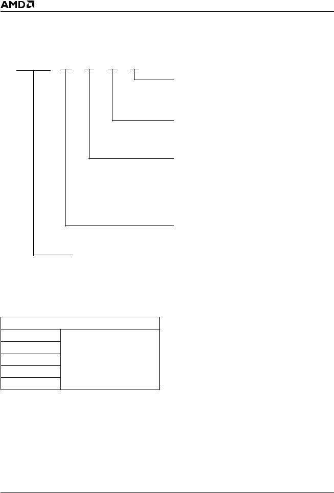
BLOCK DIAGRAM
DQ0–DQ7
VCC
VSS
VPP |
|
|
Erase Voltage |
Input/Output |
|
|
|
Switch |
|
Buffers |
|
|
|
|
|
||
|
State |
|
To Array |
|
|
WE# |
|
|
|
|
|
Control |
|
|
|
|
|
|
|
|
|
|
|
|
Command |
|
|
|
|
|
Register |
Program |
|
|
|
|
|
Voltage Switch |
Chip Enable |
Data |
|
|
|
|
|
||
CE# |
|
|
|
Output Enable |
Latch |
OE# |
|
|
|
Logic |
|
|
Embedded |
|
|
|
|
|
Algorithms |
|
|
|
|
|
|
|
|
Y-Decoder |
Y-Gating |
Low VCC |
Program/Erase |
Latch |
|
|
|
|
Pulse Timer |
|
|
||
Detector |
|
|
|
|
|
|
|
|
Address |
X-Decoder |
524,288 |
|
|
|
Bit Cell Matrix |
||
A0–A15 |
|
|
|
|
|
|
|
|
|
|
|
|
|
|
|
|
|
18880C-1 |
|
|
|
|
|
|
|
PRODUCT SELECTOR GUIDE |
|
|
|
|
|
|
|
|
|
|
|
|
|
Family Part Number |
|
|
Am28F512A |
|
|
|
|
|
|
|
|
|
|
Speed Options (VCC = 5.0 V ±10%) |
-70 |
-90 |
-120 |
|
-150 |
-200 |
|
|
|
|
|
|
|
Max Access Time (ns) |
70 |
90 |
120 |
|
150 |
200 |
|
|
|
|
|
|
|
CE# (E#) Access (ns) |
70 |
90 |
120 |
|
150 |
200 |
|
|
|
|
|
|
|
OE# (G#) Access (ns) |
35 |
35 |
50 |
|
55 |
55 |
|
|
|
|
|
|
|
Am28F512A |
3 |
CONNECTION DIAGRAMS
PDIP
VPP |
|
1 |
32 |
VCC |
|
|
|
||
NC |
|
2 |
31 |
WE# (W#) |
|
|
|
|
|
A15 |
|
3 |
30 |
NC |
|
|
|
|
|
A12 |
|
4 |
29 |
A14 |
|
|
|
|
|
A7 |
|
5 |
28 |
A13 |
|
|
|
|
|
A6 |
|
6 |
27 |
A8 |
|
|
|
|
|
A5 |
|
7 |
26 |
A9 |
|
|
|
|
|
A4 |
|
8 |
25 |
A11 |
|
|
|
|
|
A3 |
|
9 |
24 |
OE# (G#) |
|
|
|
|
|
A2 |
|
10 |
23 |
A10 |
|
|
|
|
|
A1 |
|
11 |
22 |
CE# (E#) |
|
|
|
|
|
A0 |
|
12 |
21 |
DQ7 |
DQ0 |
|
|
|
DQ6 |
|
13 |
20 |
||
|
|
|
|
|
DQ1 |
|
14 |
19 |
DQ5 |
|
|
|
|
|
DQ2 |
|
15 |
18 |
DQ4 |
VSS |
|
|
|
|
|
16 |
17 |
DQ3 |
18880C-2
Note: Pin 1 is marked for orientation.
PLCC
|
|
|
A |
A |
NC |
V |
V |
(W#) |
NC |
|
|
|
|
WE# |
|
||||||
|
12 |
15 |
|
PP |
CC |
|
|
|
||
|
|
|
3 |
2 |
1 |
32 31 30 |
|
|||
|
|
|
4 |
|
||||||
A7 |
5 |
|
|
|
|
|
|
29 |
A14 |
|
A6 |
6 |
|
|
|
|
|
28 |
A13 |
||
A5 |
7 |
|
|
|
|
|
27 |
A8 |
||
A4 |
8 |
|
|
|
|
|
26 |
A9 |
||
A3 |
9 |
|
|
|
|
|
25 |
A11 |
||
A2 |
10 |
|
|
|
|
|
24 |
OE# (G#) |
||
A1 |
11 |
|
|
|
|
|
23 |
A10 |
||
A0 |
12 |
|
|
|
|
|
22 |
CE (E#) |
||
DQ0 |
13 |
|
|
|
|
|
21 |
DQ7 |
||
|
14 15 16 17 18 19 20 |
|
||||||||
|
1 |
2 |
SS |
3 |
4 |
5 |
6 |
|
||
|
|
|
DQ |
DQ |
V |
DQ |
DQ |
DQ |
DQ |
18880C-3 |
|
|
|
|
|
|
|
|
|
|
|
4 |
Am28F512A |
CONNECTION DIAGRAMS (Continued)
A11 |
|
1 |
32 |
|
OE# |
|
|
|
|||||
A9 |
|
2 |
31 |
|
A10 |
|
|
|
|||||
A8 |
|
3 |
30 |
|
CE# |
|
|
|
|||||
A13 |
|
4 |
29 |
|
D7 |
|
|
|
|||||
A14 |
|
5 |
28 |
|
D6 |
|
|
|
|||||
NC |
|
6 |
27 |
|
D5 |
|
|
|
|||||
WE# |
|
7 |
26 |
|
D4 |
|
|
|
|||||
VCC |
|
8 |
25 |
|
D3 |
|
|
|
|||||
|
|
|||||
VPP |
|
9 |
24 |
|
VSS |
|
|
|
|||||
NC |
|
10 |
23 |
|
D2 |
|
A15 |
|
11 |
22 |
|
D1 |
|
|
|
|||||
A12 |
|
12 |
21 |
|
D0 |
|
|
|
|||||
A7 |
|
13 |
20 |
|
A0 |
|
|
|
|||||
A6 |
|
14 |
19 |
|
A1 |
|
|
|
|||||
A5 |
|
15 |
18 |
|
A2 |
|
|
|
|||||
A4 |
|
16 |
17 |
|
A3 |
|
|
|
|||||
|
|
|
|
|
|
|
|
|
|
32-Pin TSOP—Standard Pinout |
|
|
|
OE# |
|
|
|
|
|
|
|
|
1 |
32 |
|
A11 |
|
A10 |
|
|
2 |
31 |
|
A9 |
|
|
|
||||
CE# |
|
|
3 |
30 |
|
A8 |
|
|
|
||||
D7 |
|
|
4 |
29 |
|
A13 |
|
|
|
||||
D6 |
|
|
5 |
28 |
|
A14 |
|
|
|
||||
D5 |
|
|
6 |
27 |
|
NC |
|
|
|
||||
D4 |
|
|
7 |
26 |
|
WE# |
|
|
|
||||
D3 |
|
|
8 |
25 |
|
VCC |
|
|
|
||||
VSS |
|
|
|
|||
|
|
9 |
24 |
|
VPP |
|
|
|
|
||||
D2 |
|
|
10 |
23 |
|
NC |
D1 |
|
|
11 |
22 |
|
A15 |
|
|
|
||||
D0 |
|
|
12 |
21 |
|
A12 |
|
|
|
||||
A0 |
|
|
13 |
20 |
|
A7 |
|
|
|
||||
A1 |
|
|
14 |
19 |
|
A6 |
|
|
|
||||
A2 |
|
|
15 |
18 |
|
A5 |
|
|
|
||||
A3 |
|
|
16 |
17 |
|
A4 |
|
|
|
||||
|
|
|
|
|
|
|
|
|
|
32-Pin TSOP—Reverse Pinout |
|
|
18880C-4 |
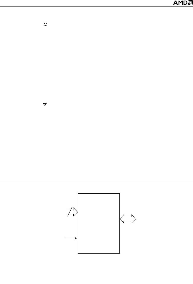
LOGIC SYMBOL
16
A0–A15 |
8 |
DQ0–DQ7
 CE# (E#)
 OE# (G#)
WE# (W#)
18880C-5
Am28F512A |
5 |
ORDERING INFORMATION
Standard Products
AMD standard products are available in several packages and operating ranges. The order number (Valid Combination) is formed by a combination of:
AM28F512A -70 |
J |
C |
B |
OPTIONAL PROCESSING
Blank = Standard Processing
B = Burn-In
Contact an AMD representative for more information.
TEMPERATURE RANGE
C = Commercial (0°C to +70°C)
I = Industrial (–40°C to +85°C)
E = Extended (–55°C to +125°C)
PACKAGE TYPE
P = 32-Pin Plastic DIP (PD 032)
J = 32-Pin Rectangular Plastic Leaded Chip
Carrier (PL 032)
E = 32-Pin Thin Small Outline Package (TSOP)
Standard Pinout (TS 032)
F = 32-Pin Thin Small Outline Package (TSOP)
Reverse Pinout (TSR032)
SPEED OPTION
See Product Selector Guide and Valid Combinations
DEVICE NUMBER/DESCRIPTION
Am28F512A
512 Kilobit (64 K x 8-Bit) 12.0 Volt CMOS Flash Memory with Embedded Algorithms
Valid Combinations
AM28F512A-70
AM28F512A-90
AM28F512A-120
AM28F512A-150
AM28F512A-200
PC, PI, PE, JC, JI, JE, EC, EI, EE, FC, FI, FE
Valid Combinations
Valid Combinations list configurations planned to be supported in volume for this device. Consult the local AMD sales office to confirm availability of specific valid combinations and to check on newly released combinations.
6 |
Am28F512A |

PIN DESCRIPTION
A0–A15
Address Inputs for memory locations. Internal latches hold addresses during write cycles.
CE# (E#)
Chip Enable active low input activates the chip’s control logic and input buffers. Chip Enable high will deselect the device and operates the chip in stand-by mode.
DQ0–DQ7
Data Inputs during memory write cycles. Internal latches hold data during write cycles. Data Outputs during memory read cycles.
NC
No Connect-corresponding pin is not connected internally to the die.
OE# (G#)
Output Enable active low input gates the outputs of the device through the data buffers during memory read cycles. Output Enable is high during command sequencing and program/erase operations.
VCC
Power supply for device operation. (5.0 V ± 5% or 10%)
VPP
Program voltage input. VPP must be at high voltage in order to write to the command register. The command register controls all functions required to alter the memory array contents. Memory contents cannot be altered when VPP ≤ VCC +2 V.
VSS
Ground.
WE# (W#)
Write Enable active low input controls the write function of the command register to the memory array. The target address is latched on the falling edge of the Write Enable pulse and the appropriate data is latched on the rising edge of the pulse. Write Enable high inhibits writing to the device.
Am28F512A |
7 |

BASIC PRINCIPLES
This section contains descriptions about the device read, erase, and program operations, and write operation status of the Am29FxxxA, 12.0 volt family of Flash devices. References to some tables or figures may be given in generic form, such as “Command Definitions table”, rather than “Table 1”. Refer to the corresponding data sheet for the actual table or figure.
The Am28FxxxA family uses 100% TTL-level control inputs to manage the command register. Erase and reprogramming operations use a fixed 12.0 V ± 5% high voltage input.
Read Only Memory
Without high VPP voltage, the device functions as a read only memory and operates like a standard EPROM. The control inputs still manage traditional read, standby, output disable, and Auto select modes.
Command Register
The command register is enabled only when high voltage is applied to the VPP pin. The erase and reprogramming operations are only accessed via the register. In addition, two-cycle commands are required for erase and reprogramming operations. The traditional read, standby, output disable, and Auto select modes are available via the register.
The device’s command register is written using standard microprocessor write timings. The register controls an internal state machine that manages all device operations. For system design simplification, the device is designed to support either WE# or CE# controlled writes. During a system write cycle, addresses are latched on the falling edge of WE# or CE# whichever occurs last. Data is latched on the rising edge of WE# or CE# whichever occur first. To simplify the following discussion, the WE# pin is used as the write cycle control pin throughout the rest of this text. All setup and hold times are with respect to the WE# signal.
OVERVIEW OF ERASE/PROGRAM OPERATIONS
Embedded Erase Algorithm
AMD now makes erasure extremely simple and reliable. The Embedded Erase algorithm requires the user to only write an erase setup command and erase command. The device will automatically pre-program and verify the entire array. The device automatically times the erase pulse width, provides the erase verify and counts the number of sequences. A status bit, Data# Polling, provides feedback to the user as to the status of the erase operation.
Embedded Programming Algorithm
AMD now makes programming extremely simple and reliable. The Embedded Programming algorithm requires the user to only write a program setup command and a program command. The device automatically times the programming pulse width, provides the program verify and counts the number of sequences. A status bit, Data# Polling, provides feedback to the user as to the status of the programming operation.
DATA PROTECTION
The device is designed to offer protection against accidental erasure or programming caused by spurious system level signals that may exist during power transitions. The device powers up in its read only state. Also, with its control register architecture, alteration of the memory contents only occurs after successful completion of specific command sequences.
The device also incorporates several features to prevent inadvertent write cycles resulting from VCC power-up and power-down transitions or system noise.
Low VCC Write Inhibit
To avoid initiation of a write cycle during VCC power-up and power-down, the device locks out write cycles for VCC < VLKO (see DC characteristics section for volt-
ages). When VCC < VLKO, the command register is disabled, all internal program/erase circuits are disabled,
and the device resets to the read mode. The device ignores all writes until VCC > VLKO. The user must ensure that the control pins are in the correct logic state when VCC > VLKO to prevent unintentional writes.
Write Pulse “Glitch” Protection
Noise pulses of less than 10 ns (typical) on OE#, CE# or WE# will not initiate a write cycle.
Logical Inhibit
Writing is inhibited by holding any one of OE# = VIL, CE#=VIH or WE# = VIH. To initiate a write cycle CE# and WE# must be a logical zero while OE# is a logical one.
Power-Up Write Inhibit
Power-up of the device with WE# = CE# = VIL and OE# = VIH will not accept commands on the rising edge of WE#. The internal state machine is automatically reset to the read mode on power-up.
8 |
Am28F512A |

FUNCTIONAL DESCRIPTION
Description Of User Modes
Table 1. Am28F512A Device Bus Operations (Notes 7 and 8)
|
|
CE# |
OE# |
WE# |
VPP |
|
|
|
|
|
Operation |
(E#) |
(G#) |
(W#) |
(Note 1) |
A0 |
A9 |
I/O |
|
|
|
|
|
|
|
|
|
|
|
|
Read |
VIL |
VIL |
X |
VPPL |
A0 |
A9 |
DOUT |
|
|
Standby |
VIH |
X |
X |
VPPL |
X |
X |
HIGH Z |
|
Read-Only |
Output Disable |
VIL |
VIH |
VIH |
VPPL |
X |
X |
HIGH Z |
|
Auto-select Manufacturer |
VIL |
VIL |
VIH |
VPPL |
VIL |
VID |
CODE |
||
|
|||||||||
|
Code (Note 2) |
(Note 3) |
(01h) |
||||||
|
Auto-select Device |
VIL |
VIL |
VIH |
VPPL |
VIH |
VID |
CODE |
|
|
Code (Note 2) |
(Note 3) |
(AEh) |
||||||
|
Read |
VIL |
VIL |
VIH |
VPPH |
A0 |
A9 |
DOUT |
|
|
|
|
|
|
|
|
|
(Note 4) |
|
|
|
|
|
|
|
|
|
|
|
Read/Write |
Standby (Note 5) |
VIH |
X |
X |
VPPH |
X |
X |
HIGH Z |
|
Output Disable |
VIL |
VIH |
VIH |
VPPH |
X |
X |
HIGH Z |
||
|
|||||||||
|
Write |
VIL |
VIH |
VIL |
VPPH |
A0 |
A9 |
DIN |
|
|
|
|
|
|
|
|
|
(Note 6) |
|
|
|
|
|
|
|
|
|
|
Legend:
X = Don’t care, where Don’t Care is either VIL or VIH levels. VPPL = VPP < VCC + 2 V. See DC Characteristics for voltage levels of VPPH. 0 V < An < VCC + 2 V, (normal TTL or CMOS input levels, where n = 0 or 9).
Notes:
1.VPPL may be grounded, connected with a resistor to ground, or < VCC + 2.0 V. VPPH is the programming voltage specified for the device. Refer to the DC characteristics. When VPP = VPPL, memory contents can be read but not written or erased.
2.Manufacturer and device codes may also be accessed via a command register write sequence. Refer to Table 2.
3.11.5 < VID < 13.0 V. Minimum VID rise time and fall time (between 0 and VID voltages) is 500 ns.
4.Read operation with VPP = VPPH may access array data or the Auto select codes.
5.With VPP at high voltage, the standby current is ICC + IPP (standby).
6.Refer to Table 3 for valid DIN during a write operation.
7.All inputs are Don’t Care unless otherwise stated, where Don’t Care is either VIL or VIH levels. In the Auto select mode all addresses except A9 and A0 must be held at VIL.
8.If VCC ≤ 1.0 Volt, the voltage difference between VPP and VCC should not exceed 10.0 volts. Also, the Am28F256 has a VPP rise time and fall time specification of 500 ns minimum.
Am28F512A |
9 |

READ-ONLY MODE
When VPP is less than VCC + 2 V, the command register is inactive. The device can either read array or autoselect data, or be standby mode.
Read
The device functions as a read only memory when VPP < VCC + 2 V. The device has two control functions. Both must be satisfied in order to output data. CE# controls power to the device. This pin should be used for specific device selection. OE# controls the device outputs and should be used to gate data to the output pins if a device is selected.
Address access time tACC is equal to the delay from stable addresses to valid output data. The chip enable access time tCE is the delay from stable addresses and stable CE# to valid data at the output pins. The output enable access time is the delay from the falling edge of OE# to valid data at the output pins (assuming the addresses have been stable at least tACC - tOE).
Standby Mode
The device has two standby modes. The CMOS standby mode (CE# input held at VCC ± 0.5 V), consumes less than 100 µA of current. TTL standby mode (CE# is held at VIH) reduces the current requirements to less than 1 mA. When in the standby mode the outputs are in a high impedance state, independent of the OE# input.
If the device is deselected during erasure, programming, or program/erase verification, the device will draw active current until the operation is terminated.
Output Disable
Output from the device is disabled when OE# is at a logic high level. When disabled, output pins are in a high impedance state.
Auto Select
Flash memories can be programmed in-system or in a standard PROM programmer. The device may be soldered to the circuit board upon receipt of shipment and programmed in-system. Alternatively, the device may initially be programmed in a PROM programmer prior to soldering the device to the board.
The Auto select mode allows the reading out of a binary code from the device that will identify its manufacturer and type. This mode is intended for the purpose of automatically matching the device to be programmed with its corresponding programming algorithm. This mode is functional over the entire temperature range of the device.
Programming In A PROM Programmer
To activate this mode, the programming equipment must force VID (11.5 V to 13.0 V) on address A9. Two identifier bytes may then be sequenced from the device outputs by toggling address A0 from VIL to VIH. All other address lines must be held at VIL, and VPP must be less than or equal to VCC + 2.0 V while using this Auto select mode. Byte 0 (A0 = VIL) represents the manufacturer code and byte 1 (A0 = VIH) the device identifier code. For the device the two bytes are given in the table 2 of the device data sheet. All identifiers for manufacturer and device codes will exhibit odd parity with the MSB (DQ7) defined as the parity bit.
Table 2. Am28F512A Auto Select Code
|
|
Code |
Type |
A0 |
(HEX) |
|
|
|
Manufacturer Code |
VIL |
01 |
Device Code |
VIH |
AE |
10 |
Am28F512A |
ERASE, PROGRAM, AND READ MODE
When VPP is equal to 12.0 V ± 5%, the command register is active. All functions are available. That is, the device can program, erase, read array or autoselect data, or be standby mode.
Write Operations
High voltage must be applied to the VPP pin in order to activate the command register. Data written to the register serves as input to the internal state machine. The output of the state machine determines the operational function of the device.
The command register does not occupy an addressable memory location. The register is a latch that stores the command, along with the address and data information needed to execute the command. The register is written by bringing WE# and CE# to VIL, while OE# is at VIH. Addresses are latched on the falling edge of WE#, while data is latched on the rising edge of the WE# pulse. Standard microprocessor write timings are used.
The device requires the OE# pin to be VIH for write operations. This condition eliminates the possibility for bus contention during programming operations. In order to write, OE# must be VIH, and CE# and WE# must be VIL. If any pin is not in the correct state a write command will not be executed.
Refer to AC Write Characteristics and the Erase/Programming Waveforms for specific timing parameters.
Command Definitions
The contents of the command register default to 00h (Read Mode) in the absence of high voltage applied to the VPP pin. The device operates as a read only memory. High voltage on the VPP pin enables the command register. Device operations are selected by writing specific data codes into the command register. Table 3 in the device data sheet defines these register commands.
Read Command
Memory contents can be accessed via the read command when VPP is high. To read from the device, write 00h into the command register. Standard microprocessor read cycles access data from the memory. The device will remain in the read mode until the command register contents are altered.
The command register defaults to 00h (read mode) upon VPP power-up. The 00h (Read Mode) register default helps ensure that inadvertent alteration of the memory contents does not occur during the VPP power transition. Refer to the AC Read Characteristics and Waveforms for the specific timing parameters.
Table 3. Am28F512A Command Definitions
|
|
First Bus Cycle |
|
|
Second Bus Cycle |
|
|||
|
|
|
|
|
|
|
|
|
|
|
Operation |
Address |
|
Data |
Operation |
|
Address |
|
Data |
Command |
(Note 1) |
(Note 2) |
|
(Note 3) |
(Note 1) |
|
(Note 2) |
|
(Note 3) |
|
|
|
|
|
|
|
|
|
|
Read Memory (Note 4) |
Write |
X |
|
00h/FFh |
Read |
|
RA |
|
RD |
|
|
|
|
|
|
|
|
|
|
Read Auto select |
Write |
X |
|
80h or 90h |
Read |
|
00h/01h |
|
01h/AEh |
|
|
|
|
|
|
|
|
|
|
Embedded Erase Set-up/ |
Write |
X |
|
30h |
Write |
|
X |
|
30h |
Embedded Erase |
|
|
|
||||||
|
|
|
|
|
|
|
|
|
|
|
|
|
|
|
|
|
|
|
|
Embedded Program Set-up/ |
Write |
X |
|
10h or 50h |
Write |
|
PA |
|
PD |
Embedded Program |
|
|
|
||||||
|
|
|
|
|
|
|
|
|
|
|
|
|
|
|
|
|
|
|
|
Reset (Note 4) |
Write |
X |
|
00h/FFh |
Write |
|
X |
|
00h/FFh |
|
|
|
|
|
|
|
|
|
|
Notes:
1.Bus operations are defined in Table 1.
2.RA = Address of the memory location to be read.
PA = Address of the memory location to be programmed. Addresses are latched on the falling edge of the WE# pulse. X = Don’t care.
3.RD = Data read from location RA during read operation.
PD = Data to be programmed at location PA. Data latched on the rising edge of WE#.
4.Please reference Reset Command section.
Am28F512A |
11 |
Loading...