


LM2825N-ADJ
LM2825
Integrated Power Supply 1A DC-DC Converter
General Description
The LM2825 is a complete 1A DC-DC Buck converter pack-
aged in a 24-lead molded Dual-In-Line integrated circuit
package.
Contained within the package are all the active and passive
components for ahighefficiency step-down (buck) switching
regulator. Available in fixed output voltages of 3.3V, 5V and
12V, as well as two adjustable versions, these devices can
provide up to 1A of load current with fully guaranteed electri-
cal specifications.
Self-contained, this converter is also fully protected from out-
put fault conditions, such as excessive load current, short
circuits, or excessive temperatures.
Highlights
n No external components required (fixed output voltage
versions)
n Integrated circuit reliability
n MTBF over 20 million hours
n Radiated EMI meets Class B stipulated by CISPR 22
n High power density, 35 W/in
3
n 24-pin DIP package profile (1.25 x 0.54 x 0.26 inches)
Features
n Minimum design time required
n 3.3V, 5V and 12V fixed output versions
n Two adjustable versions allow 1.23V to 15V outputs
n Wide input voltage range, up to 40V
n Low-power standby mode, I
Q
typically 65 µA
n High efficiency, typically 80
%
n
±
4
%
output voltage tolerance
n Excellent line and load regulation
n TTL shutdown capability/programmable Soft-start
n Thermal shutdown and current limit protection
n −40˚C to +85˚C ambient temperature range
Applications
n Simple high-efficiency step-down (buck) regulator
n On-card switching regulators
n Efficient pre-regulator for linear regulators
n Distributed power systems
n DC/DC module replacement
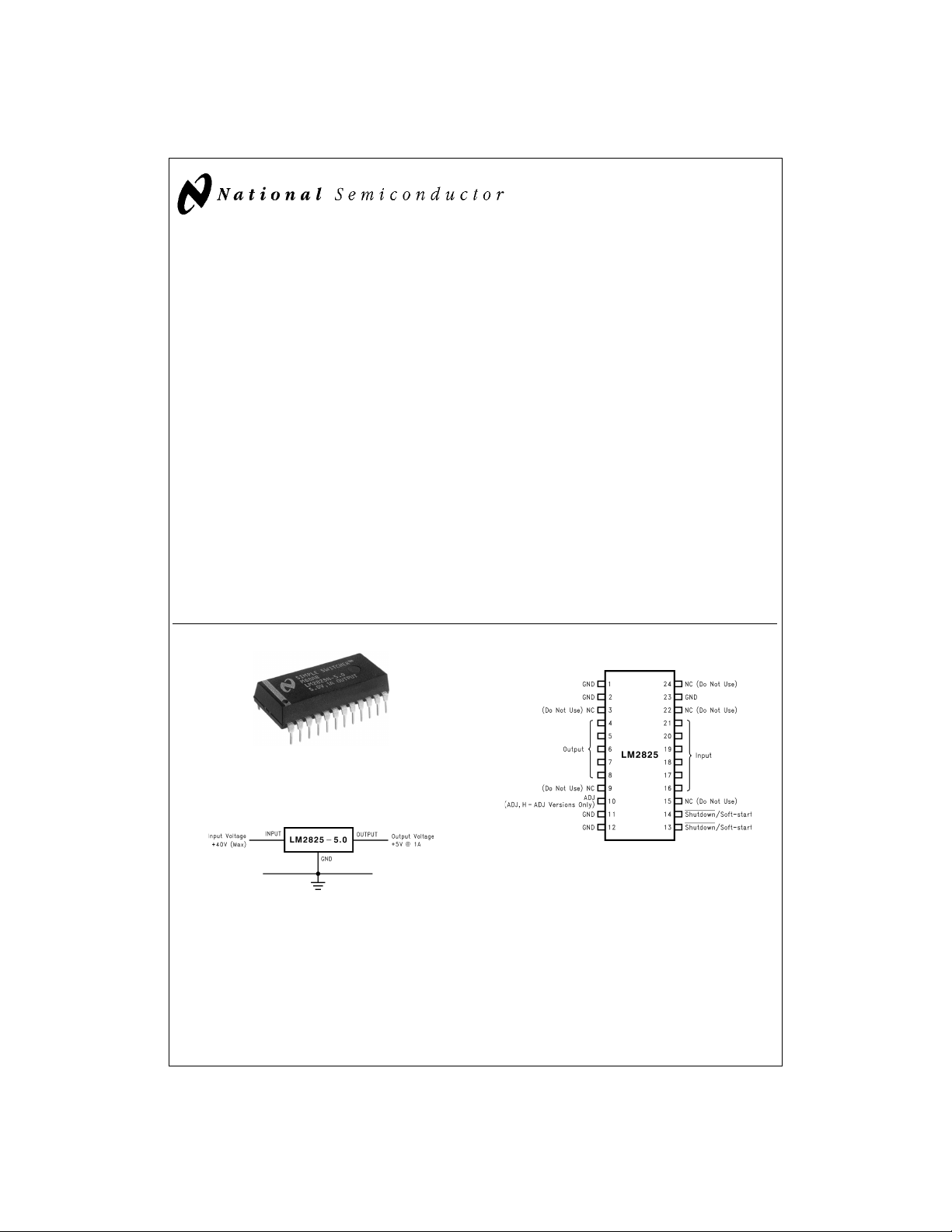
Standard Application
(Fixed output voltage versions)
Radiated EMI
Radiated emission of electromagnetic fields is measured at
10m distance. The emission levels are within the Class B
limits stipulated by CISPR 22.
30. . . .230 MHz 30 dB µV/m
230. . . .1000 MHz 37 dB µV/m
1. . . .10 GHz 46 dB µV/m
Connection Diagram
Ordering Information
Order Number LM2825N-3.3, LM2825N-5.0, LM2825N-12,
LM2825N-ADJ or LM2825HN-ADJ
See NS Package Number NA24F
DS012661-27
DS012661-1
DS012661-2
“NC (Do not use)” pins: See
Figure 11
.
Top View
May 1997
LM2825 Integrated Power Supply 1A DC-DC Converter
© 1997 National Semiconductor Corporation DS012661 www.national.com
Absolute Maximum Ratings (Note 1)
If Military/Aerospace specified devices are required,
please contact the National Semiconductor Sales Office/
Distributors for availability and specifications.
Maximum Input Supply (V
IN
) +45V
SD/SS Pin Input Voltage (Note 2) 6V
Output Pin Voltage
(3.3V, 5.0V and ADJ) −1V ≤ V ≤ 9V
(12V and H-ADJ) −1V ≤ V ≤ 16V
ADJ Pin Voltage (ADJ, H-ADJ only) −0.3V ≤ V ≤ 25V
Power Dissipation Internally Limited
Storage Temperature Range −40˚C to +125˚C
ESD Susceptibility
Human Body Model (Note 3) 2 kV
Lead Temperature (Soldering 10 sec.) 260˚C
Operating Ratings
Ambient Temperature Range −40˚C ≤ T
A
≤ +85˚C
Junction Temperature Range −40˚C ≤ T
J
≤ +125˚C
Input Supply Voltage (3.3V version) 4.75V to 40V
Input Supply Voltage (5V version) 7V to 40V
Input Supply Voltage (12V version) 15V to 40V
Input Supply Voltage (-ADJ, H-ADJ) 4.5V to 40V
LM2825-3.3 Electrical Characteristics (Note 4)
Specifications with standard type face are for T
A
=
25˚C, and those with boldface type apply over full Operating Tempera-
ture Range. Test Circuit
Figure 2
.
Symbol Parameter Conditions LM2825-3.3 Units
(Limits)
Typical Limit
(Note 6) (Note 7)
V
OUT
Output Voltage 4.75V ≤ V
IN
≤ 40V, 0.1A ≤ I
LOAD
≤ 1A 3.3 V
3.168/3.135 V(min)
3.432/3.465 V(max)
Line Regulation 4.75V ≤ V
IN
≤ 40V 1.5 mV
I
LOAD
=
100 mA
Load Regulation 0.1A ≤ I
LOAD
≤ 1A 8 mV
V
IN
=
12V
Output Ripple Voltage V
IN
=
12V, I
LOAD
=
1A 40 mV p-p
η Efficiency V
IN
=
12V, I
LOAD
=
0.5A 75
%
LM2825-5.0 Electrical Characteristics (Note 4)
Specifications with standard type face are for T
A
=
25˚C, and those with boldface type apply over full Operating Tempera-
ture Range. Test Circuit
Figure 2
.
Symbol Parameter Conditions LM2825-5.0 Units
(Limits)
Typical Limit
(Note 6) (Note 7)
V
OUT
Output Voltage 7V ≤ V
IN
≤ 40V, 0.1A ≤ I
LOAD
≤ 1A 5.0 V
4.800/4.750 V(min)
5.200/5.250 V(max)
Line Regulation 7V ≤ V
IN
≤ 40V 2.7 mV
I
LOAD
=
100 mA
Load Regulation 0.1A ≤ I
LOAD
≤ 1A 8 mV
V
IN
=
12V
Output Ripple Voltage V
IN
=
12V, I
LOAD
=
1A 40 mV p-p
η Efficiency V
IN
=
12V, I
LOAD
=
0.5A 80
%
www.national.com 2
LM2825-12 Electrical Characteristics (Note 4)
Specifications with standard type face are for T
A
=
25˚C, and those with boldface type apply over full Operating Tempera-
ture Range. Test Circuit
Figure 2
.
Symbol Parameter Conditions LM2825-12 Units
(Limits)
Typical Limit
(Note 6) (Note 7)
V
OUT
Output Voltage 15V ≤ V
IN
≤ 40V, 0.1A ≤ I
LOAD
≤ 0.75A 12.0 V
11.52/11.40 V(min)
12.48/12.60 V(max)
Line Regulation 15V ≤ V
IN
≤ 40V 8.5 mV
I
LOAD
=
100 mA
Load Regulation 0.1A ≤ I
LOAD
≤ 0.75A 12 mV
V
IN
=
24V
Output Ripple Voltage V
IN
=
24V, I
LOAD
=
1A 100 mV p-p
η Efficiency V
IN
=
24V, I
LOAD
=
0.5A 87
%
LM2825-ADJ Electrical Characteristics (Note 5)
Specifications with standard type face are for T
A
=
25˚C, and those with boldface type apply over full Operating Tempera-
ture Range. Test Circuit
Figure 3
.
Symbol Parameter Conditions LM2825-ADJ Units
(Limits)
Typical Limit
(Note 6) (Note 7)
V
ADJ
Adjust Pin Voltage 4.5V ≤ V
IN
≤ 40V, 0.1A ≤ I
LOAD
≤ 1A 1.230 V
1.23V ≤ V
OUT
≤ 8V 1.193/1.180 V(min)
1.267/1.280 V(max)
η Efficiency V
IN
=
12V, I
LOAD
=
0.5A 74
%
V
OUT
Programmed for 3V. See Circuit of
Figure 3
LM2825H-ADJ Electrical Characteristics (Note 5)
Specifications with standard type face are for T
A
=
25˚C, and those with boldface type apply over full Operating Temperature
Range. Test Circuit
Figure 3
.
Symbol Parameter Conditions LM2825H-ADJ Units
(Limits)
Typical Limit
(Note 6) (Note 7)
V
ADJ
Adjust Pin Voltage 9V ≤ V
IN
≤ 40V, 0.1A ≤ I
LOAD
≤ 0.55A 1.230 V
7V ≤ V
OUT
≤ 15V 1.193/1.180 V(min)
1.267/1.280 V(max)
η Efficiency V
IN
=
24V, I
LOAD
=
0.5A 87
%
V
OUT
Programmed for 12V.
See Circuit of
Figure 3
3 www.national.com
All Output Voltage Versions Electrical Characteristics
Specifications with standard type face are for T
A
=
25˚C, and those with boldface type apply over full Operating Range. Un-
less otherwise specified, V
IN
=
12V for 3.3V, 5.0V and ADJ versions, V
IN
=
24V for 12V and H-ADJ versions, I
LOAD
=
100 mA.
Symbol Parameter Conditions LM2825-XX Units
(Limits)
Typical Limit
(Note 6) (Note 7)
I
CL
DC Output Current
Limit
R
L
=
0Ω 1.4 A
1.2 A(min)
2.4 A(max)
I
Q
Operating Quiescent
Current
SD/SS Pin
=
3.1V 5 mA
(Note 8) 10 mA(max)
I
STBY
Standby Quiescent
Current
SD/SS Pin
=
0V 65 µA
(Note 8) 200 µA(max)
I
ADJ
Adjust Pin Bias Current Adjustable Versions Only, V
FB
=
1.3V 6 nA
50/100 nA(max)
f
O
Oscillator Frequency (Note 9) 150 kHz
θ
JA
Thermal Resistance Junction to Ambient (Note 10) 30 ˚C/W
SHUTDOWN/SOFT-START CONTROL Test Circuit
Figure 2
V
SD
Shutdown Threshold
Voltage
1.3 V
Low (Shutdown Mode) 0.6 V(max)
High (Soft-start Mode) 2.0 V(min)
V
SS
Soft-start Voltage V
OUT
=
20
%
of Nominal Output Voltage 2 V
V
OUT
=
100
%
of Nominal Output Voltage 3
I
SD
Shutdown Current V
SHUTDOWN
=
0.5V
5µA
(Note 8) 10 µA(max)
I
SS
Soft-start Current V
SOFT-START
=
2.5V 1.6 µA
(Note 8) 5 µA(max)
Note 1: Absolute Maximum Ratings indicate limits beyond which damage to the device may occur. Operating Ratings indicate conditions for which the device is in-
tended to be functional, but do not guarantee specific performance limits. For guaranteed specifications and test conditions, see the Electrical Characteristics.
Note 2: Voltage internally clamped. If clamp voltage is exceeded, limit current to a maximum of 5 mA.
Note 3: The human body model is a 100 pF capacitor discharged through a 1.5k resistor into each pin.
Note 4: When the LM2825 is used as shown in
Figure 2
test circuit, system performance will be as shown in Electrical Characteristics.
Note 5: When the LM2825 is used as shown in
Figure 3
test circuit, system performance will be as shown in Electrical Characteristics.
Note 6: Typical numbers are at 25˚C and represent the most likely norm.
Note 7: All limits guaranteed at room temperature (standard type face) and at temperature extremes (bold type face) when output current is limited to the value given
in the temperature derating curves. Seethe application section for curves. All limits at temperature extremes are guaranteed using standard Statistical Quality Control
(SQC) methods. All limits are used to calculate Average Outgoing Quality Level (AOQL).
Note 8: I
LOAD
=
0A.
Note 9: The switching frequency is reduced when the second stage current limit is activated. The amount of reduction is determined by the severity of current over-
load.
Note 10: Junction to ambient thermal resistance (no external heat sink) for the DIP-24 package with the leads soldered to a printed circuit board with (1 oz.) copper
area of approximately 2 in
2
.
www.national.com 4
 Loading...