


NSC LM2936-5.0MDC, LM2936MX-5.0, LM2936MMX-5.0, LM2936MM-5.0, LM2936M-5.0 Datasheet
...
June 2002
LM2936-5.0
Ultra-Low Quiescent Current 5V Regulator
General Description
The LM2936 ultra-low quiescent current regulator features low dropout voltage and low current in the standby mode. With less than 15 µA quiescent current at a 100 µA load, the LM2936 is ideally suited for automotive and other battery operated systems. The LM2936 retains all of the features that are common to low dropout regulators including a low dropout PNP pass device, short circuit protection, reverse battery protection, and thermal shutdown. The LM2936 has a 40V maximum operating voltage limit, a −40˚C to +125˚C operating temperature range, and ±3% output voltage tolerance over the entire output current, input voltage, and temperature range. The LM2936 is available in a TO-92 package, a SO-8 surface mount package, and a TO-252 surface mount power package.
Features
nUltra low quiescent current (IQ ≤ 15 µA for IO = 100 µA)
nFixed 5V, 50 mA output
n±2% Initial output tolerance
n±3% Output tolerance over line, load, and temperature
nDropout voltage typically 200 mV @ IO = 50 mA
nReverse battery protection
n−50V reverse transient protection
nInternal short circuit current limit
nInternal thermal shutdown protection
n40V operating voltage limit
n60V operating voltage limit for LM2936HV
nShutdown Pin available with LM2936BM package
Typical Application
00975901
* Required if regulator is located more than 2" from power supply filter capacitor.
** Required for stability. Must be rated for 10 µF minimum over intended operating temperature range. Effective series resistance (ESR) is critical, see curve. Locate capacitor as close as possible to the regulator output and ground pins. Capacitance may be increased without bound.
Connection Diagrams
TO-252 |
SOT-223 |
00975925 |
00975926 |
Top View |
Top View |
Order Number LM2936DT-5.0 |
Order Number LM2936MP-5.0 |
See NS Package Number TD03B |
See NS Package Number MA04A |
Regulator 5V Current Quiescent Low-Ultra 0.5-LM2936
© 2002 National Semiconductor Corporation |
DS009759 |
www.national.com |
LM2936-5.0
Connection Diagrams (Continued)
8-Pin SO (M) |
8-Pin SO (M) |
00975906 |
00975927 |
|
Top View |
||
Top View |
||
Order Number LM2936M-5.0, LM2936HVMA-5.0 |
Order Number LM2936BM-5.0, LM2936HVBMA-5.0 |
|
See NS Package Number M08A |
See NS Package Number M08A |
|
TO-92 |
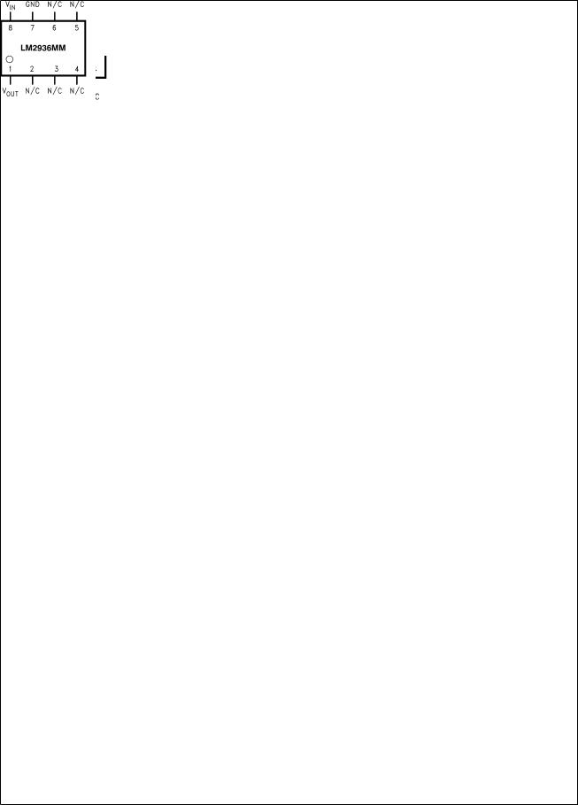
8-Pin Mini SOIC (MM) |
00975902
Bottom View
Order Number LM2936Z-5.0
00975928
See NS Package Number Z03A Top View
Order Number LM2936MM-5.0
See NS Package Number MUA08A
www.national.com |
2 |

Absolute Maximum Ratings (Note 1)
If Military/Aerospace specified devices are required, please contact the National Semiconductor Sales Office/ Distributors for availability and specifications.
Input Voltage (Survival) |
+60V, −50V |
ESD Susceptibility (Note 2) |
2000V |
Power Dissipation (Note 3) |
Internally limited |
Junction Temperature (TJmax) |
150˚C |
Storage Temperature Range |
−65˚C to +150˚C |
Lead Temperature (Soldering, 10 |
|
sec.) |
260˚C |
Operating Ratings
Operating Temperature Range −40˚C to +125˚C
Electrical Characteristics
Maximum Operating Input Voltage - |
|
LM2936 |
+40V |
Maximum Operating Input Voltage - |
|
LM2936HV only |
+60V |
Maximum Shutdown Pin Voltage - |
0V to 40V |
LM2936BM only |
|
TO-92 (Z03A) θJA |
195˚C/W |
MSO-8 (MUA08A) θJA |
200˚C/W |
SO-8 (M08A) θJA |
140˚C/W |
SO-8 (M08A) θJC |
45˚C/W |
TO-252 (TD03B) θJA |
136˚C/W |
TO-252 (TD03B) θJC |
6˚C/W |
SOT-223 (MA04A) θJA |
149˚C/W |
SOT-223 (MA04A) θJC |
36˚C/W |
VIN = 14V, IO = 10 mA, TJ = 25˚C, unless otherwise specified. Boldface limits apply over entire operating temperature range
Parameter |
Conditions |
Min |
Typical |
Max |
Units |
|
(Note 5) |
(Note 4) |
(Note 5) |
||||
|
|
|
||||
|
|
|
|
|
|
|
LM2936HV Only |
|
|
|
|
|
|
|
|
|
|
|
|
|
Output Voltage |
5.5V ≤ VIN ≤ 48V, |
4.85 |
5.00 |
5.15 |
V |
|
|
100 µA ≤ IO ≤ 50 mA (Note 6) |
|||||
|
|
|
|
|
||
Line Regulation |
6V ≤ VIN ≤ 60V, IO = 1mA |
|
15 |
35 |
mV |
|
All LM2936 |
|
|
|
|
|
|
|
|
|
|
|
|
|
|
|
4.90 |
5.00 |
5.10 |
|
|
|
|
|
|
|
|
|
Output Voltage |
5.5V ≤ VIN ≤ 26V, |
4.85 |
5.00 |
5.15 |
V |
|
|
100 µA ≤ IO ≤ 50 mA (Note 6) |
|
|
|
|
|
Quiescent Current |
IO = 100 µA, 8V ≤ VIN ≤ 24V |
|
9 |
15 |
µA |
|
|
IO = 10 mA, 8V ≤ VIN ≤ 24V |
|
0.20 |
0.50 |
mA |
|
|
IO = 50 mA, 8V ≤ VIN ≤ 24V |
|
1.5 |
2.5 |
mA |
|
Line Regulation |
9V ≤ VIN ≤ 16V |
|
5 |
10 |
mV |
|
|
6V ≤ VIN ≤ 40V, IO = 1 mA |
|
10 |
30 |
|
|
Load Regulation |
100 µA ≤ IO ≤ 5 mA |
|
10 |
30 |
mV |
|
|
5 mA ≤ IO ≤ 50 mA |
|
10 |
30 |
|
|
Dropout Voltage |
IO = 100 µA |
|
0.05 |
0.10 |
V |
|
|
IO = 50 mA |
|
0.20 |
0.40 |
V |
|
Short Circuit Current |
VO = 0V |
65 |
120 |
250 |
mA |
|
Output Impedance |
IO = 30 mAdc and 10 mArms, |
|
450 |
|
mΩ |
|
|
f = 1000 Hz |
|
|
|
|
|
Output Noise Voltage |
10 Hz–100 kHz |
|
500 |
|
µV |
|
|
|
|
|
|
|
|
Long Term Stability |
|
|
20 |
|
mV/1000 |
|
|
|
|
|
|
Hr |
|
|
|
|
|
|
|
|
Ripple Rejection |
Vripple = 1Vrms, fripple = 120 Hz |
−40 |
−60 |
|
dB |
|
Reverse Polarity |
RL = 500Ω, T = 1 ms |
−50 |
−80 |
|
V |
|
Transient Input Voltage |
|
|
|
|
|
|
|
|
|
|
|
|
|
Output Voltage with |
VIN = −15V, RL = 500Ω |
|
0.00 |
−0.30 |
V |
|
Reverse Polarity Input |
|
|
|
|
|
|
|
|
|
|
|
|
|
Maximum Line Transient |
RL = 500Ω, VO ≤ 5.5V, T = 40ms |
60 |
|
|
V |
0.5-LM2936
3 |
www.national.com |

LM2936-5.0
Electrical Characteristics (Continued)
VIN = 14V, IO = 10 mA, TJ = 25˚C, unless otherwise specified. Boldface limits apply over entire operating temperature range
Parameter |
Conditions |
Min |
Typical |
Max |
Units |
|
(Note 5) |
(Note 4) |
(Note 5) |
||||
|
|
|
||||
|
|
|
|
|
|
|
Output Bypass |
COUT = 10µF |
0.3 |
|
8 |
Ω |
|
Capacitance (COUT) ESR |
0.1mA ≤ IOUT ≤ 50mA |
|
||||
|
|
|
|
|||
Shutdown Input − LM2936BM Only |
|
|
|
|
||
|
|
|
|
|
|
|
Output Voltage, VOUT |
Output Off, VSD=2.4V, RLOAD = 500Ω |
|
0 |
0.010 |
V |
|
Shutdown High |
Output Off, RLOAD = 500Ω |
2.00 |
1.1 |
|
V |
|
Threshold Voltage, VIH |
|
|
|
|
|
|
Shutdown Low |
Output On, RLOAD = 500Ω |
|
1.1 |
0.60 |
V |
|
Threshold Voltage, VIL |
|
|
|
|
|
|
Shutdown High |
Output Off, VSD = 2.4V, RLOAD = 500Ω |
|
12 |
|
µA |
|
Current, IIH |
|
|
|
|
|
|
Quiescent Current |
Output Off, VSD = 2.4V, RLOAD = 500Ω |
|
30 |
|
µA |
|
|
Includes IIHCurrent |
|
|
|
|
|
Note 1: Absolute Maximum Ratings indicate limits beyond which damage to the device may occur. DC and AC electrical specifications do not apply when operating the device beyond its specified operating ratings.
Note 2: Human body model, 100 pF discharge through a 1.5 kΩ resistor.
Note 3: The maximum power dissipation is a function of TJmax, θJA, and TA. The maximum allowable power dissipation at any ambient temperature is PD = (TJmax − TA)/θJA. If this dissipation is exceeded, the die temperature will rise above 150˚C and the LM2936 will go into thermal shutdown.
Note 4: Typicals are at 25˚C (unless otherwise specified) and represent the most likely parametric norm.
Note 5: Datasheet min/max specification limits are guaranteed by design, test, or statistical analysis.
Note 6: To ensure constant junction temperature, pulse testing is used.
Typical Performance Characteristics
Maximum Power |
|
Dissipation (TO-92) |
Dropout Voltage |
00975907 |
00975908 |
www.national.com |
4 |
 Loading...