


Texas Instruments AM26LS33AMWB, AM26LS33AMJB, AM26LS33AMJ, AM26LS33AMFKB, AM26LS33ACNS Datasheet
...AM26LS32AC, AM26LS33AC, AM26LS32AM, AM26LS33AM
QUADRUPLE DIFFERENTIAL LINE RECEIVERS
|
SLLS115C ± OCTOBER 1980 ± REVISED APRIL 2000 |
|||||||
|
|
|
|
|
|
|
||
D AM26LS32A Meets or Exceeds the |
AM26LS32AC, AM26LS33AC . . . D OR N PACKAGE |
|||||||
Requirements of ANSI EIA/TIA-422-B, |
AM26LS32AM, AM26LS33AM . . . J PACKAGE |
|||||||
EIA/TIA-423-B, and ITU Recommendations |
|
(TOP VIEW) |
|
|
||||
|
|
|
|
|
|
|
|
|
V.10 and V.11 |
1B |
|
1 |
16 |
|
|
VCC |
|
|
|
|
||||||
D AM26LS32A Has ±7-V Common-Mode |
|
|
|
|||||
|
|
|
|
|
||||
1A |
|
2 |
15 |
|
|
4B |
||
Range With ±200-mV Sensitivity |
|
|
|
|||||
1Y |
|
3 |
14 |
|
|
4A |
||
|
|
|
||||||
D AM26LS33A Has ±15-V Common-Mode |
|
|
|
|||||
G |
|
4 |
13 |
|
|
4Y |
||
|
|
|
||||||
Range With ±500-mV Sensitivity |
|
|
5 |
12 |
|
|
|
|
2Y |
|
|
|
G |
|
|||
D Input Hysteresis . . . 50 mV Typical |
2A |
|
6 |
11 |
|
|
3Y |
|
|
|
|
||||||
D Operates From a Single 5-V Supply |
2B |
|
7 |
10 |
|
|
3A |
|
|
|
|
||||||
|
8 |
9 |
|
|
||||
D Low-Power Schottky Circuitry |
GND |
|
|
|
3B |
|||
|
|
|
|
|
|
|
|
|
D3-State Outputs
D Complementary Output-Enable Inputs |
AM26LS32AM, AM26LS33AM . . . FK PACKAGE |
D Input Impedance . . . 12 kΩ Min |
|
(TOP VIEW) |
|
|
|||
|
|
|
NC |
CC |
|
|
|
D Designed to Be Interchangeable With |
|
1A |
1B |
4B |
|
||
|
V |
|
|||||
Advanced Micro Devices AM26LS32 and |
|
3 |
2 |
1 |
20 19 |
|
|
AM26LS33 |
1Y |
4A |
|||||
|
4 |
|
|
|
18 |
||
description |
G |
5 |
|
|
|
17 |
4Y |
NC |
6 |
|
|
|
16 |
NC |
|
|
|
|
|
||||
The AM26LS32A and AM26LS33A devices are |
2Y |
7 |
|
|
|
15 |
G |
2A |
8 |
|
|
|
14 |
3Y |
|
quadruple differential line receivers for balanced |
|
|
|
||||
|
9 |
10 11 12 13 |
|
||||
and unbalanced digital data transmission. The |
|
|
|||||
|
|
|
|
|
|
|
|
enable function is common to all four receivers |
|
2B |
GND |
NC |
3B |
3A |
|
and offers a choice of active-high or active-low |
|
|
|||||
input. The 3-state outputs permit connection |
NC ± No internal connection |
|
|||||
directly to a bus-organized system. Fail-safe |
|
|
|
|
|
|
|
design ensures that, if the inputs are open, the |
|
|
|
|
|
|
|
outputs are always high. |
|
|
|
|
|
|
|
Compared to the AM26LS32 and the AM26LS33, the AM26LS32A and AM26LS33A incorporate an additional stage of amplification to improve sensitivity. The input impedance has been increased, resulting in less loading of the bus line. The additional stage has increased propagation delay; however, this does not affect interchangeability in most applications.
The AM26LS32AC and AM26LS33AC are characterized for operation from 0°C to 70°C. The AM26LS32AM and AM26LS33AM are characterized for operation over the full military temperature range of ±55°C to 125°C.
Please be aware that an important notice concerning availability, standard warranty, and use in critical applications of Texas Instruments semiconductor products and disclaimers thereto appears at the end of this data sheet.
AM26LS32 and AM26LS33 are trademarks of Advanced Micro Devices, Inc.
PRODUCTION DATA information is current as of publication date. Products conform to specifications per the terms of Texas Instruments standard warranty. Production processing does not necessarily include testing of all parameters.
Copyright 2000, Texas Instruments Incorporated
POST OFFICE BOX 655303 •DALLAS, TEXAS 75265 |
1 |
AM26LS32AC, AM26LS33AC, AM26LS32AM, AM26LS33AM QUADRUPLE DIFFERENTIAL LINE RECEIVERS
SLLS115C ± OCTOBER 1980 ± REVISED APRIL 2000
FUNCTION TABLE |
|
||||
(each receiver) |
|
|
|
||
|
|
|
|
|
|
DIFFERENTIAL |
ENABLES |
OUTPUT |
|||
A ± B |
G |
|
Y |
||
G |
|
||||
|
|
|
|
||
VID ≥ VIT+ |
H |
X |
H |
||
X |
L |
H |
|||
|
|||||
|
|
|
|
||
VIT± ≤ VID ≤ VIT+ |
H |
X |
? |
||
X |
L |
? |
|||
|
|||||
|
|
|
|
||
VID ≤ VIT± |
H |
X |
L |
||
X |
L |
L |
|||
|
|||||
|
|
|
|
||
X |
L |
H |
Z |
||
|
|
|
|
||
Open |
H |
X |
H |
||
X |
L |
H |
|||
|
|||||
|
|
|
|
|
|
H = high level, L = low level, ? = indeterminate, |
|||||
X = irrelevant, Z = high impedance (off) |
|
||||
logic symbol²
4 |
|
≥ 1 |
|
|
|
|
|||||
|
G |
|
|
EN |
|
|
|||||
|
|
|
|
||||||||
|
|
12 |
|
|
|
|
|
|
|||
|
G |
|
|
|
|
|
|
|
|
|
|
|
|
|
|
|
|
|
|
|
|||
2 |
|
|
|
|
|
|
3 |
|
|||
|
|
|
|
|
|
|
|||||
1A |
|
|
|
|
|
|
|
1Y |
|||
|
|
|
|
|
|
|
|||||
1 |
|
|
|
|
|
|
|
||||
|
|
|
|
|
|
|
|||||
1B |
|
|
|
|
|
|
|
|
|
||
|
|
|
|
|
|
|
|
|
|||
6 |
|
|
|
|
|
|
5 |
|
|||
|
|
|
|
|
|
|
|||||
2A |
|
|
|
|
|
2Y |
|||||
|
|
|
|
|
|
|
|||||
7 |
|
|
|
|
|
|
|
||||
|
|
|
|
|
|
|
|||||
2B |
|
|
|
|
|
|
|
|
|
||
|
|
|
|
|
|
|
|
|
|||
10 |
|
|
|
|
|
|
11 |
|
|||
|
|
|
|
|
|
|
|||||
3A |
|
|
|
|
|
3Y |
|||||
|
|
|
|
|
|
|
|||||
9 |
|
|
|
|
|
|
|
||||
|
|
|
|
|
|
|
|||||
3B |
|
|
|
|
|
|
|
|
|
||
|
|
|
|
|
|
|
|
|
|||
14 |
|
|
|
|
|
|
13 |
|
|||
|
|
|
|
|
|
|
|||||
4A |
|
|
|
|
|
4Y |
|||||
|
|
|
|
|
|
|
|||||
15 |
|
|
|
|
|
|
|
||||
|
|
|
|
|
|
|
|||||
4B |
|
|
|
|
|
|
|
|
|
||
|
|
|
|
|
|
|
|
|
|||
|
|
|
|
|
|
|
|
|
|
|
|
² This symbol is in accordance with ANSI/IEEE Std 91-1984 and IEC Publication 617-12. Pin numbers shown are for D, J, and N packages.
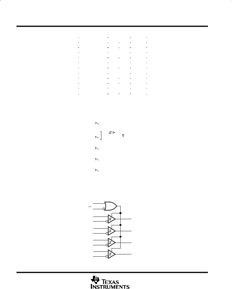
logic diagram (positive logic)
G |
4 |
|
|
|
12 |
|
|
||
G |
|
|
||
|
|
|
||
1A |
2 |
3 |
|
|
1 |
1Y |
|||
1B |
|
|||
|
|
|
||
2A |
6 |
5 |
|
|
7 |
2Y |
|||
2B |
|
|||
|
|
|
||
3A |
10 |
11 |
|
|
9 |
3Y |
|||
3B |
|
|||
|
|
|
||
4A |
14 |
13 |
|
|
15 |
4Y |
|||
4B |
|
|||
|
|
|
2 |
POST OFFICE BOX 655303 •DALLAS, TEXAS 75265 |

AM26LS32AC, AM26LS33AC, AM26LS32AM, AM26LS33AM
QUADRUPLE DIFFERENTIAL LINE RECEIVERS
SLLS115C ± OCTOBER 1980 ± REVISED APRIL 2000
schematics of inputs and outputs
EQUIVALENT OF EACH |
|
|
||
DIFFERENTIAL INPUT |
EQUIVALENT OF EACH ENABLE INPUT |
TYPICAL OF ALL OUTPUTS |
||
VCC |
|
VCC |
VCC |
|
|
|
8.3 kΩ |
85 Ω |
|
|
|
NOM |
||
|
|
NOM |
||
|
|
|
||
100 kΩ |
|
|
|
|
A Input Only |
|
|
|
|
20 kΩ |
960 Ω |
Enable |
|
|
NOM |
|
|||
NOM |
Output |
|||
|
|
|||
Input |
960 Ω |
|
|
|
|
|
|
||
100 kΩ |
NOM |
|
|
|
B Input Only |
|
|
|
|
absolute maximum ratings over operating free-air temperature range (unless otherwise noted)²
Supply voltage, VCC (see Note 1) . . . . . . . . . . . . . . . . . . . . . . . . . . . . . . . . . . . . . . . |
. . . . . . . . . . . . |
. . . . . . . . . . 7 |
V |
Input voltage, VI: Any differential input . . . . . . . . . . . . . . . . . . . . . . . . . . . . . . . . . . . |
. . . . . . . . . . . . |
. . . . . . . . ±25 |
V |
Other inputs . . . . . . . . . . . . . . . . . . . . . . . . . . . . . . . . . . . . . . . . . . |
. . . . . . . . . . . . |
. . . . . . . . . . 7 |
V |
Differential input voltage, VID (see Note 2) . . . . . . . . . . . . . . . . . . . . . . . . . . . . . . . |
. . . . . . . . . . . . |
. . . . . . . . ±25 |
V |
Continuous total power dissipation . . . . . . . . . . . . . . . . . . . . . . . . . . . . . . . . . . . . . |
See Dissipation Rating Table |
||
Package thermal impedance, θJA (see Note 3): D package . . . . . . . . . . . . . . . . . |
. . . . . . . . . . . . |
. . . . . . 73°C/W |
|
N package . . . . . . . . . . . . . . . . . |
. . . . . . . . . . . . |
. . . . . . 67°C/W |
|
Lead temperature 1,6 mm (1/16 inch) from case for 10 seconds: D or N package . . . . . . . . . |
. . . . . . . 260°C |
||
Lead temperature 1,6 mm (1/16 inch) from case for 60 seconds: J package . . |
. . . . . . . . . . . . |
. . . . . . . 300°C |
|
Case temperature for 60 seconds, TC: FK package . . . . . . . . . . . . . . . . . . . . . . . |
. . . . . . . . . . . . |
. . . . . . . 260°C |
|
Storage temperature range, Tstg . . . . . . . . . . . . . . . . . . . . . . . . . . . . . . . . . . . . . . . . |
. . . . . . . . . . . |
±65°C to 150°C |
|
²Stresses beyond those listed under ªabsolute maximum ratingsº may cause permanent damage to the device. These are stress ratings only, and functional operation of the device at these or any other conditions beyond those indicated under ªrecommended operating conditionsº is not implied. Exposure to absolute-maximum-rated conditions for extended periods may affect device reliability.
NOTES: 1. All voltage values, except differential voltages, are with respect to the network ground terminal.
2.Differential voltage values are at the noninverting (A) input terminals with respect to the inverting (B) input terminals.
3.The package thermal impedance is calculated in accordance with JESD 51.
DISSIPATION RATING TABLE
|
PACKAGE |
TA ≤ 25°C |
DERATING FACTOR |
TA = 70°C |
TA = 125°C |
|
|
POWER RATING |
ABOVE TA = 25°C |
POWER RATING |
POWER RATING |
|
|
|
|
|
||||
|
FK |
1375 mW |
11.0 mW/°C |
880 mW |
275 mW |
|
|
J |
1375 mW |
11.0 mW/°C |
880 mW |
275 mW |
|
|
|
|
|
|
|
|
|
|
|
|
|
|
|
|
|
|
|
|
|
|
POST OFFICE BOX 655303 •DALLAS, TEXAS 75265 |
3 |
 Loading...