


MDR-RF915R
Table of contents
 Loading...
MDR-RF915R/RF945R
SERVICE MANUAL
Ver 1.0 2001. 05
Photo : MDR-RF945R
MDR-RF915R is the component model block one in the MDR-RF915RK.
MDR-RF945R is the component model block one in the MDR-RF945RK.
COMPONENT MODEL NAME FOR MDR-RF915RK/
MDR-RF945RK
MDR-RF915RK MDR-RF945RK
Wireless Stereo Headphones MDR-RF915R MDR-RF945
Transmitter TMR-RF915R TMR-RF945
US Model
Canadian Model
SPECIFICATIONS
Headphones
Power source DC 2.4 V: Built-in rechargeable
battery
Mass Approx. 240 g (8.5 oz.) incl.
built-in rechargeable battery
Built-in Ni-Cd rechargeable battery
Model name NC-AA
Voltage 1.2 V
Capacity 700 mAh
Design and specifications are subject to change without
notice.
HEADPHONES
9-873-137-11
2001E0200-1
© 2001.5
Sony Corporation
Personal Audio Company
Shinagawa Tec Service Manual Production Group
MDR-RF915R/RF945R
f
TABLE OF CONTENTS
Specifications ............................................................................ 1
1. GENERAL ....................................................................... 2
2. DISASSEMBLY
2-1. RX-BASE Board ...................................................... 3
3-5. Free Run Frequency
Check and Adjustment (MRD-RF945R).........6
3-6. Receive Frequency
Check and Adjustment (MRD-RF945R)......... 6
3-7. Carrier Modulation Check (MRD-RF945R) ............... 6
3-8. Separation Check (MRD-RF945R) ............................. 6
3. ELECTRICAL ADJUSTMENTS..............................4
3-1. Free Run Frequency
Check and Adjustment (MRD-RF915R) ....... 5
3-2. Receive Frequency
Check and Adjustment (MRD-RF915R) ....... 5
3-3. Carrier Modulation Check (MRD-RF915R) ............. 5
3-4. Separation Check (MRD-RF915R) ........................... 5
SECTION 1
GENERAL
A
5
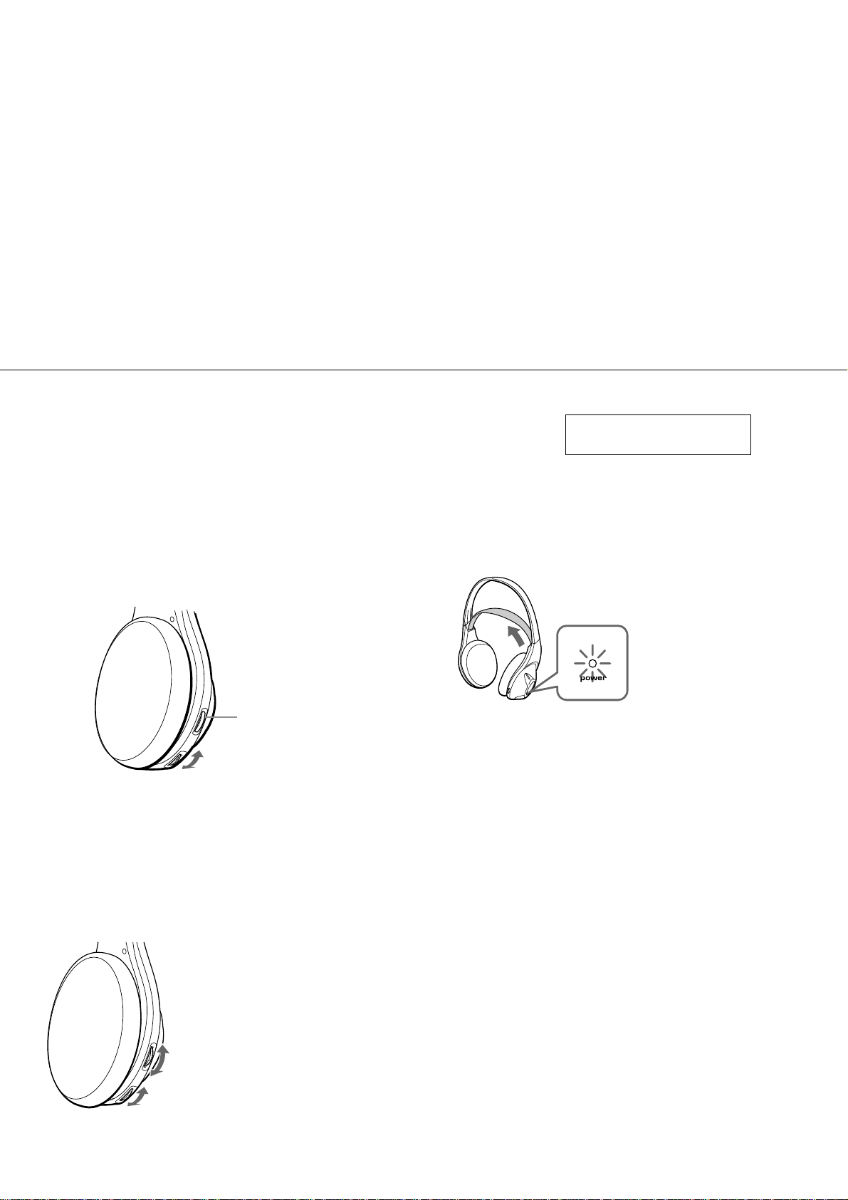
- Turn up the volume to a moderate
level with the VOL control.
Press the TUNING button briefly for
automatic tuning of the headphones.
If you do not receive a clear audio
signal, press it again.
A
MDR-RF945RK
4. DIAGRAMS
4-1. Block Diagrams ........................................................... 8
4-2. Schematic Diagram ..................................................... 9
4-3. Printed Wiring Board................................................. 10
5. EXPLODED VIEWS........................................................11
6. ELECTRICAL PARTS LIST........................................12
This section is extracted from
instruction manual.
Auto power on/off function
When you remove the headphones from your
head, the power turns off automatically. Do not
allow the self adjusting band to be pulled up,
otherwise the headphones will be switched on.
TUNING
button
VOL control
B
5
- Turn up the volume to a moderate
level with the VOL control, then tune
the headphones in to the frequency o
the transmitter with the TUNING
control until you can hear the audio
signal loud and clear.
MDR-RF915RK
B
TUNING
control
VOL control
Try the above steps 3 and 5 until the
receiving performance becomes better.
2
The power turns on.
SAFETY CHECK-OUT
After correcting the original service problem, perform the
following safety checks before releasing the set to the
customer.
1. Check the area of your repair for unsoldered or poorly-sol
deredconnections. Check the entire board surface for solder
splashes and bridges.
2. Check the interboard wiring to ensure that no wires are
“pinched” or contact high-wattage resistors.
3. Look for unauthorized replacement parts, particularlyt ransis
tors, that were installed during a previous repair.
Point them out to the customer and recommend their
replacement.
4. Look for parts which, through functioning, show obvious
signs of deterioration. Point them out to the customer
and recommend their replacement.
5. Check the B+ voltage to see it is at the values specified.
6. Flexible Circuit Board Repairing
• Keep the temperature of the soldering iron around 270°C
during repairing.
• Do not touch the soldering iron on the same conductor of
the circuit board (within 3 times).
• Be careful not to apply force on the conductor when
soldering
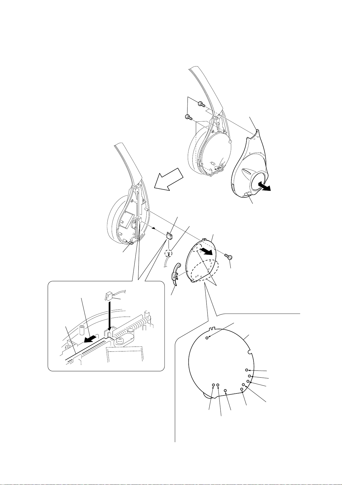
• This set can be disassembled in the order shown below.
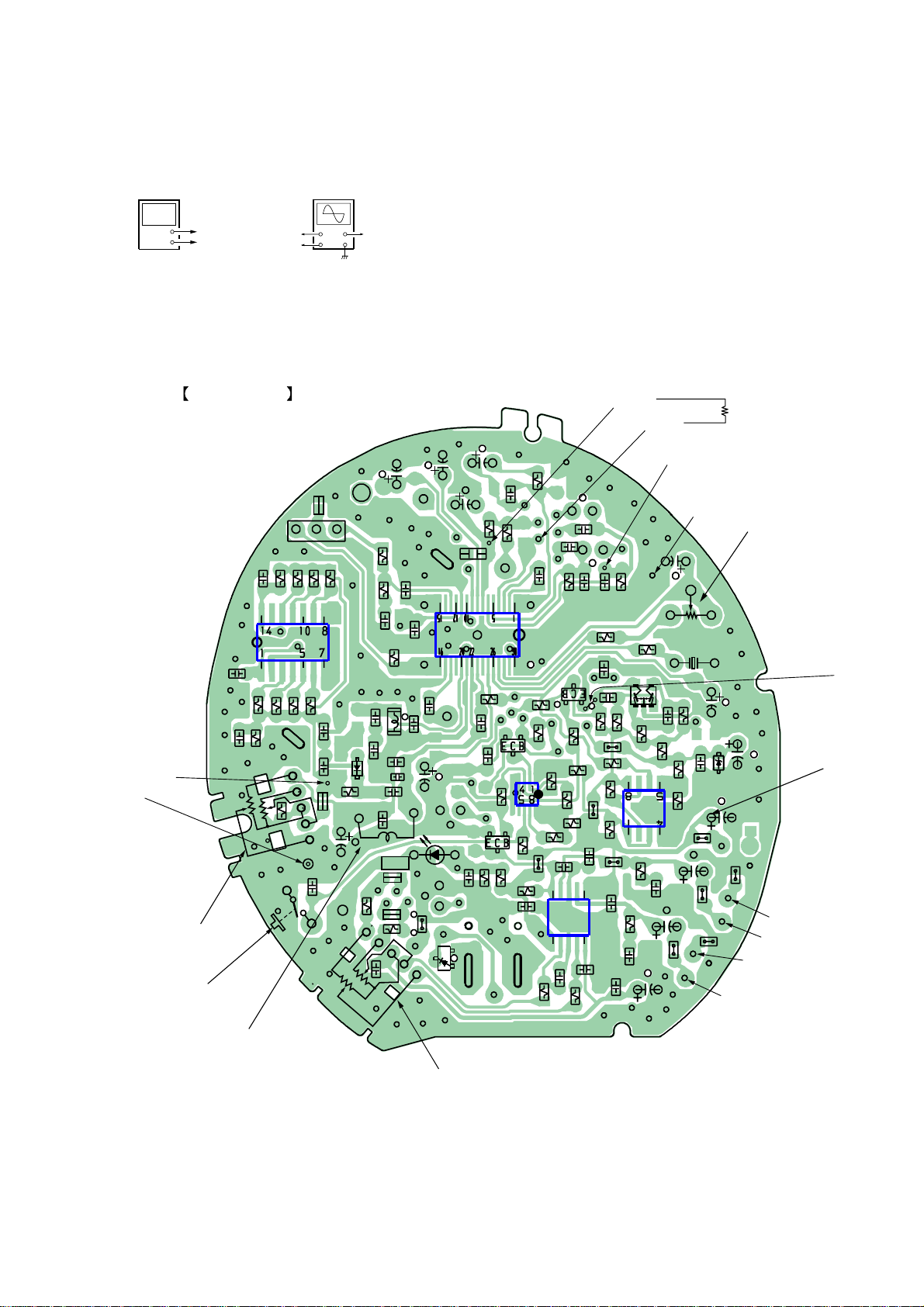
2-1. RX-BASE BOARD
1
SECTION 2
DISASSEMBLY
Five screws (P 2
× 6)
MDR-RF915R/RF945R
Cover (R), hanger
Claw
Precaution for installtion
1
Slide the suspender in the
direction of the arrow.
Suspender
2
Set the psuh
switch (1 key).
8
6
(RF945R)
q;
Switch, push (1 key)
9
Remove the two solderings.
Button, tuning
7
RX-BASE board
5
3
Remove the
nine solderings.
2
Claw
4
Screw (P 2
× 8)
Precaution for installtion
No.205
RX-BASE board
No.204
No.201
No.201 (green)
No.202
No.203
No.203 (black)
Solder the each lead wires directly to the position as shown
while being cautions of colors.
No.204
No.202 (red)
3
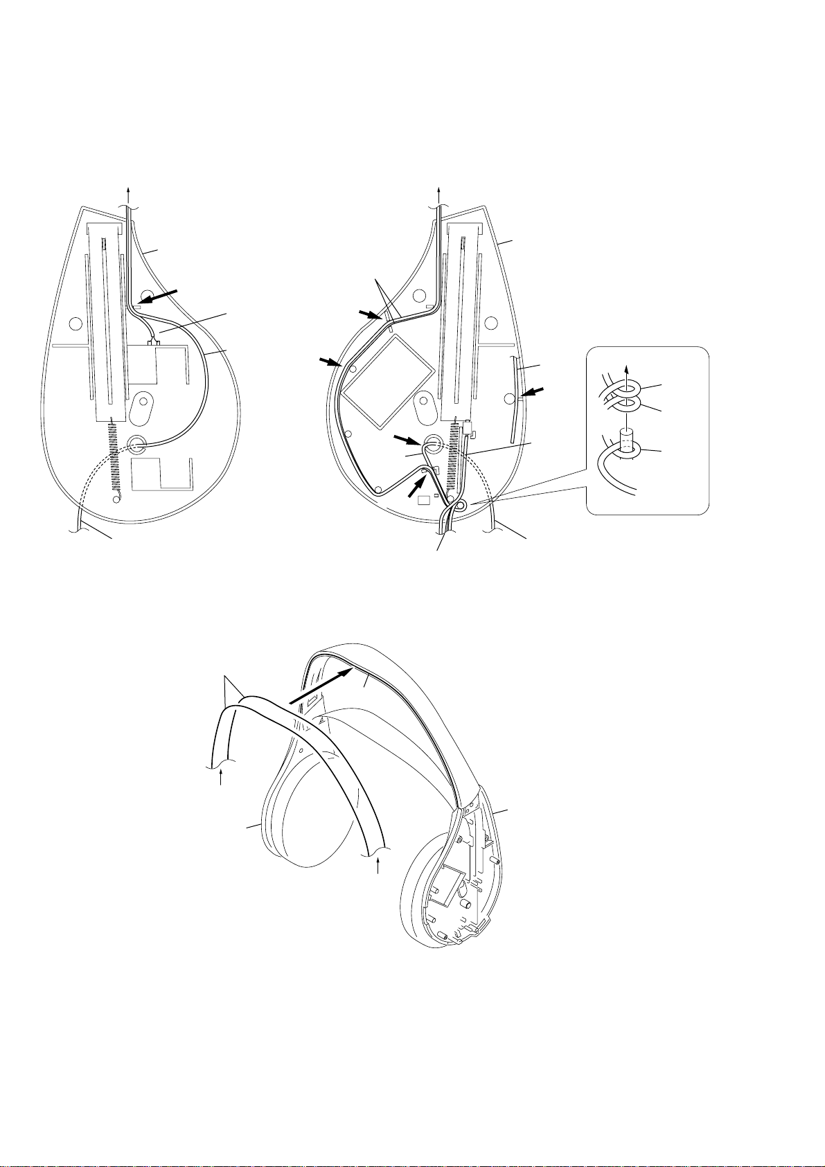
MDR-RF915R/RF945R
Set the lead wires
Set the each lead wires as illustrated below.
B
Cover (L), hanger
Groove
To the driver (030F032).
No.203
No.201
Groove
No.201, No.203
Groove
Groove
No.202
Groove
To the RX-BASE board
A
Cover (R), hanger
No.205
Groove
No.204
To the driver (030F032).
No.201
No.203
No.202
No.201, No.203
B
Cover (L), hanger
Groove
Cover (R), hanger
A
4

SECTION 3
4
+
–+–
IC301 pin6
IC301 pin4
OSCILLOSCPE
CH1 CH2
4
MRD-RF915R
Notes:
1. Use transmitter with check and adjustment alreadycompleted.
2. On adjusting the headphones section, use the transmitter as a
jig.
Headphones:MDR-RF915R
Transmitter:TMR-RF915R
ELECTRICAL ADJUSTMENTS
MDR-RF915R/RF945R
Setting :
Procedure:
1. Connect an oscillator with attenuator and terminator (600 Ω)
2. Connect an AC adapter to the transmitter DC IN 9V jack (J404).
3. Connect a DC 2.4V to the +B power line externally.
4. Connect lead wires to IC301 pin 4, pin 6, pin 7 and GND on
5. Connect a resistor 33k Ω between IC301 pin 4 and pin 7.
6. Connect lead wires to the speakers’ terminals (L+,L-,R+,R-)
3-1. Free Run Frequency Check and Adjustment
1. Set the transmitter AUDIO IN-A connector (J402) to no signal.
Note: In this case, operation time is about 5 or 10 minutes.
2. Check the transmitter power indicator (red) lights.
3. Set the transmitter CHANNEL switch to 1.
4. Set the RV303 (TUNE) to the center position.
5. Connect a frequency counter to IC301 pin 4 and GND on the
6. When the frequency dose not satisfy the specified value, adjust
7. Remove a 33 Ω resister between IC301 pin 4 and pin 7.
Setting :
3-2. Receive Frequency Check and Adjustment
1. Set the transmitter CHANNEL switch to 2.
2. Set the transmitter NOISE FILTER switch to OFF.
3. Input a signal of 1kHz, 316mVrms to transmitter AUDIO IN-
4. Keep distance between transmitter and headphones to 5 meters
5. Set the headphones volume (RV302) to minimum.
6. Set the RV303 (TUNE) to the center position.
7. Connect an oscilloscope CH1 and CH2 to IC301 pin 6 and
8. Check the waveform of the oscilloscope to CH1 is demodulated
9. If CH1 and CH2 are not satisfied in step 8, adjust the coil (L301)
10. Set the transmitter CHANNEL switch to 1.
11. Adjust the RV303 (TUNE) to receive a signal.
12. Check same step 8.
13. Set the transmitter CHANNEL switch to 3.
14. Adjust the RV303 (TUNE) to receive a signal.
15. Check same step 8.
to the transmitter AUDIO IN-A connector (J402).
the RX-BASE board.
on the RX-BASE board.
Perform confirmation for less than 5 minutes.
RX-BASE board, then confirm the frequency within 76kHz
± 50Hz
the value of the frequency counter to specification by RV301
on the RX-BASE board.
Specified values: 76kHz ± 50Hz.
Frequency counter
+
–
IC301 pin
A(L-ch) connector only.
over.
pin 4.
1kHz signal and CH2 is GND.
on the RX board to satisfied step 8.
Confirm the signal with stereo.
Confirm the signal with stereo.
3-3. Carrier Modulation Check
1. Set the transmitter CHANNEL switch to 2.
2. Set the transmitter NOISE FILTER switch to OFF.
3. Input a signal of 1kHz, 316mVrms to transmitter AUDIO IN-A
(L-ch) connector only.
4. Set the headphones volume (RV302) to minimum.
5. Connect an oscilloscope CH1 and CH2 to IC301 pin 6 and
pin 4.
6. Adjust the tuning control (RV303) to receive radio frequency.
7. Check the waveform of the oscilloscope that the CH1 is
demodulated 1kHz signal and CH2 is GND.
8. Connect an AC voltmeter with LPF to IC301 pin 6 and GND.
9. Check the value of the AC voltmeter to 26mVrms ± 2mV
Setting :
Digital voltmeter
(AC range)
+
–
LPF
2.2K
33000P
IC301
pin6
OSCILLOSCPE
IC301 pin6
CH1 CH2
+
–+–
IC301 pin4
3-4. Separation Check
1. Set the transmitter CHANNEL switch to 2.
2. Set the transmitter NOISE FILTER switch to OFF.
3. Input a signal of 1kHz, 316mVrms to transmitter AUDIO IN-A
(L-ch) connector only.
4. Connect an oscilloscope CH1 to speakers terminal (L+,L-) and
CH2 to IC301 pin 4 and GND.
5. Adjust the tuning control (RV303) to receive radio frequency.
6. Check the waveform of the oscilloscope that the CH1 is
demodulated 1kHz signal and CH2 is GND.
7. Connect an AC voltmeter with LPF to speakers terminal (L+,L).
8. Adjust the value of the AC voltmeter to specification by
headphones volume RV302.
Specified values: 155mVrms
9. Connect an AC voltmeter with LPF to speakersterminal
(R+,R-).
10. Measure the value of the AC voltmeter.
11. Check the difference of the L and R to more than 20dB.
12. Input a signal of 1kHz, 316mVrms to transmitter AUDIO IN-A
(R-ch) connector only.
13. Connect an AC voltmeter with LPF to speakers terminal
(R+,R-).
14. Adjust the value of the AC voltmeter to specification by
headphones volume RV302.
Specified values: 155mVrms
15. Connect an AC voltmeter with LPF to speakers terminal
(L+,L-).
16. Measure the value of the AC voltmeter.
17. Check the difference of the L and R to more than 20dB.
Setting :
Digital voltmeter
(AC range)
+
–
L+ / R+
L– / R–
OSCILLOSCPE
CH1 CH2
+
L+
–+–
L–
IC301 pin
5
MDR-RF915R/RF945R
4
4
MRD-RF945R
Notes:
1. Use transmitter with check and adjustment alreadycompleted.
2. On adjusting the headphones section, use the transmitter as a
jig.
Headphones:MDR-RF945R
Transmitter:TMR-RF945R
Procedure:
1. Connect an oscillator with attenuator and terminator (600 Ω)
to the transmitter AUDIO IN-A connector (J402).
2. Connect an AC adapter to the transmitter DC IN 9V jack (J404).
3. Short between Q303 corrector and GND on the RX board.
4. Connect a DC 2.4V to the +B power line externally.
5. Connect lead wires to IC301 pin 4, pin 6, pin 7 and GND on
the RX-BASE board.
6. Connect a resistor 33k Ω between IC301 pin 4 and pin 7.
7. Connect lead wires to the speakers’ terminals (L+,L-,R+,R-)
on the RX-BASE board.
3-5. Free Run Frequency Check and Adjustment
1. Set the transmitter AUDIO IN-A connector (J402) to no signal.
Note: In this case, operation time is about 5 or 10 minutes.
Perform confirmation for less than 5 minutes.
2. Check the transmitter power indicator (red) lights.
3. Set the transmitter CHANNEL switch to 1.
4. Connect DC 1.2V across TP and GND.
5. Connect a frequency counter to IC301 pin 4 and GND on the
RX-BASE board, then confirm the frequency within 76kHz
± 50Hz
6. When the frequency dose not satisfy the specified value, adjust
the value of the frequency counter to specification by RV301
on the RX-BASE board.
Specified values: 76kHz ± 50Hz.
7. Remove a 33 Ω resister between IC301 pin 4 and pin 7.
Setting :
Regulated power supply
(DC 1.2V)
TP
+
–
OSCILLOSCPE
IC301 pin6
CH1 CH2
+
–+–
IC301 pin
3-6. Receive Frequency Check and Adjustment
1. Set the transmitter CHANNEL switch to 2.
2. Set the transmitter NOISE FILTER switch to OFF.
3. Input a signal of 1kHz, 316mVrms to transmitter AUDIO INA(L-ch) connector only.
4. Keep distance between transmitter and headphones to 5 meters
over.
5. Set the headphones volume (RV302) to minimum.
6. Set the RV303 (TUNE) to the center position.
7. Connect an oscilloscope CH1 and CH2 to IC301 pin 6 and
pin 4.
8. Check the waveform of the oscilloscope to CH1 is demodulated
1kHz signal and CH2 is GND.
9. If CH1 and CH2 are not satisfied in step 8, adjust the coil (L301)
on the RX board to satisfied step 8.
10. Open between Q303 corrector and GND on the RX board.
11. When the transmitter off, check the waveform of the oscilloscope
as follows:
1.8V
GND
2-3sec
6
0.6V
12. Set the transmitter CHANNEL switch to 1.
13. Push the headphones tuning switch (S301) to receive radio
frequency.
14. Check same step 8.
15. Set the transmitter CHANNEL switch to 3.
16. Push the headphones tuning switch (S301) to receive radio
frequency.
17. Check same step 8.
Setting :
Regulated power supply
(DC 1.2V)
TP
+
–
OSCILLOSCPE
IC301 pin6
CH1 CH2
+
–+–
IC301 pin
3-7. Carrier Modulation Check
1. Set the transmitter CHANNEL switch to 2.
2. Set the transmitter NOISE FILTER switch to OFF.
3. Input a signal of 1kHz, 316mVrms to transmitter AUDIO IN-A
(L-ch) connector only.
4. Set the headphones volume (RV302) to minimum.
5. Connect an oscilloscope CH1 and CH2 to IC301 pin 6 and
pin 4.
6. Push the headphone tuning switch (S301) to receive radio
frequency.
7. Check the waveform of the oscilloscope that the CH1 is
demodulated 1kHz signal and CH2 is GND.
8. Connect an AC voltmeter with LPF to IC301 pin 6 and GND.
9. Check the value of the AC voltmeter to 26mVrms ± 2mV
Setting :
Digital voltmeter
(AC range)
+
–
LPF
2.2K
33000P
IC301
pin6
OSCILLOSCPE
IC301 pin6
CH1 CH2
+
–+–
IC301 pin4
3-8. Separation Check
1. Set the transmitter CHANNEL switch to 2.
2. Set the transmitter NOISE FILTER switch to OFF.
3. Input a signal of 1kHz, 316mVrms to transmitter AUDIO IN-A
(L-ch) connector only.
4. Connect an oscilloscope CH1 to speakers terminal (L+,L-) and
CH2 to IC301 pin 4 and GND.
5. Push the headphones tuning switch (S301) to receive radio
frequency.
6. Check the waveform of the oscilloscope that the CH1 is
demodulated 1kHz signal and CH2 is GND.
7. Connect an AC voltmeter with LPF to speakers terminal
(L+,L-).
8. Adjust the value of the AC voltmeter to specification by
headphones volume RV302.
Specified values: 155mVrms
9. Connect an AC voltmeter with LPF to speakersterminal
(R+,R-).
10. Measure the value of the AC voltmeter.
11. Check the difference of the L and R to more than 20dB.
12. Input a signal of 1kHz, 316mVrms to transmitter AUDIO IN-A
(R-ch) connector only.
13. Connect an AC voltmeter with LPF to speakers terminal
(R+,R-).
14. Adjust the value of the AC voltmeter to specification by
headphones volume RV302.
Specified values: 155mVrms
15. Connect an AC voltmeter with LPF to speakers terminal
(L+,L-).
16. Measure the value of the AC voltmeter.
4
17. Check the difference of the L and R to more than 20 dB.
MDR-RF915R/RF945R
Digital voltmeter
(AC range)
+
–
Asjustment Location :
TP(R312-C320)
GND
RV303(TUNE)
(RF915R)
S301(TUNE)
(RF945R)
L301:
Receive frequency
Adjustment
OSCILLOSCPE
L+ / R+
L– / R–
L+
L–
RX-BASE BOARD
(Conductor side)
R340
C340
IC303
C337
C341
R347
R349
R346
R341
R345
R323
S301
CH1 CH2
+
–+–
CF301
R342
R344
C334
C344
JC302
R343
C316
C320
R312
JC324
IC301 pin
C309
R325
R326
C335
R308
C332
C315
D301
C336
C314
C313
L301
D304
power
JC305
R328
JC301
C367
L302
C355
R327
C312
C329
C331
C317
C319
JC335
D310
C303
C308
C306
C307
IC301
C363
R309
C333
C366
R330
Q304
R322
C302
R320
Q305
IC305
R318
JC303
R321
R314
C365
R302
C351
C301
R304
Q303
R348
R354
R331
R362
R363
R364
R361
R360
R332
C323
10 6
IC302
15
R333
C361
R310
C362
C350
C304
R353
R334
JC306
IC301
C305
C352
C343
R355
R367
C345
JC309
C364
IC301
R305
JC311
Q301
R352
R351
JC304
R358
IC304
R315
C357
R316
C328
7
C330
IC301
R366
C327
4
C311
C342
JC336
C326
JC332
GND
RV301
CF302
6
R350
R356
R357
C325
JC331
JC334
(Connect a 33 KΩ resistor)
RV301:
Free Run Frequency
Adjustment
C310
C347
C346
D303
C324
JC333
L–
L+
R–
R+
Short
+B
power line
(DC 2.4V)
RV302: Volume control
7

MDR-RF915R/RF845R
4-1. BLOCK DIAGRAMS
RX-BASE BOARD
SECTION 4
DIAGRAMS
+V
ANT301
FRONT END
FE UNIT
D301
18
RECEIVE
+V
L301
FREQ.
RF915R
20
FM FE
22
RV303
TUNE
L302
RF945R
IC303
COUNTER
CF301
CF302
10.7MHz
REG
21
+V
1316
26
OSC
Q301
FM IF/
DISCRI
SWITCH
Q303
AUTO
BLEND
MUTE
IF AMP/DECODE
IC301
PD1
PD1
COUNTER
FREE RUN
1/2
VCO
27
RV301
FREQ.
DECODE
AMP
MONO/ST
SW
DETUNE
MUTE
STEREO
IND
TUNING
IND
RV302
VOL
w
6 2
5
10
R-CH
DETECT
IC304
IC305
Q
12
Q305
RF945R
FF
D
Q
S301
TUNE
POWER AMP
9
IC302
10
MUTE
Q304
R-CH
S1
ON/OFF SW
B+
D304
power
• Signal path.
: FM
: AUDIO
• R-ch is omitted due to same as L-ch.
RECHAGEABLE BATTERY
(NICKEL-CADMIUM)
NC-AA
2PCS, 2.4V
SPEAKER
L-CH
SPEAKER
R-CH
+
CHARGE
TERMINAL
(TO TMR-RF915R/RF945R)
–
8
8
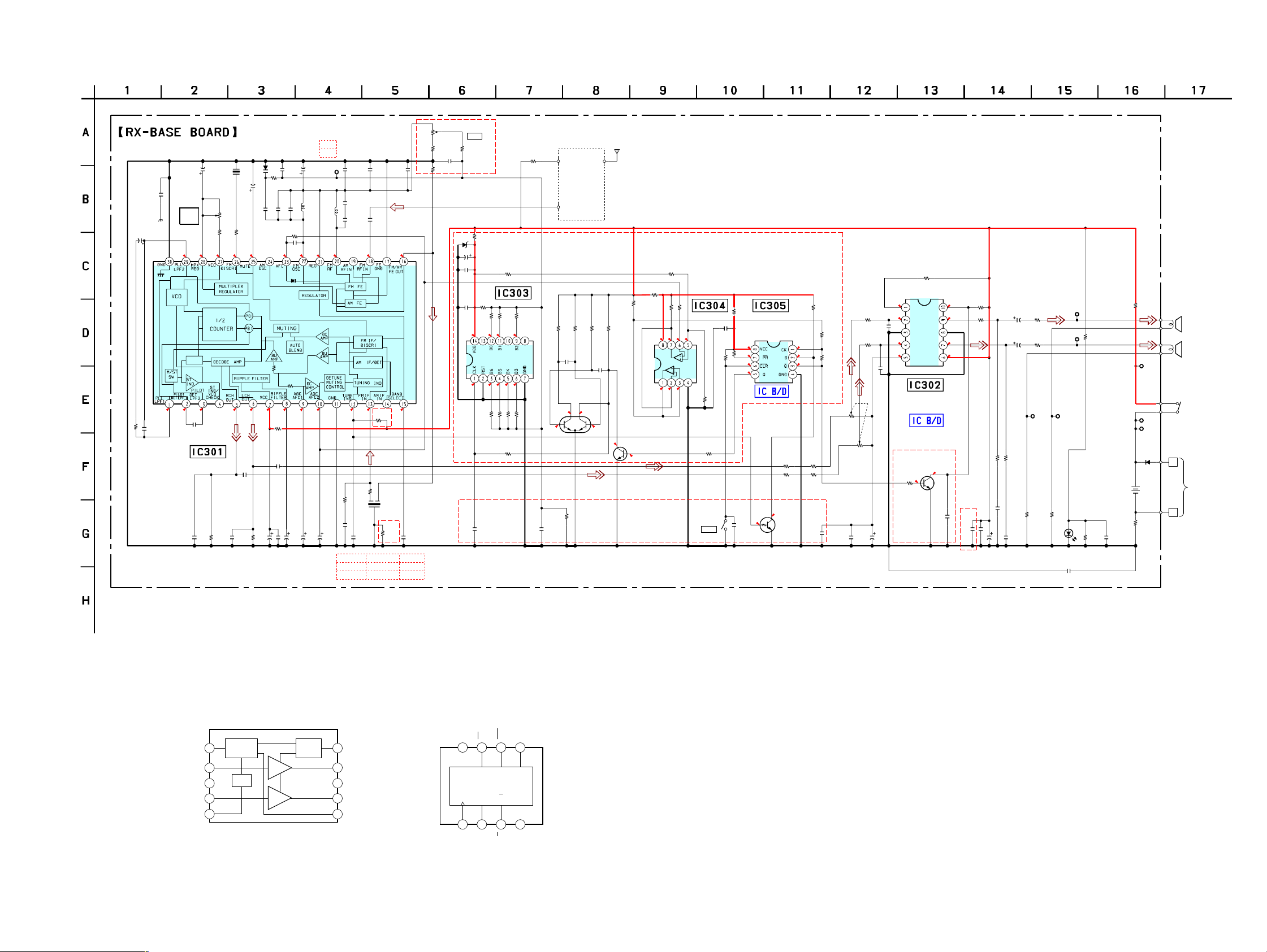
4-2. SCHEMATIC DIAGRAM
C311
10
16V
C366
C303
4.7/16V
R302
2.2k
0.001
CXA1538N-T4
IC301
C302
0.47
0.9
C304
0.022
FREE
RUN
FREQ.
0.9
0.8
C301
IF AMP/DET
RV301
4.7k
R310
3.3k
1.6
0.9
1
R304
3.3k
CF302
10.7MHz
DISC
1.3
C305
0.022
MDR-RF915R/RF845R
RF915R
RV303
R308
C334
10k
TUNE
JC324
1
2.2k
R366
150
D303
UDZ 2.2B
C347
47
16V
C346
0.22
C340
R340
0.1
4.7k
R341
470k
2.0
2.0
IC303
TC74HC4024
0
2.0
RF945R
C337
100p
JC304
COUNTER
R342
240k
2.0
0
7.5k
R347
R348
47k
2.0
15k
R346
R320
10
FE UNIT
(FRONT END)
0
R343
0
2.0
30k
R345
120k
62k
R344
R350
R351
15k
C342
0.01
Q301
FMW1-T-148
OSC
0
0.5
R349
10k
C341
0.1
C333
*
RF915R
D301
HVU363ATRU
C312
3.3
50V
JC311
0
1.0
1.6
0.7
0.7
C351
1
R305
3.3k
C306
C320
0.1
R312
15k
68p
10p
C315
C314
0.01
C313
R309
100k
0
2.1
2.3
R330
10
C350
1
C308
22
16V
C307
0.01
5p
RF945R
3p
C316
10
16V
L301
AIR COIL
C333
*
0
0
1.2
1.2
22
16V
C310
C309
*
C317
C352
0.001
0.001
C336
56p
µH
C332
0.33
L302
0
*
1
50V
150
R326
0.01
C335
RF915R
RF945R
C319
56p
0.01
0
R331
0
2.2k
1.3
RF945R
R325
330
10.7MHz
RF945R
C331
*
C309
2.2 50V
1 50V
CF301
JC302
R323
4.7k
C355
0.001
0
1.3
C329
0
0.01
C331
0.01
1
FM
(ANTENNA)
RF945R
R356
22k
JC303
0
R367
JC306
47k
0
R352
R353
1M
15k
1M
C343
0.01
IC304
0
0.4
0
0.6
2SC2712L
OSC SWITCH
2.4
BA10393F
0.9
Q303
22k
47k
ERROR AMP
R358
R355
1.2
1.0
0
0
R357
0.9
22k
R354
S301
TUNE
R332
1.0k
FF
C345
0.1
IC305
2.3
2.3
2.4
2.3
C344
0.1
0
TC7W74FU
Q305
DTC114TK
BUFFER
JC301
JC305
2.3
R361
22k
22k
R360
22k
R364
22k
R362
10k
0.6
2.3
R363
22k
0
RV302(1/2)
R327
33k
0
R328
0
33k
C367
0.001
(VOLUME)
C364
0.001
RV302(2/2)
C330
2.4
R333
2.2k
1.1
C361
100p
R334
2.2k
0
1.1
C362
100p
AUDIO AMP
IC302
LA4533MTP-1
RF945R
Q304
2SC2712L
AUDIO MUTE
33
16V
R318
2.3
0.1
47k
C323
0.1
R314
100k
2.3
1.1
JC309
0
1.1
2.4
RF915R
0.01
C345
0.01
C357
C324
6.3V
C325
JC331
220
0
6.3V
C326
JC332
220
0
6.3V
R316
10
10
R315
0.1
C327
JC334
JC333
0
0
C328
0.1
220
SLR-342VCTB7
D304
(power)
C365
0.001
RECHARGEABLE
(NICKEL-CADMIUM)
R321
1.5k
BATTERY
NC-AA
2pcs,2.4V
R322
6.8k
C363
0.01
JC336
JC335
0
0
D310
RB411D
N1-CD
+
-
+
-
+
-
SPEAKER
(L-ch)
SPEAKER
(R-ch)
S1
(POWER ON/OFF)
TO
TMR-RF915R/RF945R
(BATTERY
CHARGE
TERMINAL)
• IC BLOCK DIAGRAMS
IC302 LA4533MTP-1
POWER
1
P/SW
IN1
PRE GND
IN2
REF
SWITCH
2
3
4
AMP1
BIAS
AMP2
5
MUTE
CIRCIUT
10
MT/SW
OUT1
9
8
POWER GND
7
OUT2
6
VCC
IC305 TC7W74FU
CLR
PR
VCC
8
1
CK
6
7
RSQ
QDC
3Q2
D
Note on schematic diagrams.
Note:
• All capacitors are in µF unless otherwise noted. pF: µµF 50 WV or
less are not indicated except for electrolytics and tantalums.
• All resistors are in Ω and 1/
• A : B+ Line.
• H : adjustment for repair.
• Power voltage is dc 2.4V and fed with regulated dc power supply
Q
5
from battery terminal.
• Voltages are dc with respect to ground under no-signal conditions.
• Voltages are taken with a VOM (Input impedance 10 MΩ).
• Signal path.
F : FM
L : AUDIO
4
GND
9
9
4
W or less unless otherwise specified.
Loading...