


Ordering number : ENN*6696
CMOS IC
LC863364/56/48/40A
8-Bit Single Chip Microcontroller
Preliminary
Overview
The LC863364/56/48/40A are 8-bit single chip microcontrollers with the following on-chip functional blocks:
-CPU : Operable at a minimum bus cycle time of 0.424µ s
-On-chip ROM capacity
Program ROM : 64K/56K/48K/40K bytes
CGROM : 16K bytes
-On-chip RAM capacity : 640 bytes
-OSD RAM : 352 × 9 bits
-Five channels × 8-bit AD Converter
-Three channels × 7-bit PWM
-Two 16-bit timer/counters, 14-bit base timer
-8-bit synchronous serial interface circuit
-IIC-bus compliant serial interface circuit (Multi-master type)
-ROM correction function
-15-source 9-vectored interrupt system
-Integrated system clock generator and display clock generator
X’tal oscillator (32.768kHz) for PLL reference is used for TV control.
All of the above functions are fabricated on a single chip
|
|
|
|
|
|
|
|
|
|
|
|
|
|
|
|
|
|
|
|
|
|
|
|
|
|
|
|
|
|
|
|
|
|
|
|
|
|
|
|
|
|
|
|
|
|
|
|
|
|
|
|
|
|
|
|
|
|
|
|
|
|
|
|
|
|
|
|
|
|
|
|
|
|
|
|
|
|
|
|
|
|
|
|
|
|
|
|
|
|
|
|
|
|
|
|
|
|
|
|
|
|
|
|
|
|
|
|
|
|
|
|
|
|
|
|
|
|
|
|
|
|
|
|
|
|
|
|
|
|
|
|
|
|
|
|
|
|
|
|
|
|
|
|
|
|
|
|
|
|
|
|
|
|
|
|
|
|
|
|
|
|
|
|
|
|
|
|
|
|
|
|
|
|
|
|
|
|
|
|
|
|
|
|
|
|
|
|
|
|
|
|
|
|
|
|
|
|
|
|
|
|
|
|
|
|
|
|
|
|
|
|
|
|
|
|
|
|
|
|
|
|
|
|
|
|
|
|
|
|
|
|
|
|
|
|
|
|
|
|
|
|
|
|
|
|
|
|
|
|
|
|
|
|
|
|
|
|
|
|
|
|
|
|
|
|
|
|
|
|
|
|
|
|
|
|
|
|
|
|
|
|
|
|
|
|
|
|
|
|
|
|
|
|
|
|
|
|
|
|
|
|
|
|
|
|
|
|
|
|
|
|
|
|
|
|
|
|
|
|
|
|
|
|
|
|
|
|
|
|
|
|
|
|
|
|
|
|
|
|
|
|
|
|
|
|
|
|
|
|
|
|
|
|
|
|
|
|
|
|
|
|
|
|
|
|
|
|
|
|
|
|
|
|
|
|
|
|
|
|
|
|
|
|
|
|
|
|
|
|
|
|
|
|
|
|
|
|
|
|
|
|
|
|
|
|
|
|
|
|
|
|
|
|
|
|
|
|
|
|
|
|
|
|
|
|
|
|
|
|
|
|
|
|
|
|
|
|
|
|
|
|
|
|
|
|
|
|
|
|
|
|
|
|
|
|
|
|
|
|
|
|
|
|
|
|
|
|
|
|
|
|
|
|
|
|
|
|
|
|
|
|
|
|
|
|
|
|
|
|
|
|
|
|
|
|
|
|
|
|
|
|
|
|
|
|
|
|
|
|
|
|
|
|
|
|
|
|
|
|
|
|
|
|
|
|
|
|
|
|
|
|
|
|
|
|
|
|
|
|
|
|
|
|
|
|
|
|
|
|
|
|
|
|
|
|
|
|
|
|
|
|
|
|
|
|
|
|
|
|
|
|
|
|
|
|
|
|
|
|
|
|
|
|
|
|
|
|
|
|
|
|
|
|
|
|
|
|
|
|
|
|
|
|
|
|
|
|
|
|
|
|
|
|
|
|
|
|
|
|
|
|
|
|
|
|
|
|
|
|
|
|
|
|
|
|
|
|
|
|
|
|
|
|
|
|
|
|
|
|
|
|
|
|
|
|
|
|
|
|
|
|
|
|
|
|
|
|
|
|
|
|
|
|
|
|
|
|
|
|
|
|
|
|
|
|
|
|
|
|
|
|
|
|
|
|
|
|
|
|
|
|
|
|
|
|
|
|
|
|
|
|
|
|
|
|
|
|
|
|
|
|
|
|
|
|
|
|
|
|
|
|
|
|
|
|
|
|
|
|
|
|
|
|
|
|
|
|
|
|
|
|
|
|
|
|
|
|
|
|
|
|
|
|
|
|
|
|
|
|
|
|
|
|
|
|
|
|
|
|
|
|
|
|
|
|
|
|
|
|
|
|
|
|
|
|
|
|
|
|
|
|
|
|
|
|
|
|
|
|
|
|
|
|
|
|
|
|
|
|
|
|
|
|
|
|
|
|
|
|
|
|
|
|
|
|
|
|
|
|
|
|
|
|
|
|
|
|
|
|
|
|
|
|
|
|
|
|
|
|
|
|
|
|
|
|
|
|
|
|
|
|
|
|
|
|
|
|
|
|
|
|
|
|
|
|
|
|
|
|
|
|
|
|
|
|
|
|
|
|
|
|
|
|
|
|
|
|
|
|
|
|
|
|
|
|
|
|
|
|
|
|
|
|
|
|
|
|
|
|
|
|
|
|
|
|
|
|
|
|
|
|
|
|
|
|
|
|
|
|
|
|
|
|
|
|
|
|
|
|
|
|
|
|
|
|
|
|
|
|
|
|
|
|
|
|
|
|
|
|
|
|
|
|
|
|
|
|
|
|
|
|
|
|
|
|
|
|
|
|
|
|
|
|
|
|
|
|
|
|
|
|
|
|
|
|
|
|
|
|
|
|
|
|
|
|
|
|
|
|
|
|
|
|
|
|
|
|
|
|
|
|
|
|
|
|
|
|
|
|
|
|
|
|
|
|
|
|
|
|
|
|
|
|
|
|
|
|
|
|
|
|
|
|
|
|
|
|
|
|
|
|
|
|
|
|
|
|
|
|
|
|
|
|
|
|
|
|
|
|
|
|
|
|
|
|
|
|
|
|
|
|
|
|
|
|
|
|
|
|
|
|
|
|
|
|
|
|
|
|
|
|
|
|
|
|
|
|
|
|
|
|
|
|
|
|
|
|
|
|
|
|
|
|
|
|
|
|
|
|
|
|
|
|
|
|
|
|
|
|
|
|
|
|
|
|
|
|
|
|
|
|
|
|
|
|
|
|
|
|
|
|
|
|
|
|
|
|
|
|
|
|
|
|
|
|
|
|
|
|
|
|
|
|
|
|
|
|
|
|
|
|
|
|
|
|
|
|
|
|
|
|
|
|
|
|
|
|
|
|
|
|
|
|
|
|
|
|
|
|
|
|
|
|
|
|
|
|
|
|
|
|
|
|
|
|
|
|
|
|
|
|
|
|
|
|
|
|
|
|
|
|
|
|
|
|
|
|
|
|
|
|
|
|
|
|
|
|
|
|
|
|
|
|
|
|
|
|
|
|
|
|
|
|
|
|
|
|
|
|
|
|
|
|
|
|
|
|
|
|
|
|
|
|
|
|
|
|
|
|
|
|
|
|
|
|
|
|
|
|
|
|
|
|
|
|
|
|
|
|
|
|
|
|
|
|
|
|
|
|
|
|
|
|
|
|
|
|
|
|
|
|
|
|
|
|
|
|
|
|
|
|
|
|
|
|
|
|
|
|
|
|
|
|
|
|
|
|
|
|
|
|
|
|
|
|
|
|
|
|
|
|
|
|
|
|
|
|
|
|
|
|
|
|
|
|
|
|
|
|
|
|
|
|
|
|
|
|
|
|
|
|
|
|
|
|
|
|
|
|
|
|
|
|
|
|
|
|
|
|
|
|
|
|
|
|
|
|
|
|
|
|
|
|
|
|
|
|
|
|
|
|
|
|
|
|
|
|
|
|
|
|
|
|
|
|
|
|
|
|
|
|
|
|
|
|
|
|
|
|
|
|
|
|
|
|
|
|
|
|
|
|
|
|
|
|
|
|
|
|
|
|
|
|
|
|
|
|
|
|
|
|
|
|
|
|
|
|
|
|
|
|
|
|
|
|
|
|
|
|
|
|
|
|
|
|
|
|
|
|
|
|
|
|
|
|
|
|
|
|
|
|
|
|
|
|
|
|
|
|
|
|
|
|
|
|
|
|
|
|
|
|
|
|
|
|
|
|
|
|
|
|
|
|
|
|
|
|
|
|
|
|
|
|
|
|
|
|
|
|
|
|
|
|
|
|
|
|
|
|
|
|
|
|
|
|
|
|
|
|
|
|
|
|
|
|
|
|
|
|
|
|
|
|
|
|
|
|
|
|
|
|
|
|
|
|
|
|
|
|
|
|
|
|
|
|
|
|
|
|
|
|
|
|
|
|
|
|
|
|
|
|
|
|
|
|
|
|
|
|
|
|
|
|
|
|
|
|
|
|
|
|
|
|
|
|
|
|
|
|
|
|
|
|
|
|
|
|
|
|
|
|
|
|
|
|
|
|
|
|
|
|
|
|
|
|
|
|
|
|
|
|
|
|
|
|
|
|
|
|
|
|
|
|
|
|
|
|
|
|
|
|
|
|
|
|
|
|
|
|
|
|
|
|
|
|
|
|
|
|
|
|
|
|
|
|
|
|
|
|
|
|
|
|
|
|
|
|
|
|
|
|
|
|
|
|
|
|
|
|
|
|
|
|
|
|
|
|
|
|
|
|
|
|
|
|
|
|
|
|
|
|
|
|
|
|
|
|
|
|
|
|
|
|
|
|
|
|
|
|
|
|
|
|
|
|
|
|
|
|
|
|
|
|
|
|
|
|
|
|
|
|
|
|
|
|
|
|
|
|
|
|
|
|
|
|
|
|
|
|
|
|
|
|
|
|
|
|
|
|
|
|
|
|
|
|
|
|
|
|
|
|
|
|
|
|
|
|
|
|
|
|
|
|
|
|
|
|
|
|
|
|
|
|
|
|
|
|
|
|
|
|
|
|
|
|
|
|
|
|
|
|
|
|
|
|
|
|
|
|
|
|
|
|
|
|
|
|
Ver.0.91 |
|
|
|
|
|
|
|
|
|
|
|
|
|
|
|
|
|
|
|
|
|
|
|
|
|
|
|
|
|
|
|
|
|
|
|
|
|
|
|
|
|
|
|
|
|
|
|
|
|
|
|
|
|
|
|
|
|
|
|
|
|
|
|
|
|
|
|
|
|
|
|
|
|
|
|
|
|
|
|
|
|
|
|
|
|
|
|
|
|
|
|
|
|
|
|
|
|
|
|
|
|
|
|
|
|
|
|
|
|
|
|
|
|
|
|
|
|
|
|
|
|
|
|
|
|
|
91400 RM (IM) HS No.6696-1/20 |
||||||||||||||||||||||||||||||||||||||||||||||||||||||||||||||||||||||||||||||||||||||||||||||
|
|
|
|
|
|
|
|
|
|
|
|
|
|
|
|
|
|
|
|
|
|
|
|
|
|
|
|
|
|
|
|
|
|
|
|
|
|
|
|
|
|
|
|
|
|
|
|
|
|
|
|
|
|
|
|
|
|
|
|
|
|
|
|
|
|
|
|
|
|
|
|
|
|
|
|
|
|
|
|
|
|
|
|
|
|
|
|
|
|
|
|
|
|
|
|
|
|
|
|
|
|
|
|
|
|
|
|
|
|
|
|
|
|
|
|
|
|
|
|
|
|
|
|
|
|
||||||||||||||||||||||||||||||||||||||||||||||||||||||||||||||||||||||||||||||||||||||||||||||||
|
|
|
|
|
|
|
|
|
|
|
|
|
|
|
|
|
|
|
|
|
|
|
|
|
|
|
|
|
|
|
|
|
|
|
|
|
|
|
|
|
|
|
|
|
|
|
|
|
|
|
|
|
|
|
|
|
|
|
|
|
|
|
|
|
|
|
|
|
|
|
|
|
|
|
|
|
|
|
|
|
|
|
|
|
|
|
|
|
|
|
|
|
|
|
|
|
|
|
|
|
|
|
|
|
|
|
|
|
|
|
|
|
|
|
|
|
|
|
|
|
|
|
|
|
|
||||||||||||||||||||||||||||||||||||||||||||||||||||||||||||||||||||||||||||||||||||||||||||||||
51299 |
|
|
|
|
|
|
|
|
|
|
|
|
|
|
|
|
|
|
|
|
|
|
|
|
|
|
|
|
|
|
|
|
|
|
|
|
|
|
|
|
|
|
|
|
|
|
|
|
|
|
|
|
|
|
|
|
|
|
|
|
|
|
|
|
|
|
|
|
|
|
|
|
|
|
|
|
|
|
|
|
|
|
|
|
|
|
|
|
|
|
|
|
|
|
|
|
|
|
|
|
|
|
|
|
|
|
|
|
|
|
|
|
|
|
|
|
|
|
|
|
|
|
|
|
|
|
|
|
|
|
|
|
|
|
|
|
|
|
|
|
|
|
|
|
|
|
|
|
|
|
|
|
|
|
|
|
|
|
|
|
|
|
|
|
|
|
|
|
|
|
|
|
|
|
|
|
|
|
|
|
|
|
|
|
|
|
|
|
|
|
|
|
|
|
|
|
|
|
|
|
|
|
|
|
|
|
|
|
|
|
|
|
|
|
|
|
|
|
|
|
|

LC863364/56/48/40A
Features
(1) Read-Only Memory (ROM) : 65024 × 8 bits / 57344 × 8 bits / 49152 × 8 bits 40960 × 8 bits for program
16128 × 8 bits for CGROM
(2) Random Access Memory (RAM) : 640 × 8 bits (including 128 bytes for ROM correction function) 352 × 9 bits (for CRT display)
(3) OSD functions |
|
|
- Screen display |
: 36 characters × 16 lines (by software) |
|
- RAM |
: 352 words (9 bits per word) |
|
Display area |
: 36 words × |
8 lines |
Control area |
: 8 words × |
8 lines |
- Characters |
|
|
Up to 252 kinds of 16 × 32 dot character fonts |
||
|
(4 characters including 1 test character are not programmable) |
|
Each font can be divided into two parts and used as two fonts : |
||
|
a 16 × 17 dot and 8 × 9 dot character font |
|
- Various character attributes |
|
|
Character colors |
|
: 16 colors |
Character background colors |
: 16 colors |
|
Fringe / shadow colors |
: 16 colors |
|
Full screen colors |
: 16colors |
|
Rounding |
|
|
Underline |
|
|
Italic character (slanting) |
|
|
-Attribute can be changed without spacing
-Vertical display start line number can be set for each row independently (Rows can be overlapped)
-Horizontal display start position can be set for each row independently
-Horizontal pitch (bit 9 - 16)*1 and vertical pitch (bit-32) can be set for each row independently
-Different display modes can be set for each row independently
Caption |
• Text mode / OSD mode 1 / OSD mode 2 (Quarter size) / Simplifed graphic mode |
- Ten character sizes *1 |
|
Horez. × |
Vert. = (1 × 1), (1 × 2), (2 × 2), (2 × 4), (0.5 × 0.5) |
|
(1.5 × 1), (1.5 × 2), (3 × 2), (3 × 4), (0.75 × 0.5) |
-Shuttering and scrolling on each row
-Simplified Graphic Display
*1 Note : range depends on display mode : refer to the manual for details.
(4) Bus Cycle Time / Instruction-Cycle Time
Bus cycle time |
|
Instruction cycle time |
System clock oscillation |
|
Oscillation Frequency |
Voltage |
||
0.424µ |
s |
|
0.848µ s |
|
Internal VCO |
|
14.156MHz |
4.5V to 5.5V |
|
|
|
|
(Ref : X’tal 32.768kHz) |
|
|
|
|
7.5µ s |
|
|
15.0µ s |
|
Internal RC |
|
800kHz |
4.5V to 5.5V |
183.1µ |
s |
|
366.2µ s |
|
Crystal |
|
32.768kHz |
4.5V to 5.5V |
(5) Ports |
|
|
|
|
|
|
|
|
- Input / Output Ports |
|
|
: 5 ports (28 terminals) |
|
||||
Data direction programmable in nibble units |
|
: 1 port (8 terminals) |
|
|
||||
(If the N-ch open drain output is selected by option, the corresponding port data can be read in output mode.) |
|
|||||||
Data direction programmable for each bit individually |
: 4 ports (20 terminals) |
|
||||||
- Input port |
|
|
: 1 port (1 terminal) |
|
|
|||
No.6696-2/20

LC863364/56/48/40A
(6)AD converter
-5 channels × 8-bit AD converters
(7)Serial interfaces
-IIC-bus compliant serial interface (Multi-master type)
Consists of a single built-in circuit with two I/O channels. The two data lines and two clock lines can be connected internally.
-Synchronous 8-bit serial interface
(8)PWM output
-3 channels × 7-bit PWM
(9)Timer
-Timer 0 : 16-bit timer/counter
With 2-bit prescaler + 8-bit programmable prescaler
Mode 0 : Two 8-bit timers with a programmable prescaler
Mode 1 : 8-bit timer with a programmable prescaler + 8-bit counter
Mode 2 : 16-bit timer with a programmable prescaler
Mode 3 : 16-bit counter
The resolution of timer is 1 tCYC.
-Timer 1 : 16-bit timer/PWM Mode 0 : Two 8-bit timers
Mode 1 : 8-bit timer + 8-bit PWM Mode 2 : 16-bit timer
Mode 3 : Variable bit PWM (9 to 16 bits)
In mode0/1,the resolution of Timer1/PWM is 1 tCYC
In mode2/3,the resolution is selectable by program; tCYC or 1/2 tCYC
-Base timer
Generate every 500ms overflow for a clock application (using 32.768kHz crystal oscillation for the base timer clock) Generate every 976µ s, 3.9ms, 15.6ms, 62.5ms overflow (using 32.768kHz crystal oscillation for the base timer clock)
Clock for the base timer is selectable from 32.768kHz crystal oscillation, system clock or programmable prescaler output of Timer 0
(10)Remote control receiver circuit (connected to the P73/INT3/T0IN terminal)
-Noise rejection function
-Polarity switching
(11)Watchdog timer
External RC circuit is required
Interrupt or system reset is activated when the timer overflows
(12)ROM correction function Max 128 bytes / 2 addresses
(13)Interrupts
-15 sources 9 vectored interrupts
1.External Interrupt INT0
2.External Interrupt INT1
3.External Interrupt INT2, Timer/counter T0L (Lower 8 bits)
4.External Interrupt INT3, base timer
5.Timer/counter T0H (Upper 8 bits)
6.Timer T1H,T1L
7.SIO0
8.Vertical synchronous signal interrupt ( VS ), horizontal line ( HS ), AD
9.IIC, Port 0
No.6696-3/20

LC863364/56/48/40A
- Interrupt priority control
Three interrupt priorities are supported (low, high and highest) and multi-level nesting is possible. Low or high priority can be assigned to the interrupts from 3 to 9 listed above. For the external interrupt INT0 and INT1, high or highest priority can be set.
(14)Sub-routine stack level
-A maximum of 128 levels (stack is built in the internal RAM)
(15)Multiplication/division instruction
-16 bits × 8 bits (7 instruction cycle times)
-16 bits / 8 bits (7 instruction cycle times)
(16)3 oscillation circuits
-Built-in RC oscillation circuit used for the system clock
-Built-in VCO circuit used for the system clock and OSD
-X’tal oscillation circuit used for base timer, system clock and PLL reference
(17)Standby function
-HALT mode
The HALT mode is used to reduce the power dissipation. In this operation mode, the program execution is stopped. This mode can be released by the interrupt request or the system reset.
- HOLD mode
The HOLD mode is used to stop the oscillations; RC (internal), VCO, and X’tal oscillations. This mode can be released by the following conditions.
•Pull the reset terminal ( RES ) to low level.
•Feed the selected level to either P70/INT0 or P71/INT1.
•Input the interrupt condition to Port 0.
(18)Package
-DIP42S
-QIP48E
(19)Development tools
- Flash EEPROM: |
2 Flash microcontrollers are available:LC86F3364A,LC86F3348A. Flash version is different on |
|
which microcontroller is used. |
|
LC86F3364A (LC863364A / LC863356A) (under development) |
|
LC86F3348A (LC863348A / LC863340A) |
- Evaluation chip: |
LC863096 |
- Emulator: |
EVA86000 (main) + ECB863200 (evaluation chip board) |
|
+ POD863300 (pod: DIP42S) or POD863301 (QIP48E) |
No.6696-4/20
LC863364/56/48/40A
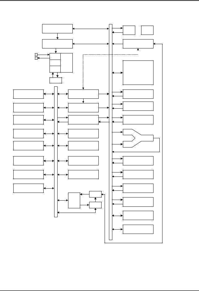
System Block Diagram
Interrupt Control |
|
|
IR |
PLA |
|
|
|
|
|
||
Standby Control |
|
|
|
ROM |
|
X’tal |
Clock Generator |
|
|
|
|
RC |
|
|
|
|
|
|
|
|
|
|
|
VCO |
|
|
|
|
PC |
|
|
|
|
|
|
PLL |
|
|
|
|
|
IIC |
|
ROM Correct Control |
|
ACC |
|
SIO0 |
|
XRAM |
|
|
B Register |
|
|
|
|
||
Timer 0 |
|
Bus Interface |
|
C Register |
|
Timer 1 |
|
Port 1 |
|
|
|
|
|
|
|
|
ALU |
Base Timer |
|
Port 6 |
|
|
|
ADC |
|
Port 7 |
|
|
PSW |
INT0-3 |
|
Port 8 |
|
|
RAR |
Noise Rejection Filter |
|
|
|
||
|
|
|
|
|
|
PWM |
|
|
|
|
RAM |
|
|
OSD |
CGROM |
|
|
|
|
|
|
|
|
|
|
Control |
|
Stack Pointer |
|
|
|
Circuit |
VRAM |
||
|
|
|
|
||
|
|
|
|
|
|
|
|
|
|
|
Port 0 |
|
|
|
|
Watch Dog Timer |
|
No.6696-5/20
LC863364/56/48/40A
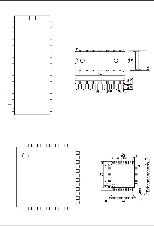
Pin Assignment
• DIP42S
P10/SO0 |
1 |
42 |
P07 |
|
|
P11/SI0 |
2 |
41 |
P06 |
|
|
P12/SCK0 |
3 |
40 |
P05 |
|
|
P13/PWM1 |
4 |
39 |
P04 |
Package Dimension |
|
P14/PWM2 |
5 |
38 |
P03 |
||
P15/PWM3 |
6 |
37 |
P02 |
(unit : mm) |
|
3025B |
|||||
P16 |
7 |
36 |
P01 |
||
|
|||||
P17/PWM |
8 |
35 |
P00 |
|
|
VSS |
9 |
34 |
P73/INT3/T0IN |
|
|
XT1 |
10 |
33 |
P72/INT2/T0IN |
|
|
XT2 |
11 |
32 |
P71/INT1 |
|
|
VDD |
12 |
31 |
P70/INT0 |
|
|
P84/AN4 |
13 |
30 |
P63/SCLK1 |
|
|
P85/AN5 |
14 |
29 |
P62/SDA1 |
|
|
P86/AN6 |
15 |
28 |
P61/SCLK0 |
|
|
P87/AN7 |
16 |
27 |
P60/SDA0 |
|
|
RES |
17 |
26 |
I |
SANYO : DIP-42S(600mil) |
|
FILT |
18 |
25 |
BL |
||
P83/AN3 |
19 |
24 |
B |
|
|
VS |
20 |
23 |
G |
|
|
HS |
21 |
22 |
R |
|
• QIP48E
|
|
|
NC |
|
|
|
|
|
|
|
|
|
48 |
||
P15/PWM3 |
|
1 |
|
|
|
||
P16 |
|
2 |
|
|
|
||
P17/PWM |
|
3 |
|
|
|
||
VSS |
|
4 |
|
|
|
||
XT1 |
|
5 |
|
|
|
||
XT2 |
|
6 |
|
|
|
||
VDD |
|
7 |
|
|
|
||
NC |
|
8 |
|
|
|
||
P84/AN4 |
|
9 |
|
|
|
||
P85/AN5 |
|
10 |
|
|
|||
P86/AN6 |
|
11 |
|
|
|||
P87/AN7 |
|
12 |
|
|
|||
|
|
13 |
|
|
|
||
|
|
|
|
|
|
|
|
|
|
|
RES |
|
|
|
|
P14/PWM2 |
|
P13/PWM1 |
|
P12/SCK0 |
|
P11/SI0 |
|
P10/SO0 |
|
NC |
|
P07 |
|
P06 |
|
P05 |
|
P04 |
|
P03 |
Package Dimension |
|
|
|
|
|
|
|
|
|
|
|
|
|
|
|
|
|
|
|
|
|
|
|
|
|
|
|
|
|
|
|
|
|
|
|
|
|
|
|
|
|
|
|
47 |
46 |
45 |
44 |
43 |
42 |
41 |
40 |
39 |
38 |
37 |
|
(unit : mm) |
|
3156 |
|||||||||||
|
|
|
|
|
|
|
|
|
|
36 |
P02 |
|
|
|
|
|
|
|
|
|
|
|
|
||
|
|
|
|
|
|
|
|
|
|
35 |
P01 |
|
|
|
|
|
|
|
|
|
|
|
34 |
P00 |
|
|
|
|
|
|
|
|
|
|
|
33 |
NC |
|
|
|
|
|
|
|
|
|
|
|
32 |
P73/INT3/T0IN |
|
|
|
|
|
|
|
|
|
|
|
31 |
P72/INT2/T0IN |
|
|
|
|
|
|
|
|
|
|
|
30 |
P71/INT1 |
|
|
|
|
|
|
|
|
|
|
|
29 |
P70/INT0 |
|
|
|
|
|
|
|
|
|
|
|
28 |
P63/SCLK1 |
|
|
|
|
|
|
|
|
|
|
|
27 |
P62/SDA1 |
|
|
|
|
|
|
|
|
|
|
|
26 |
P61/SCLK0 |
|
|
|
|
|
|
|
|
|
|
|
25 |
P60/SDA0 |
|
14 |
15 |
16 |
17 |
18 |
19 |
20 |
21 |
22 |
23 |
24 |
|
|
FILT |
P83/AN3 |
NC |
VS |
HS |
R |
G |
B |
BL |
I |
NC |
|
SANYO : QIP-48E |
|
|
|||||||||||
|
|
|
|
|
|
|
|
|
|
|
|
No.6696-6/20 |
 Loading...