


Ordering number : EN4828A
CMOS LSI
LC75852E, 75852W
Asynchronous Silicon Gate 1/2 Duty LCD Driver with On-Chip Key Input Function
Overview
The LC75852E and LC75852W are 1/2 duty dynamic LCD display drivers. In addition to being able to directly drive LCD panels with up to 90 segments, they can also control up to four general-purpose output ports. These products also include a key scan circuit which allows them to accept input from keypads with up to 30 keys. This allows end product front panel wiring to be simplified.
Features
•Up to 30 key inputs (Key scan is only performed when a key is pressed.)
•1/2 duty – 1/2 bias (up to 90 segments)
•Sleep mode and the all segments off function can be controlled from serial data.
•Segment output port/general-purpose output port usage can be controlled from serial data.
•Serial data I/O supports CCB format communication with the system controller.
•High generality since display data is displayed directly without decoder intervention
•Reset pin that can establish the initial state.
•CCB is a trademark of SANYO ELECTRIC CO., LTD.
•CCB is SANYO’s original bus format and all the bus addresses are controlled by SANYO.
Specifications
Absolute Maximum Ratings at Ta = 25°C, VSS = 0 V
Package Dimensions
unit: mm
3159-QFP64E
[LC75852E]
SANYO: QIP64E
unit: mm
3190-SQFP64
[LC75852W]
SANYO: SQFP64
Parameter |
Symbol |
|
|
Conditions |
Ratings |
Unit |
|
|
|
|
|
|
|
Maximum supply voltage |
VDD max |
VDD |
–0.3 to +7.0 |
V |
||
Input voltage |
VIN |
|
|
|
||
OSC, CE, CL, DI, |
RES, |
KI1 to KI5 |
–0.3 to VDD + 0.3 |
V |
||
Output voltage |
VOUT |
OSC, DO, S1 to S45, COM1, COM2, KS1 to KS6, P1 to P4 |
–0.3 to VDD + 0.3 |
V |
||
|
IOUT1 |
S1 to S45 |
100 |
µA |
||
Output current |
IOUT2 |
COM1, COM2, KS1 to KS6 |
1 |
mA |
||
|
IOUT3 |
P1 to P4 |
5 |
mA |
||
Allowable power dissipation |
Pd max |
Ta = 85°C |
200 |
mW |
||
|
|
|
|
|
|
|
Operating temperature |
Topr |
|
|
|
–40 to +85 |
°C |
|
|
|
|
|
|
|
Storage temperature |
Tstg |
|
|
|
–55 to +125 |
°C |
SANYO Electric Co.,Ltd. Semiconductor Bussiness Headquarters
TOKYO OFFICE Tokyo Bldg., 1-10, 1 Chome, Ueno, Taito-ku, TOKYO, 110 JAPAN
63096HA (OT)/N1594TH (OT) B8-1326, 1328 No. 4828-1/16

LC75852E, 75852W
Allowable Operating Ranges at Ta = –40 to +85°C, VSS = 0 V
|
|
Parameter |
Symbol |
|
|
|
|
Conditions |
min |
typ |
max |
Unit |
|
|
|
|
|
|
|
|
|
|
|
|
|
|
Supply voltage |
VDD |
VDD |
4.5 |
|
6.0 |
V |
|||||
|
|
|
VIH1 |
|
|
|
|
|
|
|
||
|
Input high-level voltage |
CE, CL, DI, |
RES |
|
0.8 VDD |
|
VDD |
V |
||||
|
VIH2 |
KI1 to KI5 |
0.6 VDD |
|
VDD |
V |
||||||
|
|
|
|
|||||||||
|
Input low-level voltage |
VIL |
|
|
|
|
|
|
|
|||
|
CE, CL, DI, |
RES, |
KI1 to KI5 |
0 |
|
0.2 VDD |
V |
|||||
|
Recommended external |
ROSC |
OSC |
|
62 |
|
kΩ |
|||||
|
resistance |
|
|
|||||||||
|
|
|
|
|
|
|
|
|
|
|
||
|
|
|
|
|
|
|
|
|
|
|
|
|
|
Recommended external |
COSC |
OSC |
|
680 |
|
pF |
|||||
|
capacitance |
|
|
|||||||||
|
Guaranteed oscillator range |
fOSC |
OSC |
25 |
50 |
100 |
kHz |
|||||
|
Data setup time |
tds |
CL, DI: Figure 1 |
160 |
|
|
ns |
|||||
|
Data hold time |
tdh |
CL, DI: Figure 1 |
160 |
|
|
ns |
|||||
|
CE wait time |
tcp |
CE, CL: Figure 1 |
160 |
|
|
ns |
|||||
|
CE setup time |
tcs |
CE, CL: Figure 1 |
160 |
|
|
ns |
|||||
|
CE hold time |
tch |
CE, CL: Figure 1 |
160 |
|
|
ns |
|||||
|
High-level clock pulse width |
tøH |
CL: Figure 1 |
160 |
|
|
ns |
|||||
|
Low-level clock pulse width |
tøL |
CL: Figure 1 |
160 |
|
|
ns |
|||||
|
Rise time |
tr |
CE, CL, DI: Figure 1 |
|
160 |
|
ns |
|||||
|
Fall time |
tf |
CE, CL, DI: Figure 1 |
|
160 |
|
ns |
|||||
|
DO output delay time |
tdc |
DO, RPU = 4.7 kΩ , CL = 10 pF*: Figure 1 |
|
|
1.5 |
µs |
|||||
|
DO rise time |
tdr |
DO, RPU = 4.7 kΩ , CL = 10 pF*: Figure 1 |
|
|
1.5 |
µs |
|||||
|
|
switching time |
t2 |
Figure 2 |
10 |
|
|
µs |
||||
|
RES |
|
|
|||||||||
Note: * Since DO is an open-drain output, these values differ depending on the pull-up resistor RPU and the load capacitance CL. |
|
|
||||||||||
Electrical Characteristics in the Allowable Operating Ranges |
|
|
|
|
||||||||
|
|
|
|
|
|
|
|
|
|
|
|
|
|
|
Parameter |
Symbol |
|
|
|
|
Conditions |
min |
typ |
max |
Unit |
|
|
|
|
|
|
|
|
|
|
|
|
|
|
Hysteresis |
VH |
|
|
|
|
|
|
|
|||
|
CE, CL, DI, |
RES, |
KI1 to KI5 |
|
0.1 VDD |
|
V |
|||||
|
Input high-level current |
IIH |
|
|
|
|
|
|
|
|||
|
CE, CL, DI, RES: VI = 6.0 V |
|
|
5.0 |
µA |
|||||||
|
Input low-level current |
IIL |
|
|
|
|
|
|
|
|||
|
CE, CL, DI, RES: VI = 0 V |
–5.0 |
|
|
µA |
|||||||
|
Input floating voltage |
VIF |
KI1 to KI5 |
|
|
0.05 VDD |
V |
|||||
|
Pull-down resistance |
RPD |
KI1 to KI5: VDD = 5.0 V |
50 |
100 |
250 |
kΩ |
|||||
|
Output off leakage current |
IOFFH |
DO: VO = 6.0 V |
|
|
6.0 |
µA |
|||||
|
|
|
VOH1 |
KS1 to KS6: IO = –1 mA |
VDD – 1.0 |
|
|
V |
||||
|
Output high-level voltage |
VOH2 |
P1 to P4: IO = –1 mA |
VDD – 1.0 |
|
|
V |
|||||
|
VOH3 |
S1 to S45: IO = –10 µA |
VDD – 1.0 |
|
|
V |
||||||
|
|
|
|
|
||||||||
|
|
|
VOH4 |
COM1, COM2: IO = –100 µA |
VDD – 0.6 |
|
|
V |
||||
|
|
|
VOL1 |
KS1 to KS6: IO = 50 µA |
0.4 |
1.0 |
3.0 |
V |
||||
|
|
|
VOL2 |
P1 to P4: IO = 1 mA |
|
|
1.0 |
V |
||||
|
Output low-level voltage |
VOL3 |
S1 to S45: IO = 10 µA |
|
|
1.0 |
V |
|||||
|
|
|
VOL4 |
COM1, COM2: IO = 100 µA |
|
|
0.6 |
V |
||||
|
|
|
VOL5 |
DO: IO = 1 mA |
|
0.1 |
0.5 |
V |
||||
|
Output middle-level voltage |
VMID1 |
COM1, COM2: VDD = 6.0 V, IO = ±100 µA |
2.4 |
3.0 |
3.6 |
V |
|||||
|
VMID2 |
COM1, COM2: VDD = 4.5 V, IO = ±100 µA |
1.65 |
2.25 |
2.85 |
V |
||||||
|
|
|
||||||||||
|
Current drain |
IDD1 |
Sleep mode, Ta = 25°C |
|
|
5 |
µA |
|||||
|
IDD2 |
VDD = 6.0 V, output open, Ta = 25°C, fOSC = 50 kHz |
|
1.4 |
2.5 |
mA |
||||||
|
|
|
|
|||||||||
No. 4828-2/16

LC75852E, 75852W
1. When stopped with CL at the low level
2. When stopped with CL at the high level
Figure 1
Pin Assignment
No. 4828-3/16
LC75852E, 75852W
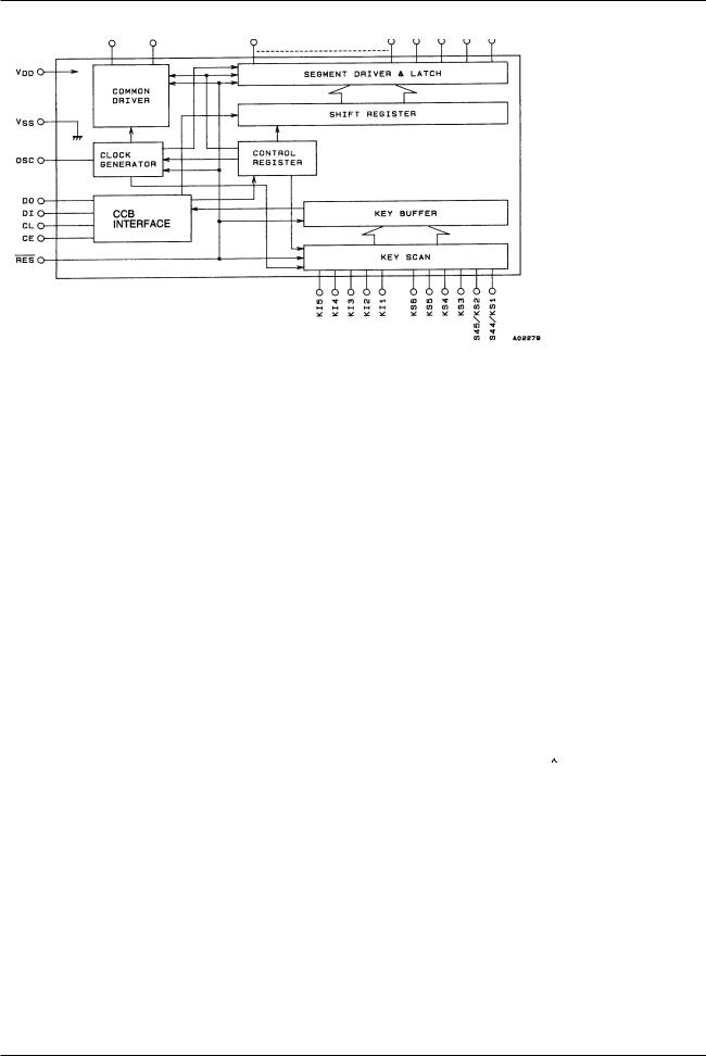
Block Diagram
Pin Functions
|
|
Pin |
Pin No. |
|
Function |
|
Active |
I/O |
Handling when |
|||
|
|
|
|
unused |
||||||||
|
|
|
|
|
|
|
|
|
|
|
|
|
|
|
|
|
|
|
|
|
|
|
|
||
S1/P1 to S4/P4 |
1 to 4 |
Segment outputs: Used to output the display data that is transmitted over the |
|
|
|
|
|
|
||||
serial data input. Pins S1/P1 to S4/P4 can be used as general-purpose outputs |
|
— |
O |
Open |
||||||||
S5 to S43 |
5 to 43 |
|
||||||||||
according to control data specification. |
|
|
|
|
|
|
||||||
|
|
|
|
|
|
|
|
|
|
|||
|
|
|
|
|
|
|
|
|
|
|
|
|
COM1 |
44 |
Common driver outputs. The frame frequency fO is (fOSC/512) Hz. |
|
— |
O |
Open |
||||||
COM2 |
45 |
|
||||||||||
|
|
|
|
|
|
|
|
|
||||
|
|
|
|
|
|
|
|
|
|
|
||
|
|
|
|
Key scan outputs. When a key matrix is formed, normally a diode will be |
|
|
|
|
|
|
||
KS1/S44, |
46 |
attached to the key scan timing line to prevent shorts. However, since the |
|
|
|
|
|
|
||||
KS2/S45, |
47 |
output transistor impedance is an unbalanced CMOS output, it will not be |
|
— |
O |
Open |
||||||
KS3 to KS6 |
48 to 51 |
damaged if shorted. Pins KS1/S44 and KS2/S45 can be used as segment |
|
|
|
|
|
|
||||
|
|
|
|
outputs according to control data specification. |
|
|
|
|
|
|
||
|
|
|
|
|
|
|
|
|
|
|
||
KI1 to KI5 |
52 to 56 |
Key scan inputs: Pins with a built-in pull-down resistor. |
|
H |
I |
GND |
||||||
|
|
|
|
|
|
|
|
|
|
|
||
OSC |
57 |
Oscillator connection: Oscillator circuit can be formed by connecting the pin to |
|
— |
I/O |
VDD |
||||||
a resistor and a capacitor. |
|
|
|
|||||||||
|
|
|
|
|
|
|
|
|
|
|
|
|
|
|
|
|
|
|
|
|
|
|
|
|
|
CE |
62 |
Serial data interface: Connected |
|
CE: Chip enable |
|
H |
I |
|
||||
CL |
63 |
|
|
|
|
|
|
GND |
||||
to the controller. Since DO is an |
|
CL: Synchronization clock |
|
|
|
|
I |
|||||
|
|
|
|
|
||||||||
DI |
64 |
open-drain output, it requires a |
|
DI: Transfer data |
|
— |
I |
|
||||
pull-up resistor. |
|
DO: Output data |
|
|
||||||||
|
|
|
|
|
|
|
|
|
|
|
||
DO |
61 |
|
|
|
|
— |
O |
Open |
||||
|
|
|
|
|
|
|
|
|
|
|
|
|
|
|
|
|
Reset input that re-initializes the LSI internal states. During a reset, the display |
|
|
|
|
|
|
||
|
|
|
|
segments are turned off forcibly regardless of the internal display data. All |
|
|
|
|
|
GND |
||
RES |
59 |
|
|
L |
I |
|||||||
internal key data is reset to low and the key scan operation is disabled. |
|
|
||||||||||
|
|
|
|
|
|
|
|
|
|
|||
|
|
|
|
However, serial data can be input during a reset. |
|
|
|
|
|
|
||
|
|
|
|
|
|
|
|
|
|
|
||
VDD |
60 |
Power supply connection. A supply voltage of between 4.5 and 6.0 V must be |
|
— |
— |
— |
||||||
provided. |
|
|
|
|||||||||
|
|
|
|
|
|
|
|
|
|
|
|
|
|
|
|
|
|
|
|
|
|
|
|
||
VSS |
58 |
Power supply ground connection. Must be connected to GND. |
|
— |
— |
— |
||||||
No. 4828-4/16

LC75852E, 75852W
Serial Data Input
1. When stopped with CL at the low level
2. When stopped with CL at the high level
CCB address |
......................[42H] |
D1 to D90 ........................... |
Display data |
S0, S1 ................................ |
Sleep control data |
K0, K1 ................................ |
Key scan output/segment output selection data |
P0, P1 ................................ |
Segment output port/general-purpose output port selection data |
SC ...................................... |
Segment on/off control data |
No. 4828-5/16
 Loading...