


AMD PALCE16V8H-10JC-4, PALCE16V8H-10JI-4, PALCE16V8Q-15PC, PALCE16V8Q-20JI, PALCE16V8Q-20JI-4 Datasheet
...FINAL |
COM'L: H-5/7/10/15/25, Q-10/15/25 |
|
IND: H-10/15/25, Q-20/25 |
PALCE16V8 Family
EE CMOS 20-Pin Universal Programmable Array Logic
DISTINCTIVE CHARACTERISTICS
■Pin and function compatible with all 20-pin GAL devices
■Electrically erasable CMOS technology provides reconfigurable logic and full testability
■High-speed CMOS technology
—5-ns propagation delay for “-5” version
—7.5-ns propagation delay for “-7” version
■Direct plug-in replacement for the PAL16R8 series and most of the PAL10H8 series
■Outputs programmable as registered or combinatorial in any combination
■Peripheral Component Interconnect (PCI) compliant
■Programmable output polarity
■Programmable enable/disable control
■Preloadable output registers for testability
■Automatic register reset on power up
■Cost-effective 20-pin plastic DIP, PLCC, and SOIC packages
■Extensive third-party software and programmer support through FusionPLD partners
■Fully tested for 100% programming and functional yields and high reliability
■5 ns version utilizes a split leadframe for improved performance
GENERAL DESCRIPTION
The PALCE16V8 is an advanced PAL device built with low-power, high-speed, electrically-erasable CMOS technology. It is functionally compatible with all 20-pin GAL devices. The macrocells provide a universal device architecture. The PALCE16V8 will directly replace the PAL16R8 and PAL10H8 series devices, with the exception of the PAL16C1.
The PALCE16V8 utilizes the familiar sum-of-products (AND/OR) architecture that allows users to implement complex logic functions easily and efficiently. Multiple levels of combinatorial logic can always be reduced to sum-of-products form, taking advantage of the very wide input gates available in PAL devices. The equations are programmed into the device through floatinggate cells in the AND logic array that can be erased electrically.
The fixed OR array allows up to eight data product terms per output for logic functions. The sum of these products feeds the output macrocell. Each macrocell can be programmed as registered or combinatorial with an activehigh or active-low output. The output configuration is determined by two global bits and one local bit controlling four multiplexers in each macrocell.
AMD's FusionPLD program allows PALCE16V8 designs to be implemented using a wide variety of popular industry-standard design tools. By working closely with the FusionPLD partners, AMD certifies that the tools provide accurate, quality support. By ensuring that thirdparty tools are available, costs are lowered because a designer does not have to buy a complete set of new tools for each device. The FusionPLD program also greatly reduces design time since a designer can use a tool that is already installed and familiar.
2-36 |
Publication# 16493 Rev. D Amendment /0 |
|
Issue Date: February 1996 |
||
|
|
|
|
|
|
|
|
|
AMD |
BLOCK DIAGRAM |
|
|
|
|
|
|
||
|
|
|
|
I1 – I 8 |
|
|
CLK/I0 |
|
|
|
|
|
8 |
|
|
|
|
|
|
|
|
Programmable AND Array |
|
|
|
|
|
|
|
|
32 x 64 |
|
|
|
|
|
MACRO |
MACRO |
MACRO |
MACRO |
MACRO |
MACRO |
MACRO |
MACRO |
|
MC0 |
MC1 |
MC2 |
MC3 |
MC4 |
MC5 |
MC6 |
MC7 |
OE/I9 |
I/O0 |
I/O1 |
I/O2 |
I/O3 |
I/O4 |
I/O5 |
I/O6 |
I/O7 |
|
|
|
|
|
|
|
|
16493D-1 |
CONNECTION DIAGRAMS Top View
DIP/SOIC
|
|
|
|
|
|
|
CLK/I0 |
|
1 |
|
20 |
|
VCC |
I1 |
|
|
|
|
|
I/O7 |
|
2 |
|
19 |
|
||
|
|
|
|
|
|
|
I2 |
|
3 |
|
18 |
|
I/O6 |
|
|
|
|
|
||
I3 |
|
|
|
|
|
|
|
4 |
|
17 |
|
I/O5 |
|
|
|
|
|
|
|
|
I4 |
|
5 |
|
16 |
|
I/O4 |
|
|
|
|
|
|
|
I5 |
|
6 |
|
15 |
|
I/O3 |
|
|
|
|
|
||
I6 |
|
|
|
|
|
I/O2 |
|
7 |
|
14 |
|
||
|
|
|
|
|
|
I/O1 |
I7 |
|
8 |
|
13 |
|
|
|
|
|
|
|
||
|
|
|
|
|
|
I/O0 |
I8 |
|
9 |
|
12 |
|
|
|
|
|
|
|
|
OE/I9 |
GND |
|
10 |
|
11 |
|
|
|
|
|
|
|
|
|
|
|
|
|
16493D-2 |
||
Note: Pin 1 is marked for orientation.
PIN DESIGNATIONS
CLK |
= |
Clock |
GND |
= |
Ground |
I |
= |
Input |
I/O |
= |
Input/Output |
OE |
= |
Output Enable |
VCC |
= |
Supply Voltage |
PLCC/LCC
|
|
|
|
|
|
|
|
|
|
0 |
|
V |
I/O |
|
|
||
|
|
|
|
|
|
I |
I |
CLK/I |
|
|
|||||||
|
2 |
|
1 |
|
|
|
CC |
7 |
|
|
|
||||||
|
|
|
|
|
|
|
|
|
|
|
|
|
|
|
|
|
|
|
|
|
|
3 |
|
2 |
|
1 |
|
20 |
|
19 |
|
|
|
||
|
|
|
|
|
|
|
|
|
|
|
|
|
|
|
|
I/O6 |
|
I |
|
|
4 |
|
|
|
|
|
|
|
|
|
|
18 |
|
||
|
|
|
|
|
|
|
|
|
|
|
|
|
|||||
3 |
|
|
|
|
|
|
|
|
|
|
|
|
|
17 |
|
I/O5 |
|
I4 |
|
|
|
|
|
|
|
|
|
|
|
|
|
|
|||
|
|
5 |
|
|
|
|
|
|
|
|
|
|
|
||||
I5 |
|
|
|
|
|
|
|
|
|
|
|
|
|
16 |
|
I/O4 |
|
|
|
6 |
|
|
|
|
|
|
|
|
|
|
|
||||
|
|
|
|
|
|
|
|
|
|
|
|
||||||
I6 |
|
|
|
|
|
|
|
|
|
|
|
|
|
15 |
|
I/O3 |
|
|
|
7 |
|
|
|
|
|
|
|
|
|
|
|
||||
|
|
|
|
|
|
|
|
|
|
|
|
||||||
I7 |
|
|
|
|
|
|
|
|
|
|
|
|
|
14 |
|
I/O2 |
|
|
|
8 |
|
|
|
|
|
|
|
|
|
|
|
||||
|
9 |
|
10 |
|
11 |
|
12 |
|
13 |
|
|
|
|||||
|
|
|
|
|
|
|
|
|
|
|
|
|
|
|
|
|
|
|
8 |
|
GND |
9 |
|
0 |
|
1 |
|
|
|
||||||
|
|
|
|
|
|
I |
OE/I |
I/O |
I/O |
|
|
||||||
|
|
|
|
|
|
|
|
|
|
|
|
|
|
|
16493D-3 |
||
PALCE16V8 Family |
2-37 |

AMD
ORDERING INFORMATION
Commercial and Industrial Products
AMD programmable logic products for commercial and industrial applications are available with several ordering options. The order number (Valid Combination) is formed by a combination of:
|
|
|
|
|
|
|
|
|
|
PAL |
CE 16 V 8 H -5 P C /5 |
|
|
|
|
|
|
|
|
||||||||||||||||||||
FAMILY TYPE |
|
|
|
|
|
|
|
|
|
|
|
|
|
|
|
|
|
|
|
|
|
|
|
|
|
|
|
|
|
|
OPTIONAL PROCESSING |
||||||||
|
|
|
|
|
|
|
|
|
|
|
|
|
|
|
|
|
|
|
|
|
|
|
|
|
|
|
|
|
|
Blank = |
Standard Processing |
||||||||
|
|
|
|
|
|
|
|
|
|
|
|
|
|
|
|
|
|
|
|
|
|
|
|
|
|
|
|
|
|
||||||||||
PAL = |
Programmable Array Logic |
|
|
|
|
|
|
|
|
|
|
|
|
|
|
|
|
|
|
|
|
|
|
|
|
|
|
|
|
||||||||||
TECHNOLOGY |
|
|
|
|
|
|
|
|
|
|
|
|
|
|
|
|
|
|
|
|
|
|
|
|
|
|
|
|
PROGRAMMING DESIGNATOR |
||||||||||
|
|
|
|
|
|
|
|
|
|
|
|
|
|
|
|
|
|
|
|
|
|
|
|
|
|
|
|
||||||||||||
CE |
= |
CMOS Electrically Erasable |
|
|
|
|
|
|
|
|
|
|
|
|
|
|
|
|
|
|
|
|
|
|
|
|
|||||||||||||
|
|
|
|
|
|
|
|
|
|
|
|
|
|
|
|
|
|
|
|
|
|
|
|
Blank = |
Initial Algorithm |
||||||||||||||
|
|
|
|
|
|
|
|
|
|
|
|
|
|
|
|
|
|
|
|
|
|
|
|
|
|
|
|
|
|
|
|
|
|
|
|
||||
NUMBER OF |
|
|
|
|
|
|
|
|
|
|
|
|
|
|
|
|
|
|
|
|
|
|
|
|
|
|
|
|
|
|
|
|
/4 |
= |
First Revision |
||||
|
|
|
|
|
|
|
|
|
|
|
|
|
|
|
|
|
|
|
|
|
|
|
|
|
|
|
|
|
|
/5 |
= |
Second Revision |
|||||||
ARRAY INPUTS |
|
|
|
|
|
|
|
|
|
|
|
|
|
|
|
|
|
|
|
|
|
|
|
|
|
|
|
|
|||||||||||
|
|
|
|
|
|
|
|
|
|
|
|
|
|
|
|
|
|
|
|
|
|
|
|
|
|
|
|
|
|
(Same Algorithm as /4) |
|||||||||
OUTPUT TYPE |
|
|
|
|
|
|
|
|
|
|
|
|
|
|
|
|
|
|
|
|
|
|
|
|
|
|
|
|
|
|
|
|
|||||||
|
|
|
|
|
|
|
|
|
|
|
|
|
|
|
|
|
|
|
|
|
|
|
|
|
|
|
|
|
|
|
|
||||||||
|
|
|
|
|
|
|
|
|
|
|
|
|
|
|
|
|
|
|
|
|
|
|
|
|
|
|
|
|
|
|
|
||||||||
V = |
Versatile |
|
|
|
|
|
|
|
|
|
|
|
|
|
|
|
|
|
|
|
|
|
|
|
|
|
|
|
|
|
|
|
|||||||
NUMBER OF OUTPUTS |
|
|
|
|
|
|
|
|
|
|
|
|
|
|
|
|
|
|
|
|
|
|
|
|
|
OPERATING CONDITIONS |
|||||||||||||
|
|
|
|
|
|
|
|
|
|
|
|
|
|
|
|
|
|
|
|
|
|
|
|
|
|||||||||||||||
POWER |
|
|
|
|
|
|
|
|
|
|
|
|
|
|
|
|
|
|
|
|
|
|
|
|
|
|
|
|
|
|
|
|
|||||||
|
|
|
|
|
|
|
|
|
|
|
|
|
|
|
|
|
|
|
|
|
|
|
|
|
|
|
|
|
|
|
|
||||||||
|
|
|
|
|
|
|
|
|
|
|
|
|
|
|
|
|
|
|
|
|
|
|
|
|
|
|
|
C |
= Commercial (0°C to +75°C) |
||||||||||
H = Half Power (90 – 125 mA I CC) |
|
|
|
|
|
|
|
|
|
|
|
|
|
|
|
|
|
|
|
|
|
|
|
|
|||||||||||||||
|
|
|
|
|
|
|
|
|
|
|
|
|
|
|
|
|
|
|
|
|
|
|
|
I |
= |
Industrial (–40 °C to +85°C) |
|||||||||||||
Q = Quarter Power (55 mA ICC) |
|
|
|
|
|
|
|
|
|
|
|
|
|
|
|
|
|
|
|
|
|
|
|
|
|||||||||||||||
|
|
|
|
|
|
|
|
|
|
|
|
|
|
|
|
|
|
|
|
|
|
|
|
|
|
|
|
||||||||||||
SPEED |
|
|
|
|
|
|
|
|
|
|
|
|
|
|
|
|
|
|
|
|
|
|
|
|
|
|
|
|
PACKAGE TYPE |
||||||||||
|
|
|
|
|
|
|
|
|
|
|
|
|
|
|
|
|
|
|
|
|
|
|
|
|
|
|
|
||||||||||||
-5 |
= |
5 ns tPD |
|
|
|
|
|
|
|
|
|
|
|
|
|
|
|
|
|
|
|
|
|
|
|
|
|
|
|
P |
= 20-Pin Plastic DIP (PD 020) |
||||||||
-7 |
= |
7.5 ns tPD |
|
|
|
|
|
|
|
|
|
|
|
|
|
|
|
|
|
|
|
|
|
|
|
|
|
|
|
J |
= 20-Pin Plastic Leaded Chip |
||||||||
|
|
|
|
|
|
|
|
|
|
|
|
|
|
|
|
|
|
|
|
|
|
|
|
|
|
|
|
|
Carrier (PL 020) |
||||||||||
-10 |
= |
10 ns tPD |
|
|
|
|
|
|
|
|
|
|
|
|
|
|
|
|
|
|
|
|
|
|
|
|
|
|
|
|
|
||||||||
|
|
|
|
|
|
|
|
|
|
|
|
|
|
|
|
|
|
|
|
|
|
|
|
|
|
|
S |
= |
20-Pin Plastic Gull-Wing |
||||||||||
-15 = |
15 ns tPD |
|
|
|
|
|
|
|
|
|
|
|
|
|
|
|
|
|
|
|
|
|
|
|
|
|
|
|
|||||||||||
|
|
|
|
|
|
|
|
|
|
|
|
|
|
|
|
|
|
|
|
|
|
|
|
|
|
|
|
|
Small Outline Package (SO 020) |
||||||||||
-20 |
= |
20 ns tPD |
|
|
|
|
|
|
|
|
|
|
|
|
|
|
|
|
|
|
|
|
|
|
|
|
|
|
|
|
|
|
|
||||||
-25 |
= |
25 ns tPD |
|
|
|
|
|
|
|
|
|
|
|
|
|
|
|
|
|
|
|
|
|
|
|
|
|
|
|
|
|
|
|
||||||
|
|
|
|
|
|
|
|
|
|
|
|
|
|
|
|
|
|
|
|
|
|
|
|
|
|
|
|
|
|
|
|
|
|
|
|
|
|
|
|
|
|
|
|
|
Valid Combinations |
|
|
|
|
|
|
|
|
|
|
|
|
|
|
|
|
|
|
|
|
|
|
|
|
|
|
Valid Combinations |
|||||||
PALCE16V8H-5 |
|
JC |
/5 |
|
|
|
|
|
|
|
|
|
|
|
|
|
|
|
Valid Combinations lists configurations planned |
||||||||||||||||||||
PALCE16V8H-7 |
|
PC, JC |
|
|
|
|
|
|
|
|
|
|
|
|
|
|
|
||||||||||||||||||||||
|
|
|
|
|
|
|
|
|
|
|
|
|
|
|
|
to be supported in volume for this device. Consult |
|||||||||||||||||||||||
|
|
|
|
|
|
|
|
|
|
|
|
|
|
|
|
|
|
|
|
|
|||||||||||||||||||
PALCE16V8H-10 |
PC, JC, SC, PI, JI |
/4 |
|
|
|
|
|
|
|
|
|
|
|
|
|
|
|
the local AMD sales office to confirm availability of |
|||||||||||||||||||||
|
|
|
|
|
|
|
|
|
|
|
|
|
|
|
specific valid combinations and to check on newly |
||||||||||||||||||||||||
PALCE16V8Q-10 |
PC, JC, SC |
/5 |
|
|
|
|
|
|
|
|
|
|
|
|
|
|
|
||||||||||||||||||||||
|
|
|
|
|
|
|
|
|
|
|
|
|
|
|
released combinations. |
||||||||||||||||||||||||
PALCE16V8H-15 |
PC, JC, SC, PI, JI |
|
|
|
|
|
|
|
|
|
|
|
|
|
|
|
|
|
|
|
|
|
|
|
|
|
|
|
|
||||||||||
PALCE16V8Q-15 |
|
PC, JC |
|
|
|
|
|
|
|
|
|
|
|
|
|
|
|
|
|
|
|
|
|
|
|
|
|
|
|
|
|||||||||
PALCE16V8Q-20 |
|
PI, JI |
|
|
Blank, |
|
|
|
|
|
|
|
|
|
|
|
|
|
|
|
|
|
|
||||||||||||||||
PALCE16V8H-25 |
PC, JC, SC, PI, JI |
/4 |
|
|
|
|
|
|
|
|
|
|
|
|
|
|
|
|
|
|
|
|
|
|
|
||||||||||||||
|
|
|
|
|
|
|
|
|
|
|
|
|
|
|
|
|
|
|
|
|
|
|
|
|
|
|
|
||||||||||||
PALCE16V8Q-25 |
PC, JC, PI, JI |
|
|
|
|
|
|
|
|
|
|
|
|
|
|
|
|
|
|
|
|
|
|
|
|
|
|
|
|
||||||||||
2-38 |
PALCE16V8H-5/7/10/15/25, Q-10/15/25 (Com'l) |
|
H-10/15/25, Q-20/25 (Ind) |

|
AMD |
|
|
FUNCTIONAL DESCRIPTION |
specification. The design specification is processed by |
||
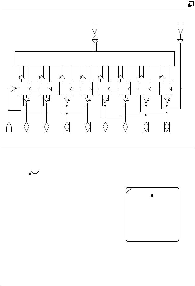
The PALCE16V8 is a universal PAL device. It has eight |
development software to verify the design and create a |
||
programming file (JEDEC). This file, once downloaded |
|||
independently configurable macrocells (MC0– MC7). |
|||
to a programmer, configures the device according to the |
|||
Each macrocell can be configured as registered output, |
|||
user's desired function. |
|||
combinatorial output, combinatorial I/O or dedicated in- |
|||
|
|
||
put. The programming matrix implements a program- |
The user is given two design options with the |
||
mable AND logic array, which drives a fixed OR logic |
PALCE16V8. First, it can be programmed as a standard |
||
array. Buffers for device inputs have complementary |
PAL device from the PAL16R8 and PAL10H8 series. |
||
outputs to provide user-programmable input signal po- |
The PAL programmer manufacturer will supply device |
||
larity. Pins 1 and 11 serve either as array inputs or as |
codes for the standard PAL device architectures to be |
||
clock (CLK) and output enable (OE), respectively, for all |
used with the PALCE16V8. The programmer will pro- |
||
flip-flops. |
gram the PALCE16V8 in the corresponding architec- |
||
Unused input pins should be tied directly to VCC or GND. |
ture. This allows the user to use existing standard PAL |
||
device JEDEC files without making any changes to |
|||
Product terms with all bits unprogrammed (discon- |
|||
them. Alternatively, the device can be programmed as |
|||
nected) assume the logical HIGH state and product |
|||
a PALCE16V8. Here the user must use the PALCE16V8 |
|||
terms with both true and complement of any input signal |
|||
device code. This option allows full utilization of the |
|||
connected assume a logical LOW state. |
|||
macrocell. |
|||
|
|||
The programmable functions on the PALCE16V8 are automatically configured from the user's design
|
|
|
|
To |
|
|
|
|
Adjacent |
|
|
|
1 1 |
Macrocell |
|
|
OE |
|
|
1 1 |
|
1 0 |
|
|
0 X |
|
VCC |
0 0 |
|
|
0 1 |
|
||
|
|
|
||
1 0 |
|
|
|
|
SL0 X |
|
|
|
|
SG1 |
|
|
1 1 |
|
|
|
|
|
|
|
|
|
0 X |
I/OX |
|
D |
Q |
1 0 |
|
|
|
|||
SL1X |
CLK |
Q |
|
|
|
|
|
1 0 |
|
|
|
|
1 1 |
From |
|
|
|
0 X |
|
|
|
|
Adjacent |
|
|
|
|
|
|
|
|
*SG1 |
SL0X |
Pin |
*In macrocells MC0 and MC7, SG1 is replaced by SG0 on the feedback multiplexer. |
|
16493D-4 |
||
|
|
|||
PALCE16V8 Macrocell
PALCE16V8 Family |
2-39 |

 AMD
AMD
Configuration Options |
|
use the feedback path of MC7 and pin 11 will use the |
||||||||
Each macrocell can be configured as one of the follow- |
feedback path of MC0. |
|
|
|||||||
|
|
|
|
|
|
|
|
|||
ing: registered output, combinatorial output, combinato- |
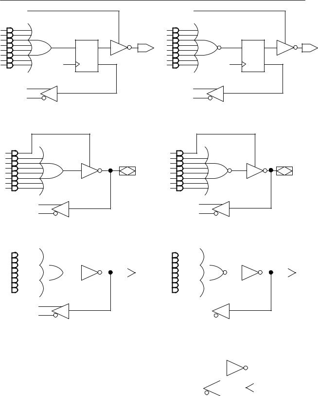
Combinatorial I/O in a Non-Registered |
|||||||||
rial I/O, or dedicated input. In |
the registered output |
|||||||||
Device |
|
|
|
|
|
|||||
configuration, the output buffer is enabled by the OE pin. |
|
|
|
|
|
|||||
|
|
|
|
|
|
|
|
|||
In the combinatorial configuration, the buffer is either |
The control bit settings are SG0 = 1, SG1 = 1, and SL0x = |
|||||||||
controlled by a product term or always enabled. In the |
1. Only seven product terms are available to the OR |
|||||||||
dedicated input configuration, it is always disabled. With |
gate. The eighth product term is used to enable the out- |
|||||||||
the exception of MC0 and MC7, a macrocell configured |
put buffer. The signal at the I/O pin is fed back to the |
|||||||||
as a dedicated input derives the input signal from an ad- |
AND array via the feedback multiplexer. This allows the |
|||||||||
jacent I/O. MC0 derives its input from pin 11 (OE) and |
pin to be used as an input. |
|
|
|||||||
MC7 from pin 1 (CLK). |
|
Because CLK and OE are not used in a non-registered |
||||||||
|
|
|||||||||
The macrocell configurations are controlled by the con- |
device, pins 1 and 11 are available as inputs. Pin 1 will |
|||||||||
figuration control word. It contains 2 global bits (SG0 |
use the feedback path of MC7 and pin 11 will use the |
|||||||||
and SG1) and 16 local bits (SL00 through SL07 and SL10 |
feedback path of MC0. |
|
|
|||||||
through SL17). SG0 determines whether registers will |
Combinatorial I/O in a Registered Device |
|||||||||
be allowed. SG1 determines whether the PALCE16V8 |
||||||||||
The control bit settings are SG0 = 0, SG1 = 1 and SL0x = |
||||||||||
will emulate a PAL16R8 family or a PAL10H8 family de- |
||||||||||
vice. Within each macrocell, SL0x, in conjunction with |
1. Only seven product terms are available to the OR |
|||||||||
SG1, selects the configuration of the macrocell, and |
gate. The eighth product term is used as the output |
|||||||||
SL1x sets the output as either active low or active high |
enable. The feedback signal is the corresponding I/O |
|||||||||
for the individual macrocell. |
|
signal. |
|
|
|
|
|
|
||
The configuration bits work by acting as control inputs |
Dedicated Input Configuration |
|||||||||
for the multiplexers in the macrocell. There are four mul- |
The control bit settings are SG0 = 1, SG1 = 0 and SL0x = |
|||||||||
tiplexers: a product term input, an enable select, an out- |
||||||||||
1. The output buffer is disabled. Except for MC0 and MC7 |
||||||||||
put select, and a feedback select multiplexer. SG1 and |
||||||||||
the feedback signal is an adjacent I/O. For MC0 and MC7 |
||||||||||
SL0x are the control signals for all four multiplexers. In |
||||||||||
the feedback signals are pins 1 and 11. These configu- |
||||||||||
MC0 and MC7, SG0 replaces SG1 on the feedback mul- |
||||||||||
rations are summarized in Table 1 and illustrated in |
||||||||||
tiplexer. This accommodates CLK being the adjacent |
||||||||||
Figure 2. |
|
|
|
|||||||
pin for MC7 and OE the adjacent pin for MC0. |
|
|
|
|||||||
|
|
|
Table 1. Macrocell Configuration |
|||||||
Registered Output Configuration |
|
|
|
|||||||
SG0 |
SG1 |
SL0X |
Cell Configuration |
Devices Emulated |
|
|||||
|
|
|
||||||||
The control bit settings are SG0 = 0, SG1 = 1 and SL0x = |
|
|
|
|
|
Device Uses Registers |
|
|||
0. There is only one registered configuration. All eight |
0 |
|
1 |
|
0 |
Registered Output |
PAL16R8, 16R6, |
|
||
product terms are available as inputs to the OR gate. |
0 |
|
1 |
|
1 |
Combinatorial I/O |
16R4 |
|
||
Data polarity is determined by |
SL1x. The flip-flop is |
|
|
PAL16R6, 16R4 |
|
|||||
|
|
|
|
Device Uses No Registers |
|
|||||
loaded on the LOW-to-HIGH transition of CLK. The |
|
|
|
|
|
|||||
1 |
|
0 |
|
0 |
Combinatorial |
PAL10H8, 12H6, |
|
|||
feedback path is from Q on the register. The output |
|
|
|
|||||||
|
|
|
|
|
Output |
14H4, 16H2, 10L8, |
|
|||
buffer is enabled by OE. |
|
|
|
|
|
|
|
|||
|
|
|
|
|
|
|
12L6, 14L4, 16L2 |
|
||
|
|
1 |
|
0 |
|
1 |
Input |
PAL12H6, 14H4, |
|
|
Combinatorial Configurations |
|
|
|
|
|
|
16H2, 12L6, 14L4, |
|
||
|
|
|
|
|
|
|
|
16L2 |
|
|
The PALCE16V8 has three combinatorial output con- |
1 |
|
1 |
|
1 |
Combinatorial I/O |
PAL16L8 |
|
||
figurations: dedicated output in a non-registered device, |
Programmable Output Polarity |
|||||||||
I/O in a non-registered device and I/O in a registered |
The polarity of each macrocell can be active-high or ac- |
|||||||||
device. |
|
|||||||||
|
tive-low, either to match output signal needs or to |
|||||||||
Dedicated Output in a Non-Registered |
||||||||||
reduce product terms. Programmable polarity allows |
||||||||||
Device |
|
Boolean expressions to be written in their most compact |
||||||||
The control bit settings are SG0 = 1, SG1 = 0 and SL0x = |
form (true or inverted), and the output can still be of the |
|||||||||
desired |
polarity. It can also save “DeMorganizing” |
|||||||||
0. All eight product terms are available to the OR gate. |
||||||||||
efforts. |
|
|
|
|
|
|
||||
Although the macrocell is a dedicated output, the feed- |
|
|
|
|
|
|
||||
|
|
|
|
|
|
|
|
|||
back is used, with the exception of pins 15 and 16. Pins |
Selection is through a programmable bit SL1x which |
|||||||||
15 and 16 do not use feedback in this mode. Because |
controls an exclusive-OR gate at the output of the AND/ |
|||||||||
CLK and OE are not used in a non-registered device, |
OR logic. The output is active high if SL1x is 1 and active |
|||||||||
pins 1 and 11 are available as input signals. Pin 1 will |
low if SL1x is 0. |
|
|
|
||||||
|
|
|
|
|
|
|
|
|
||
2-40 |
PALCE16V8 Family |
|
|
|
|
|
||||
AMD 
OE
D Q
CLK |
Q |
Registered Active Low
OE
D |
Q |
CLK |
Q |
Registered Active High
Combinatorial I/O Active Low |
|
|
Combinatorial I/O Active High |
|
|||||||||||
|
|
|
VCC |
|
|
|
|
|
|
VCC |
|
||||
|
|
|
|
|
|
|
|
|
|
|
|
|
|
|
|
|
|
|
|
|
|
|
|
|
|
|
|
|
|
|
|
|
|
|
|
|
|
|
|
|
|
|
|
|
|
|
|
|
|
|
|
|
|
|
|
|
|
|
|
|
|
|
|
|
|
|
|
|
|
|
|
|
|
|
|
|
|
|
|
|
|
|
|
|
|
|
|
|
|
|
|
|
|
|
|
|
|
|
|
|
|
|
|
|
|
|
|
|
|
|
|
Note 1 |
|
|
Note 1 |
|
|
|
|
|
|
|
|
Combinatorial Output Active Low |
Combinatorial Output Active High |
||||||||||
|
|
|
|
|
|
|
|
|
|
|
|
|
|
|
|
|
|
|
|
|
|
|
|
|
|
|
|
|
|
|
|
|
|
|
|
|
|
|
|
|
|
|
|
|
|
|
|
|
|
|
|
|
|
|
|
|
|
|
|
|
|
|
|
|
|
|
|
|
|
|
|
Notes: |
|
|
|
|
|
||||
1. |
Feedback is not available on pins 15 |
|
|
|
|
|
|
Adjacent I/O pin |
|
|
|
|
|
||||||
|
|
|
|
|
|||||
|
and 16 in the combinatorial output mode. |
|
|
|
|
|
|
||
|
|
|
|||||||
|
|
|
|
|
Note 2 |
||||
2. |
This configuration is not available on pins 15 and 16. |
|
|
|
|
||||
|
|||||||||
|
Dedicated Input |
|
16493D-5 |
Figure 2. Macrocell Configurations |
|
|
|
PALCE16V8 Family |
2-41 |

 AMD
AMD
Power-Up Reset
All flip-flops power up to a logic LOW for predictable system initialization. Outputs of the PALCE16V8 will depend on whether they are selected as registered or combinatorial. If registered is selected, the output will be HIGH. If combinatorial is selected, the output will be a function of the logic.
Register Preload
The register on the PALCE16V8 can be preloaded from the output pins to facilitate functional testing of complex state machine designs. This feature allows direct loading of arbitrary states, making it unnecessary to cycle through long test vector sequences to reach a desired state. In addition, transitions from illegal states can be verified by loading illegal states and observing proper recovery.
Security Bit
A security bit is provided on the PALCE16V8 as a deterrent to unauthorized copying of the array configuration patterns. Once programmed, this bit defeats readback and verification of the programmed pattern by a device programmer, securing proprietary designs from competitors. The bit can only be erased in conjunction with the array during an erase cycle.
Electronic Signature Word
An electronic signature word is provided in the PALCE16V8 device. It consists of 64 bits of programmable memory that can contain user-defined data. The signature data is always available to the user independent of the security bit.
Programming and Erasing
The PALCE16V8 can be programmed on standard logic programmers. It also may be erased to reset a previously configured device back to its virgin state. Erasure is automatically performed by the programming hardware. No special erase operation is required.
Quality and Testability
The PALCE16V8 offers a very high level of built-in quality. The erasability of the device provides a direct means of verifying performance of all AC and DC parameters. In addition, this verifies complete programmability and functionality of the device to provide the highest programming yields and post-programming functional yields in the industry.
Technology
The high-speed PALCE16V8 is fabricated with AMD's advanced electrically erasable (EE) CMOS process. The array connections are formed with proven EE cells. Inputs and outputs are designed to be compatible with TTL devices. This technology provides strong input clamp diodes, output slew-rate control, and a grounded substrate for clean switching.
PCI Compliance
The PALCE22V10H-7/10 is fully compliant with the PCI Local Bus Specification published by the PCI Special Interest Group. The PALCE22V10H-7/10's predictable timing ensures compliance with the PCI AC specifications independent of the design.
2-42 |
PALCE16V8 Family |

|
|
|
|
|
|
|
|
|
|
|
|
|
|
|
|
|
AMD |
|
LOGIC DIAGRAM |
|
|
|
|
|
|
|
|
|
|
|
|
|
|
|
|||
|
0 |
3 |
4 |
7 |
8 |
11 12 |
15 |
16 |
19 |
20 |
23 24 |
27 28 |
31 |
|
|
|
|
|
CLK/I0 |
1 |
|
|
|
|
|
|
|
|
|
|
|
|
|
|
|
|
|
|
|
|
|
|
|
|
|
|
|
|
|
|
1 1 |
|
|
1 1 |
20 VCC |
|
|
|
|
|
|
|
|
|
|
|
|
|
|
|
|
1 0 |
|
|
|
|
|
|
|
|
|
|
|
|
|
|
|
|
0 X |
|
VCC |
0 0 |
|
|
|
|
|
|
|
|
|
|
|
|
|
|
|
|
|
0 1 |
|
|
|
|
|
|
|
|
|
|
|
|
|
|
|
|
1 0 |
|
|
|
|
|
|
0 |
|
|
|
|
|
|
|
|
|
|
|
|
SL07 |
|
|
|
|
|
|
|
|
|
|
|
|
|
|
|
|
|
SG1 |
|
|
|
|
|
|
|
|
|
|
|
|
|
|
|
|
|
|
|
|
1 1 |
|
|
|
|
|
|
|
|
|
|
|
|
|
|
|
|
|
|
|
|
|
|
|
|
|
|
|
|
|
|
|
|
|
|
|
|
|
|
0 X |
19 |
I/O7 |
|
|
|
|
|
|
|
|
|
|
|
|
|
|
D |
Q |
1 0 |
||
|
|
|
|
|
|
|
|
|
|
|
|
|
|
|
|
|||
|
7 |
|
|
|
|
|
|
|
|
|
|
|
|
SL17 |
Q |
|
|
|
|
|
|
|
|
|
|
|
|
|
|
|
|
|
|
|
|
|
|
|
|
|
|
|
|
|
|
|
|
|
|
|
|
|
|
1 0 |
|
|
I1 |
2 |
|
|
|
|
|
|
|
|
|
|
|
|
|
|
1 1 |
|
|
|
|
|
|
|
|
|
|
|
|
|
|
|
|
0 X |
|
|
||
|
|
|
|
|
|
|
|
|
|
|
|
|
|
|
SG0 |
|
SL0 7 |
|
|
|
|
|
|
|
|
|
|
|
|
|
|
|
|
|
1 1 |
|
|
|
|
|
|
|
|
|
|
|
|
|
|
|
1 1 |
|
|
1 0 |
|
|
|
|
|
|
|
|
|
|
|
|
|
|
|
0 X |
|
VCC |
0 0 |
|
|
|
|
|
|
|
|
|
|
|
|
|
|
|
|
|
0 1 |
|
|
|
|
|
|
|
|
|
|
|
|
|
|
|
|
1 0 |
|
|
|
|
|
|
8 |
|
|
|
|
|
|
|
|
|
|
|
|
SL06 |
|
|
|
|
|
|
|
|
|
|
|
|
|
|
|
|
|
SG1 |
|
1 1 |
|
|
|
|
|
|
|
|
|
|
|
|
|
|
|
|
|
|
|
|
||
|
|
|
|
|
|
|
|
|
|
|
|
|
|
|
|
|
|
|
|
|
|
|
|
|
|
|
|
|
|
|
|
|
|
|
0 X |
18 |
I/O6 |
|
|
|
|
|
|
|
|
|
|
|
|
|
|
D |
Q |
1 0 |
||
|
15 |
|
|
|
|
|
|
|
|
|
|
|
|
SL16 |
Q |
|
|
|
|
|
|
|
|
|
|
|
|
|
|
|
|
|
|
|
|
|
|
|
|
|
|
|
|
|
|
|
|
|
|
|
|
|
|
1 0 |
|
|
I2 |
3 |
|
|
|
|
|
|
|
|
|
|
|
|
|
|
1 1 |
|
|
|
|
|
|
|
|
|
|
|
|
|
|
|
|
0 X |
|
|
||
|
|
|
|
|
|
|
|
|
|
|
|
|
|
|
SG1 |
|
SL0 6 |
|
|
|
|
|
|
|
|
|
|
|
|
|
|
|
|
|
1 1 |
|
|
|
|
|
|
|
|
|
|
|
|
|
|
|
1 1 |
|
|
1 0 |
|
|
|
|
|
|
|
|
|
|
|
|
|
|
|
0 X |
|
VCC |
0 0 |
|
|
|
|
|
|
|
|
|
|
|
|
|
|
|
|
|
0 1 |
|
|
|
|
|
|
|
|
|
|
|
|
|
|
|
|
1 0 |
|
|
|
|
|
|
16 |
|
|
|
|
|
|
|
|
|
|
|
|
SL05 |
|
|
|
|
|
|
|
|
|
|
|
|
|
|
|
|
|
SG1 |
|
|
|
|
|
|
|
|
|
|
|
|
|
|
|
|
|
|
|
|
1 1 |
|
|
|
|
|
|
|
|
|
|
|
|
|
|
|
|
|
|
|
|
|
|
|
|
|
|
|
|
|
|
|
|
|
|
|
|
|
|
0 X |
17 I/O5 |
|
|
|
|
|
|
|
|
|
|
|
|
|
|
|
D |
Q |
1 0 |
||
|
23 |
|
|
|
|
|
|
|
|
|
|
|
|
SL15 |
Q |
|
|
|
|
|
|
|
|
|
|
|
|
|
|
|
|
|
|
|
|
|
|
|
|
|
|
|
|
|
|
|
|
|
|
|
|
|
|
1 0 |
|
|
I3 |
4 |
|
|
|
|
|
|
|
|
|
|
|
|
|
|
1 1 |
|
|
|
|
|
|
|
|
|
|
|
|
|
|
|
|
0 X |
|
|
||
|
|
|
|
|
|
|
|
|
|
|
|
|
|
|
SG1 |
|
SL0 5 |
|
|
|
|
|
|
|
|
|
|
|
|
|
|
|
|
|
1 1 |
|
|
|
|
|
|
|
|
|
|
|
|
|
|
|
1 1 |
|
|
1 0 |
|
|
|
|
|
|
|
|
|
|
|
|
|
|
|
0 X |
|
VCC |
0 0 |
|
|
|
|
|
|
|
|
|
|
|
|
|
|
|
|
|
0 1 |
|
|
|
|
|
|
|
|
|
|
|
|
|
|
|
|
1 0 |
|
|
|
|
|
|
24 |
|
|
|
|
|
|
|
|
|
|
|
|
SL04 |
|
|
|
|
|
|
|
|
|
|
|
|
|
|
|
|
|
SG1 |
|
1 1 |
|
|
|
|
|
|
|
|
|
|
|
|
|
|
|
|
|
|
|
|
|
|
|
|
|
|
|
|
|
|
|
|
|
|
|
|
|
|
0 X |
16 I/O4 |
|
|
|
|
|
|
|
|
|
|
|
|
|
|
|
D |
Q |
1 0 |
||
|
|
|
|
|
|
|
|
|
|
|
|
|
|
|
|
|||
|
31 |
|
|
|
|
|
|
|
|
|
|
|
|
SL14 |
Q |
|
|
|
|
|
|
|
|
|
|
|
|
|
|
|
|
|
|
|
|
|
|
|
|
|
|
|
|
|
|
|
|
|
|
|
|
|
|
1 0 |
|
|
I4 |
5 |
|
|
|
|
|
|
|
|
|
|
|
|
|
|
1 1 |
|
|
|
|
|
|
|
|
|
|
|
|
|
|
|
|
0 X |
|
|
||
|
|
|
|
|
|
|
|
|
|
|
|
|
|
|
SG1 |
|
SL0 4 |
|
|
0 |
3 |
4 |
7 |
8 |
11 12 |
15 16 |
19 20 |
23 24 |
27 28 |
31 |
CLK OE |
|
|
|
|
||
|
|
|
|
|
|
|
|
|
|
|
|
|
|
|
|
|
16493D-6 |
|
|
|
|
|
|
|
|
|
|
|
|
PALCE16V8 Family |
|
|
|
|
2-43 |
||
 Loading...