


AMD MACH211SP-12JI, MACH211SP-12JC, MACH211SP-10VC, MACH211SP-10JI, MACH211SP-10JC Datasheet
...FINAL |
COM’L: -7.5/10/12/15/20 |
IND: -10/12/14/18/24 |
|
|
|
MACH211SP-7/10/12/15/20
High-Density EE CMOS Programmable Logic
DISTINCTIVE CHARACTERISTICS
■ JTAG-Compatible, 5-V in-system programming |
■ Peripheral Component Interconnect (PCI) |
|
■ 44 |
Pins |
compliant (-7/-10) |
|
||
■ 64 |
Macrocells |
■ Programmable power-down mode |
|
||
■ 7.5 ns tPD Commercial |
■ 32 Outputs |
|
|
||
10 ns tPD Industrial |
■ 64 Flip-flops; 2 clock choices |
|
■ 133 MHz fCNT |
■ 4 “PAL26V16” blocks with buried macrocells |
|
■ 34 |
Bus-Friendly™ Inputs and I/Os |
■ Improved routing over the MACH210 |
IN-SYSTEM PROGRAMMING
In-system programming allows the MACH211SP to be programmed while soldered onto a system board. Programming the MACH211SP in-system yields numerous benefits at all stages of development: prototyping, manufacturing, and in the field. Since insertion into a programmer isn’t needed, multiple handling steps and the resulting bent leads are eliminated. The design can be modified in-system for design changes and debugging while prototyping, programming boards in production, and field upgrades.
The MACH211SP offers advantages not available in other CPLD architectures with in-system programming. MACH devices have extensive routing resources for pin-out retention; design changes resulting in pin-out changes for other CPLDs cancel the advantages of in-system programming. The MACH211SP can be employed in any JTAG (IEEE 1149.1) compliant chain.
GENERAL DESCRIPTION
The MACH211SP is a member of AMD’s EE CMOS Performance Plus MACH 2 device family. This device has approximately six times the logic macrocell capability of the popular PAL22V10 without loss of speed.
The MACH211SP consists of four PAL blocks interconnected by a programmable switch matrix. The four PAL blocks are essentially “PAL26V16” structures complete with product-term arrays and programmable macrocells, which can be programmed as high speed or low power, and buried macrocells. The switch matrix connects the PAL blocks to each other and to all input pins, providing a high degree of connectivity between the fully-connected PAL blocks. This allows designs to be placed and routed efficiently.
The MACH211SP has two kinds of macrocell: output and buried. The MACH211SP output macrocell provides registered, latched, or combinatorial outputs with
programmable polarity. If a registered configuration is chosen, the register can be configured as D-type or T-type to help reduce the number of product terms. The register type decision can be made by the designer or by the software. All output macrocells can be connected to an I/O cell. If a buried macrocell is desired, the internal feedback path from the macrocell can be used, which frees up the I/O pin for use as an input.
The MACH211SP has dedicated buried macrocells which, in addition to the capabilities of the output macrocell, also provide input registers or latches for use in synchronizing signals and reducing setup time requirements.
The MACH211SP is an enhanced version of the MACH211, adding the JTAG-compatible in-system programming feature.
Publication# 20405 Rev: B Amendment/0
Issue Date: February 1996

BLOCK DIAGRAM
I/O0–I/O7 |
I/O8–I/O15 |
||
|
8 |
|
8 |
I/O Cells |
8 |
I/O Cells |
8 |
|
|
||
8 |
8 |
8 |
8 |
Macrocells |
Macrocells |
Macrocells |
2 |
Macrocells |
|||
|
OE |
|
OE |
|
52 x 68 |
|
52 x 68 |
AND Logic Array |
AND Logic Array |
||
|
and |
|
and |
|
Logic Allocator |
|
Logic Allocator |
|
26 |
|
26 |
|
|
Switch Matrix |
|
|
|
26 |
|
|
52 x 68 |
AND Logic Array |
||
|
|
and |
|
Logic Allocator |
|
|
|
OE |
Macrocells |
|
Macrocells |
8 |
8 |
8 |
|
||
|
|
|
I/O Cells |
|
|
|
8 |
|
I/O24–I/O31 |
|
|
|
26 |
|
|
52 x 68 |
|
AND Logic Array |
|
|
|
and |
2 |
|
Logic Allocator |
|
|
OE |
|
Macrocells |
Macrocells |
2 |
|
||
8 |
8 |
|
8 |
|
|
|
|
|
I/O Cells |
|
|
|
8 |
|
I/O16–I/O23 |
CLK0/I0 |
|
|
|
|
|
|
CLK1/I1 |
20405B-1
2 |
MACH211SP-7/10/12/15/20 |
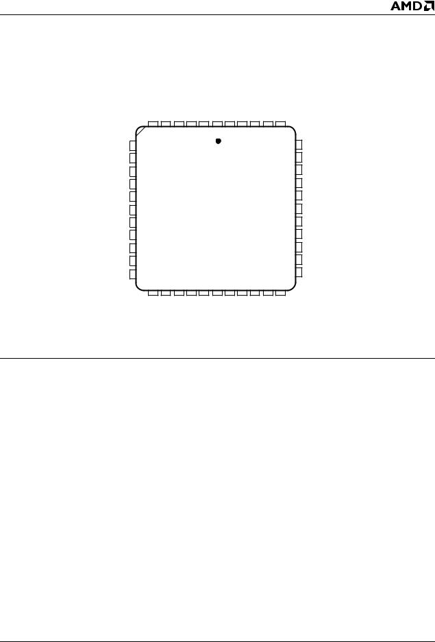
CONNECTION DIAGRAM MACH211SP
Top View
44-Pin PLCC
|
|
|
I/O4 |
I/O3 |
I/O2 |
I/O1 |
I/O0 |
GND |
VCC |
I/O31 |
I/O30 |
I/O29 |
I/O28 |
|
|
|
|
5 |
4 |
3 |
2 |
1 |
44 |
43 42 |
41 40 |
|
|||
|
|
|
6 |
|
||||||||||
I/O5 |
7 |
|
|
|
|
|
|
|
|
|
|
39 |
I/O27 |
|
I/O6 |
8 |
|
|
|
|
|
|
|
|
|
|
38 |
I/O26 |
|
I/O7 |
9 |
|
|
|
|
|
|
|
|
|
|
37 |
I/O25 |
|
TDI |
10 |
|
|
|
|
|
|
|
|
|
36 |
I/O24 |
||
CLK0/I0 |
11 |
|
|
|
|
|
|
|
|
|
35 |
TDO |
||
GND |
12 |
|
|
|
|
|
|
|
|
|
34 |
GND |
||
TCK |
13 |
|
|
|
|
|
|
|
|
|
33 |
CLK1/I1 |
||
I/O8 |
14 |
|
|
|
|
|
|
|
|
|
32 |
TMS |
||
I/O9 |
15 |
|
|
|
|
|
|
|
|
|
31 |
I/O23 |
||
I/O10 |
16 |
|
|
|
|
|
|
|
|
|
30 |
I/O22 |
||
I/O11 |
17 |
|
|
|
|
|
|
|
|
|
29 |
I/O21 |
||
|
18 |
19 20 |
21 22 |
23 24 |
25 26 |
27 28 |
|
|||||||
|
|
|
I/O12 |
I/O13 |
I/O14 |
I/O15 |
VCC |
GND |
I/O16 |
I/O17 |
I/O18 |
I/O19 |
I/O20 |
|
20405B-2
PIN DESIGNATIONS
CLK/I = |
Clock or Input |
TDI |
= |
Test Data In |
|
GND |
= Ground |
TCK |
= Test Clock |
||
I |
= |
Input |
TMS |
= |
Test Mode Select |
I/O |
= |
Input/Output |
TDO |
= |
Test Data Out |
VCC |
= |
Supply Voltage |
|
|
|
MACH211SP-7/10/12/15/20 |
3 |
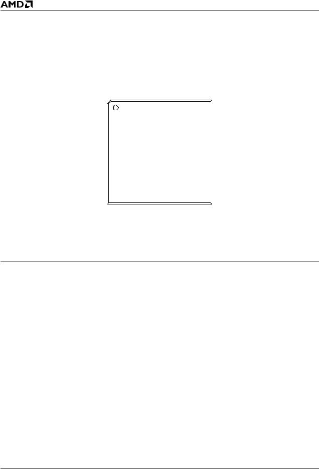
CONNECTION DIAGRAM MACH211SP
Top View
44-Pin TQFP
|
|
|
I/O4 |
I/O3 |
I/O2 |
I/O1 |
I/O0 |
GND |
VCC |
I/O31 |
I/O30 |
I/O29 |
I/O28 |
|
|
|||||||||||||||||
|
|
|
|
|
|
|
|
|
|
|
|
|
|
|
|
|
|
|
|
|
|
|
|
|
|
|
|
|
|
|
|
|
|
|
|
|
|
|
|
|
|
|
|
|
|
|
|
|
|
|
|
|
|
|
|
|
|
|
|
|
|
|
|
|
|
|
|
|
|
|
|
|
|
|
|
|
|
|
|
|
|
|
|
|
|
|
|
|
|
|
|
|
|
|
|
|
|
|
|
|
|
44 |
43 |
42 |
41 |
40 |
39 |
38 |
37 |
|
36 |
|
35 |
|
34 |
|
|
|
|
||||||||||||
I/O5 |
|
|
1 |
|
|
|
|
|
|
|
|
|
|
|
|
|
|
|
|
|
|
|
|
|
|
33 |
|
|
|
I/O27 |
||
|
|
|
|
|
|
|
|
|
|
|
|
|
|
|
|
|
|
|
|
|
|
|
|
|
|
|||||||
|
|
|
|
|
|
|
|
|
|
|
|
|
|
|
|
|
|
|
|
|
|
|
|
|
|
|||||||
I/O6 |
|
|
2 |
|
|
|
|
|
|
|
|
|
|
|
|
|
|
|
|
|
|
|
|
|
|
32 |
|
|
|
I/O26 |
||
|
|
|
|
|
|
|
|
|
|
|
|
|
|
|
|
|
|
|
|
|
|
|
|
|
|
|||||||
|
|
|
|
|
|
|
|
|
|
|
|
|
|
|
|
|
|
|
|
|
|
|
|
|
|
|||||||
I/O7 |
|
|
3 |
|
|
|
|
|
|
|
|
|
|
|
|
|
|
|
|
|
|
|
|
|
|
31 |
|
|
|
I/O25 |
||
|
|
|
|
|
|
|
|
|
|
|
|
|
|
|
|
|
|
|
|
|
|
|
|
|
|
|||||||
|
|
|
|
|
|
|
|
|
|
|
|
|
|
|
|
|
|
|
|
|
|
|
|
|
|
|||||||
TDI |
|
|
4 |
|
|
|
|
|
|
|
|
|
|
|
|
|
|
|
|
|
|
|
|
|
|
30 |
|
|
|
I/O24 |
||
|
|
|
|
|
|
|
|
|
|
|
|
|
|
|
|
|
|
|
|
|
|
|
|
|
|
|||||||
|
|
|
|
|
|
|
|
|
|
|
|
|
|
|
|
|
|
|
|
|
|
|
|
|
|
|||||||
CLK0/I0 |
|
|
5 |
|
|
|
|
|
|
|
|
|
|
|
|
|
|
|
|
|
|
|
|
|
|
29 |
|
|
|
TDO |
||
|
|
|
|
|
|
|
|
|
|
|
|
|
|
|
|
|
|
|
|
|
|
|
|
|
|
|||||||
|
|
|
|
|
|
|
|
|
|
|
|
|
|
|
|
|
|
|
|
|
|
|
|
|
|
|||||||
GND |
|
|
6 |
|
|
|
|
|
|
|
|
|
|
|
|
|
|
|
|
|
|
|
|
|
|
28 |
|
|
|
GND |
||
|
|
|
|
|
|
|
|
|
|
|
|
|
|
|
|
|
|
|
|
|
|
|
|
|
|
|||||||
|
|
|
|
|
|
|
|
|
|
|
|
|
|
|
|
|
|
|
|
|
|
|
|
|
|
|||||||
TCK |
|
|
7 |
|
|
|
|
|
|
|
|
|
|
|
|
|
|
|
|
|
|
|
|
|
|
27 |
|
|
|
CLK1/I1 |
||
|
|
|
|
|
|
|
|
|
|
|
|
|
|
|
|
|
|
|
|
|
|
|
|
|
|
|||||||
|
|
|
|
|
|
|
|
|
|
|
|
|
|
|
|
|
|
|
|
|
|
|
|
|
|
|||||||
I/O8 |
|
|
8 |
|
|
|
|
|
|
|
|
|
|
|
|
|
|
|
|
|
|
|
|
|
|
26 |
|
|
|
TMS |
||
|
|
|
|
|
|
|
|
|
|
|
|
|
|
|
|
|
|
|
|
|
|
|
|
|
|
|||||||
|
|
|
|
|
|
|
|
|
|
|
|
|
|
|
|
|
|
|
|
|
|
|
|
|
|
|||||||
I/O9 |
|
|
9 |
|
|
|
|
|
|
|
|
|
|
|
|
|
|
|
|
|
|
|
|
|
|
25 |
|
|
|
I/O23 |
||
|
|
|
|
|
|
|
|
|
|
|
|
|
|
|
|
|
|
|
|
|
|
|
|
|
|
|||||||
|
|
|
|
|
|
|
|
|
|
|
|
|
|
|
|
|
|
|
|
|
|
|
|
|
|
|||||||
I/O10 |
|
|
10 |
|
|
|
|
|
|
|
|
|
|
|
|
|
|
|
|
|
|
|
|
|
|
24 |
|
|
|
I/O22 |
||
|
|
|
|
|
|
|
|
|
|
|
|
|
|
|
|
|
|
|
|
|
|
|
|
|
|
|||||||
|
|
|
|
|
|
|
|
|
|
|
|
|
|
|
|
|
|
|
|
|
|
|
|
|
|
|||||||
I/O11 |
|
|
11 |
|
|
|
|
|
|
|
|
|
|
|
|
|
|
|
|
|
|
|
|
|
|
23 |
|
|
|
I/O21 |
||
|
|
|
|
|
|
|
|
|
|
|
|
|
|
|
|
|
|
|
|
|
|
|
|
|
|
|||||||
|
|
|
|
|
|
|
|
|
|
|
|
|
|
|
|
|
|
|
|
|
|
|
|
|
|
|||||||
|
|
|
12 |
13 |
14 |
15 |
16 |
17 |
18 |
19 |
|
20 |
|
21 |
|
22 |
|
|
|
|
|
|||||||||||
|
|
|
|
|
|
|
|
|
|
|
|
|
|
|
|
|
|
|
|
|
|
|
|
|
|
|
|
|
|
|
|
|
|
|
|
|
|
|
|
|
|
|
|
|
|
|
|
|
|
|
|
|
|
|
|
|
|
|
|
|
|
|
|
|
|
|
|
|
I/O12 |
I/O13 |
I/O14 |
I/O15 |
VCC |
GND |
I/O16 |
I/O17 |
I/O18 |
I/O19 |
I/O20 |
|
|
|||||||||||||||||
20405B-3
PIN DESIGNATIONS
CLK/I = |
Clock or Input |
TDI |
= |
Test Data In |
|
GND |
= Ground |
TCK |
= Test Clock |
||
I |
= |
Input |
TMS |
= |
Test Mode Select |
I/O |
= |
Input/Output |
TDO |
= |
Test Data Out |
VCC |
= Supply Voltage |
|
|
|
|
4 |
MACH211SP-7/10/12/15/20 |
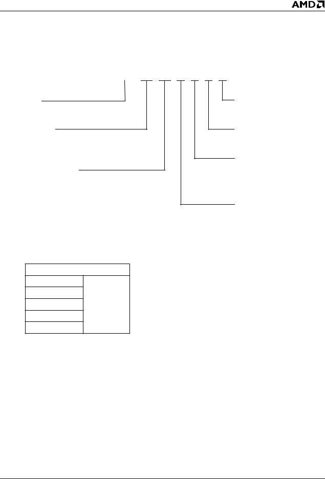
ORDERING INFORMATION
Commercial Products
AMD programmable logic products for commercial applications are available with several ordering options. The order number (Valid Combination) is formed by a combination of:
MACH 211 SP -7 J C
FAMILY TYPE
MACH = Macro Array CMOS High-Speed
DEVICE NUMBER
211 = 64 Macrocells, 44 Pins,
Power-Down mode,
Bus-Friendly Inputs and I/Os
PRODUCT DESIGNATION
SP = In-system Programmable
OPTIONAL PROCESSING
Blank = Standard Processing
OPERATING CONDITIONS
C = Commercial (0°C to +70°C)
PACKAGE TYPE
J= 44-Pin Plastic Leaded Chip Carrier (PL 044)
V = 44-Pin Thin Quad Flat Pack
(PQT044)
SPEED
-7 = 7.5 ns tPD -10 = 10 ns tPD -12 = 12 ns tPD -15 = 15 ns tPD -20 = 20 ns tPD
Valid Combinations
MACH211SP-7
MACH211SP-10
MACH211SP-12 |
JC, VC |
MACH211SP-15
MACH211SP-20
Valid Combinations
The Valid Combinations table lists configurations planned to be supported in volume for this device. Consult the local AMD sales office to confirm availability of specific valid combinations and to check on newly released combinations.
MACH211SP-7/10/12/15/20 (Com’l) |
5 |
ORDERING INFORMATION
Industrial Products
AMD programmable logic products for industrial applications are available with several ordering options. The order number (Valid Combination) is formed by a combination of:
|
|
MACH 211 SP -10 J |
|
I |
|||||||||||||||||||
FAMILY TYPE |
|
|
|
|
|
|
|
|
|
|
|
|
|
|
|
|
|
|
|
|
OPTIONAL PROCESSING |
||
|
|
|
|
|
|
|
|
|
|
|
|
|
|
|
|
|
|||||||
MACH = Macro Array CMOS High-Speed |
|
|
|
|
|
|
|
|
|
|
|
|
|
|
|
|
|
|
|
Blank = Standard Processing |
|||
DEVICE NUMBER |
|
|
|
|
|
|
|
|
|
|
|
|
|
|
|
|
|
|
|
|
|
OPERATING CONDITIONS |
|
|
|
|
|
|
|
|
|
|
|
|
|
|
|
|
|
|
|
||||||
211 = 64 Macrocells, 44 Pins, |
|
|
|
|
|
|
|
|
|
|
|
|
|
|
|
|
I = Industrial (–40°C to +85°C) |
||||||
Power-Down mode, |
|
|
|
|
|
|
|
|
|
|
|
|
|
|
|
|
|
||||||
Bus-Friendly Inputs and I/Os |
|
|
|
|
|
|
|
|
|
|
|
|
|
|
|
|
|
||||||
|
|
|
|
|
|
|
|
|
|
|
|
|
|
|
|
|
|
|
|
|
|
|
PACKAGE TYPE |
|
|
|
|
|
|
|
|
|
|
|
|
|
|
|
|
|
|
|
|
|
|
|
|
PRODUCT DESIGNATION |
|
|
|
|
|
|
|
|
|
|
|
|
|
|
|
|
|
|
|
|
|
J = 44-Pin Plastic Leaded Chip |
|
|
|
|
|
|
|
|
|
|
|
|
|
|
|
|
|
|
|
|
|
|
Carrier (PL 044) |
||
SP = In-system Programmable |
|
|
|
|
|
|
|
|
|
|
|
|
|
||||||||||
|
|
|
|
|
|
|
|
|
|
|
|
|
|||||||||||
|
|
|
|
|
|
|
|
|
|
|
|
|
|
|
|
|
|
|
|
|
|
|
SPEED |
|
|
|
|
|
|
|
|
|
|
|
|
|
|
|
|
|
|
|
|
|
|
|
|
Valid Combinations
MACH211SP-10
MACH211SP-12
MACH211SP-14 JI
MACH211SP-18
MACH211SP-24
-10 = 10 ns tPD -12 = 12 ns tPD -14 = 14.5 ns tPD -18 = 18 ns tPD -24 = 24 ns tPD
Valid Combinations
The Valid Combinations table lists configurations planned to be supported in volume for this device. Consult the local AMD sales office to confirm availability of specific valid combinations and to check on newly released combinations.
6 |
MACH211SP-10/12/14/18/24 (Ind) |

FUNCTIONAL DESCRIPTION
The MACH211SP consists of four PAL blocks connected by a switch matrix.There are 32 I/O pins feeding the switch matrix. These signals are distributed to the four PAL blocks for efficient design implementation. There are two clock pins that can also be used as dedicated inputs.
The PAL Blocks
Each PAL block in the MACH211SP (Figure 1) contains a 64-product-term logic array, a logic allocator, 8 output macrocells, 8 buried macrocells, and 8 I/O cells. The switch matrix feeds each PAL block with 26 inputs. This makes the PAL block look effectively like an independent “PAL26V16” with 8 buried macrocells.
In addition to the logic product terms, two output enable product terms, an asynchronous reset product term, and an asynchronous preset product term are provided. One of the two output enable product terms can be chosen within each I/O cell in the PAL block. All flip-flops within the PAL block are initialized together.
The Switch Matrix
The MACH211SP switch matrix is fed by the inputs and feedback signals from the PAL blocks. Each PAL block provides 16 internal feedback signals and 8 I/O feedback signals. The switch matrix distributes these signals back to the PAL blocks in an efficient manner that also provides for high performance. The design software automatically configures the switch matrix when fitting a design into the device.
The Product-term Array
The MACH211SP product-term array consists of 64 product terms for logic use, and 4 special-purpose product terms. Two of the special-purpose product terms provide programmable output enable; one provides asynchronous reset, and one provides asynchronous preset.
The Logic Allocator
The logic allocator in the MACH211SP takes the 64 logic product terms and allocates them to the 16 macrocells as needed. Each macrocell can be driven by up to 16 product terms. The design software automatically configures the logic allocator when fitting the design into the device.
Table 1 illustrates which product term clusters are available to each macrocell within a PAL block. Refer to Figure 1 for cluster and macrocell numbers.
The Macrocell
The MACH211SP has two types of macrocell: output and buried. The output macrocells can be configured as either registered, latched, or combinatorial, with programmable polarity. The macrocell provides internal
|
Table 1. |
Logic Allocation |
|
|
|
|
|
Macrocell |
|
|
|
|
|
|
|
Output |
Buried |
|
Available Clusters |
|
|
|
|
M0 |
|
|
C0, C1, C2 |
|
M1 |
|
C0, C1, C2, C3 |
|
|
|
|
M2 |
|
|
C1, C2, C3, C4 |
|
M3 |
|
C2, C3, C4, C5 |
|
|
|
|
M4 |
|
|
C3, C4, C5, C6 |
|
M5 |
|
C4, C5, C6, C7 |
M6 |
|
|
C5, C6, C7, C8 |
|
M7 |
|
C6, C7, C8, C9 |
M8 |
|
|
C7, C8, C9, C10 |
|
M9 |
|
C8, C9, C10, C11 |
M10 |
|
|
C9, C10, C11, C12 |
|
M11 |
|
C10, C11, C12, C13 |
M12 |
|
|
C11, C12, C13, C14 |
|
M13 |
|
C12, C13, C14, C15 |
M14 |
|
|
C13, C14, C15 |
|
M15 |
|
C14, C15 |
feedback whether configured with or without the flip-flop. The registers can be configured as D-type or T-type, allowing for product-term optimization.
The flip-flops can individually select one of two clock/ gate pins, which are also available as data inputs. The registers are clocked on the LOW-to-HIGH transition of the clock signal. The latch holds its data when the gate input is HIGH, and is transparent when the gate input is LOW. The flip-flops can also be asynchronously initialized with the common asynchronous reset and preset product terms.
The buried macrocells are the same as the output macrocells if they are used for generating logic. In that case, the only thing that distinguishes them from the output macrocells is the fact that there is no I/O cell connection, and the signal is only used internally. The buried macrocell can also be configured as an input register or latch.
The I/O Cell
The I/O cell in the MACH211SP consists of a three-state output buffer. The three-state buffer can be configured in one of three ways: always enabled, always disabled, or controlled by a product term. If product term control is chosen, one of two product terms may be used to provide the control. The two product terms that are available are common to all I/O cells in a PAL block.
MACH211SP-7/10/12/15/20 |
7 |

These choices make it possible to use the macrocell as an output, an input, a bidirectional pin, or a three-state output for use in driving a bus.
Power-Down Mode
The MACH211SP features a programmable low-power mode in which individual signal paths can be programmed as low power. These low-power speed paths will be slightly slower than the non-low-power paths. This feature allows speed critical paths to run at maximum frequency while the rest of the paths operate in the low-power mode, resulting in power savings of up to 75%. If all signals in a PAL block are low-power, then total power is reduced further.
In-System Programming
Programming is the process where MACH devices are loaded with a pattern defined in a JEDEC file obtained from MACHXL software or third-party software. Programming is accomplished through four JTAG pins: Test Mode Select (TMS), Test Clock (TCK), Test Data In (TDI), and Test Data Out (TDO). The MACH211SP can be employed in any JTAG (IEEE 1149.1) compliant chain. While the MACH211SP is fully JTAG compatible, it supports the BYPASS instruction, not the EXTEST and SAMPLE/PRELOAD instructions. The MACH211SP can be programmed across the commercial temperature range. Programming the MACH device after it has been placed on a circuit board is easily accomplished. Programming is initiated by placing the device into programming mode, using the MACHPRO programming software provided by AMD. The device is bulk erased and the JEDEC file is then loaded. After the data is transferred into the device, the PROGRAM instruction is loaded. Further programming details can be found in application note, “Advanced In-circuit Programming Guidelines.”
should be programmed. The configuration file is discussed in detail in the MACHPRO software manual.
The MACH211SP devices tristate the outputs during programming. They have one security bit which inhibits program and verify. This allows the user to protect proprietary patterns and designs.
Program verification of a MACH device involves reading back the programmed pattern and comparing it with the original JEDEC file. The AMD method of program verification performed on the MACH devices permits the verification of one device at a time.
Accidental Programming or Erasure Protection
It is virtually impossible to program or erase a MACH device inadvertently. The following conditions must be met before programming actually takes place:
■The device must be in the password-protected program mode
■The programming or bulk erase instruction must be in the instruction register
If the above conditions are not met, the programming circuitry cannot be activated.
To ensure that the AMD ten year device data retention guarantee applies, 100 program/erase cycle limit should not be exceeded.
Bus-Friendly Inputs and I/Os
The MACH211SP inputs and I/Os include two inverters in series which loop back to the input. This double inversion reinforces the state of the input and pulls the voltage away from the input threshold voltage. For an illustration of this configuration, please turn to the Input/Output Equivalent Schematics section.
On-Board Programming Options |
PCI Compliance |
Since the MACHPRO software performs these steps automatically, the following programming options are published for reference.
The configuration file, which is also known as the chain file, defines the MACH device JTAG chain. The file contains the information concerning which JEDEC file is to be placed into which device, the state which the outputs should be placed, and whether the security fuses
The MACH211SP-7/10 is fully compliant with the PCI Local Bus Specificationpublished by the PCI Special Interest Group. The MACH211SP-7/10’s predictable timing ensures compliance with the PCI AC specifications independent of the design. On the other hand, in CPLD and FPGA architectures without predictable timing, PCI compliance is dependent upon routing and product term distribution.
8 |
MACH211SP-7/10/12/15/20 |

0 |
4 |
8 |
12 |
16 |
20 |
24 |
28 |
32 |
36 |
40 |
43 |
47 |
51 |
Output Enable
Output Enable
Asynchronous Reset
Asynchronous Preset
|
|
|
|
|
|
|
|
|
|
|
|
|
|
|
|
|
|
|
I/O |
I/O |
|
|
|
|
|
|
|
|
|
|
|
|
|
|
|
|
|
|
Output |
Cell |
|
|
|
|
|
|
|
|
|
|
|
|
|
|
|
|
|
|
|
|
|
|
|
|
|
|
|
|
|
|
|
|
|
|
|
|
|
|
M0 |
Macro |
|
|
|
|
|
|
|
|
|
|
|
|
|
|
|
|
|
|
|
Cell |
|
|
||
|
|
|
|
|
|
|
|
|
|
|
|
|
|
|
|
|
|
Buried |
|
|
|
|
|
|
|
|
|
|
|
|
|
|
|
|
|
|
M1 |
Macro |
|
|
|
|
|
|
|
|
|
|
|
|
|
|
|
|
|
|
|
Cell |
|
|
||
|
|
|
|
|
|
|
|
|
|
|
|
|
|
|
|
|
|
|
|
|
|
|
|
|
|
|
|
|
|
|
|
|
|
|
|
|
|
|
|
I/O |
I/O |
|
|
|
|
|
|
|
|
|
|
|
|
|
|
|
|
|
|
Output |
Cell |
|
|
|
|
|
|
|
|
|
|
|
|
|
|
|
|
|
|
|
|
||
|
|
|
|
|
|
|
|
|
|
|
|
|
|
|
|
M2 |
|
|
||
|
|
|
|
|
|
|
|
|
|
|
|
|
|
|
|
Macro |
|
|
||
|
|
|
|
|
|
|
|
|
|
|
|
|
|
|
|
Cell |
|
|
||
|
|
|
|
|
|
|
|
|
|
|
|
|
|
|
|
|
|
Buried |
|
|
|
|
|
|
|
|
|
|
|
|
|
|
|
|
|
|
M3 |
Macro |
|
|
|
|
|
|
|
|
|
|
|
|
|
|
|
|
|
|
|
Cell |
|
|
||
0 |
|
|
|
|
|
|
|
|
|
|
|
|
|
|
|
|
|
|
I/O |
|
|
|
|
|
|
|
|
|
|
|
|
|
|
C0 |
|
|
|
Output |
Cell |
I/O |
|
|
|
|
|
|
|
|
|
|
|
|
|
|
|
M4 |
|
|
||||
|
|
|
|
|
|
|
|
|
|
|
|
|
|
Macro |
|
|
||||
|
|
|
|
|
|
|
|
|
|
|
|
|
C1 |
|
Cell |
|
|
|||
|
|
|
|
|
|
|
|
|
|
|
|
|
|
|
|
|
|
|
||
|
|
|
|
|
|
|
|
|
|
|
|
|
C2 |
|
|
|
Buried |
|
|
|
|
|
|
|
|
|
|
|
|
|
|
|
|
|
M5 |
Macro |
|
|
|||
|
|
|
|
|
|
|
|
|
|
|
|
|
C3 |
|
Cell |
|
|
|||
|
|
|
|
|
|
|
|
|
|
|
|
|
|
|
|
|
|
|
||
|
|
|
|
|
|
|
|
|
|
|
|
|
C4 |
|
|
|
|
I/O |
I/O |
|
|
|
|
|
|
|
|
|
|
|
|
|
|
|
|
|
Output |
Cell |
|||
|
|
|
|
|
|
|
|
|
|
|
|
|
|
M6 |
|
|
||||
|
|
|
|
|
|
|
|
|
|
|
|
|
|
|
Allocator |
Macro |
|
|
||
|
|
|
|
|
|
|
|
|
|
|
|
|
C5 |
Cell |
|
|
||||
|
|
|
|
|
|
|
|
|
|
|
|
|
|
|
|
|||||
|
|
|
|
|
|
|
|
|
|
|
|
|
|
|
|
|
|
|
||
Switch |
|
|
|
|
|
|
|
|
|
|
|
|
C |
6 |
|
|
|
Buried |
|
|
|
|
|
|
|
|
|
|
|
|
|
|
|
|
M7 |
Macro |
|
|
|||
Matrix |
|
|
|
|
|
|
|
|
|
|
|
|
C7 |
Logic |
Cell |
|
|
|||
|
|
|
|
|
|
|
|
|
|
|
|
|
|
|
|
|
||||
|
|
|
|
|
|
|
|
|
|
|
|
|
C8 |
|
|
Output |
Cell |
I/O |
||
|
|
|
|
|
|
|
|
|
|
|
|
|
|
|
|
|
|
|
I/O |
|
|
|
|
|
|
|
|
|
|
|
|
|
|
C9 |
|
M8 |
Macro |
|
|
||
|
|
|
|
|
|
|
|
|
|
|
|
|
|
Cell |
|
|
||||
|
|
|
|
|
|
|
|
|
|
|
|
|
|
|
|
|
|
|
||
|
|
|
|
|
|
|
|
|
|
|
|
|
C10 |
|
M9 |
Buried |
|
|
||
|
|
|
|
|
|
|
|
|
|
|
|
|
C11 |
|
Macro |
|
|
|||
|
|
|
|
|
|
|
|
|
|
|
|
|
|
Cell |
|
|
||||
|
|
|
|
|
|
|
|
|
|
|
|
|
|
|
|
|
|
|
||
|
|
|
|
|
|
|
|
|
|
|
|
|
C12 |
|
|
|
|
I/O |
I/O |
|
|
|
|
|
|
|
|
|
|
|
|
|
|
|
|
|
|
|
Output |
Cell |
|
|
|
|
|
|
|
|
|
|
|
|
|
|
C |
|
|
M10 |
Macro |
|
|
|
|
|
|
|
|
|
|
|
|
|
|
|
|
13 |
|
Cell |
|
|
|||
|
|
|
|
|
|
|
|
|
|
|
|
|
C14 |
|
|
|
Buried |
|
|
|
|
|
|
|
|
|
|
|
|
|
|
|
|
C15 |
|
M |
|
Macro |
|
|
|
|
|
|
|
|
|
|
|
|
|
|
|
|
|
11 |
Cell |
|
|
|||
|
|
|
|
|
|
|
|
|
|
|
|
|
|
|
|
|
|
|
||
63 |
|
|
|
|
|
|
|
|
|
|
|
|
|
|
|
|
|
|
|
|
|
|
|
|
|
|
|
|
|
|
|
|
|
|
|
|
|
|
|
|
|
|
|
|
|
|
|
|
|
|
|
|
|
|
|
|
|
|
|
|
I/O |
I/O |
|
|
|
|
|
|
|
|
|
|
|
|
|
|
|
|
|
|
Output |
Cell |
|
|
|
|
|
|
|
|
|
|
|
|
|
|
|
|
|
|
|
|
|
|
|
|
|
|
|
|
|
|
|
|
|
|
|
|
|
|
M12 |
Macro |
|
|
|
|
|
|
|
|
|
|
|
|
|
|
|
|
|
|
|
Cell |
|
|
||
|
|
|
|
|
|
|
|
|
|
|
|
|
|
|
|
|
|
Buried |
|
|
|
|
|
|
|
|
|
|
|
|
|
|
|
|
|
|
M13 |
Macro |
|
|
|
|
|
|
|
|
|
|
|
|
|
|
|
|
|
|
|
Cell |
|
|
||
|
|
|
|
|
|
|
|
|
|
|
|
|
|
|
|
|
|
|
I/O |
|
|
|
|
|
|
|
|
|
|
|
|
|
|
|
|
|
|
|
|
Cell |
I/O |
|
|
|
|
|
|
|
|
|
|
|
|
|
|
|
|
M14 |
Output |
|
|
|
|
|
|
|
|
|
|
|
|
|
|
|
|
|
|
|
Macro |
|
|
||
|
|
|
|
|
|
|
|
|
|
|
|
|
|
|
|
Cell |
|
|
||
|
|
|
|
|
|
|
|
|
|
|
|
|
|
|
|
M15 |
Buried |
|
|
|
|
|
|
|
|
|
|
|
|
|
|
|
|
|
|
|
Macro |
|
|
||
|
|
|
|
|
|
|
|
|
|
|
|
|
|
|
|
Cell |
|
|
||
|
|
|
|
|
|
|
|
|
|
|
|
|
|
|
|
|
|
CLK |
|
|
|
|
|
|
|
|
|
|
|
|
|
|
|
|
|
|
|
|
2 |
|
|
0 |
4 |
8 |
12 |
16 |
20 |
24 |
28 |
32 |
36 |
40 |
43 |
47 |
51 |
|
|
|
|
|
|
|
|
|
16 |
|
|
|
|
|
|
|
|
|
|
|
|
|
|
|
|
|
|
|
|
|
8 |
|
|
|
|
|
|
|
|
|
|
|
|
|
|
|
|
|
|
|
|
|
|
|
|
|
|
|
|
|
|
|
|
|
|
|
|
|
20405B-4 |
Figure 1. MACH211SP PAL Block
MACH211SP-7/10/12/15/20 |
9 |

ABSOLUTE MAXIMUM RATINGS
Storage Temperature . . . . . . . . . . . . –65°C to +150°C
Ambient Temperature
with Power Applied. . . . . . . . . . . . . . –55°C to +125°C
Supply Voltage with
Respect to Ground. . . . . . . . . . . . . . . –0.5 V to +7.0 V DC Input Voltage . . . . . . . . . . . .–0.5 V to VCC + 0.5 V DC Output or
I/O Pin Voltage . . . . . . . . . . . . . .–0.5 V to VCC + 0.5 V Static Discharge Voltage . . . . . . . . . . . . . . . . . 2001 V Latchup Current (TA = 0°C to 70°C) . . . . . . . . 200 mA
Stresses above those listed under Absolute Maximum Ratings may cause permanent device failure. Functionality at or above these limits is not implied. Exposure to Absolute Maximum Ratings for extended periods may affect device reliability. Programming conditions may differ.
OPERATING RANGES
Commercial (C) Devices
Ambient Temperature (TA)
Operating in Free Air. . . . . . . . . . . . . . . .0°C to +70°C
Supply Voltage (VCC)
with Respect to Ground . . . . . . . . +4.75 V to +5.25 V
Operating ranges define those limits between which the functionality of the device is guaranteed.
DC CHARACTERISTICS over COMMERCIAL operating ranges unless otherwise specified
Parameter |
|
|
|
|
|
|
Symbol |
Parameter Description |
Test Conditions |
Min |
Typ |
Max |
Unit |
|
|
|
|
|
|
|
VOH |
Output HIGH Voltage |
IOH = –3.2 mA, VCC = Min, VIN = VIH or VIL |
2.4 |
|
|
V |
VOL |
Output LOW Voltage |
IOL = 16 mA, VCC = Min, VIN = VIH or VIL |
|
|
0.5 |
V |
VIH |
Input HIGH Voltage |
Guaranteed Input Logical HIGH |
2.0 |
|
|
V |
Voltage for all Inputs (Note 1) |
|
|
||||
VIL |
Input LOW Voltage |
Guaranteed Input Logical LOW |
|
|
0.8 |
V |
Voltage for all Inputs (Note 1) |
|
|
||||
IIH |
Input HIGH Current |
VIN = 5.25 V, VCC = Max (Note 2) |
|
|
10 |
A |
IIL |
Input LOW Current |
VIN = 0 V, VCC = Max (Note 2) |
|
|
–10 |
A |
IOZH |
Off-State Output Leakage |
VOUT = 5.25 V, VCC = Max |
|
|
10 |
A |
Current HIGH |
VIN = VIH or VIL (Note 2) |
|
|
|||
|
|
|
|
|
||
IOZL |
Off-State Output Leakage |
VOUT = 0 V, VCC = Max |
|
|
–10 |
A |
Current LOW |
VIN = VIH or VIL (Note 2) |
|
|
|||
|
|
|
|
|
||
ISC |
Output Short-Circuit Current |
VOUT = 0.5 V, VCC = Max (Notes 3, 5) |
–30 |
|
–160 |
mA |
ICC |
Supply Current (Static) |
VCC = 5 V, TA = 25°C, f = 0 MHz (Note 4) |
|
40 |
|
mA |
|
|
|
|
|
|
|
Supply Current (Active) |
VCC = 5 V, TA = 25°C, f = 1 MHz (Note 4) |
|
45 |
|
mA |
|
|
|
|
||||
|
|
|
|
|
|
|
Notes:
1.These are absolute values with respect to device ground and all overshoots due to system and/or tester noise are included.
2.I/O pin leakage is the worst case of IIL and IOZL (or IIH and IOZH).
3.Not more than one output should be shorted at a time. Duration of the short-circuit should not exceed one second. VOUT = 0.5 V has been chosen to avoid test problems caused by tester ground degradation.
4.This parameter is measured in low-power mode with a 16-bit up/down counter pattern. This pattern is programmed in each PAL block and is capable of being loaded, enabled and reset.
5.This parameter is not 100% tested, but is evaluated at initial characterization and at any time the design is modified where capacitance may be affected.
10 |
MACH211SP-7/10 (Com’l) |
CAPACITANCE (Note 1)
Parameter |
|
|
|
|
|
|
|
Symbol |
Parameter Description |
|
Test Conditions |
Typ |
Unit |
||
|
|
|
|
|
|
|
|
CIN |
Input Capacitance |
VIN = 2.0 V |
|
V |
= 5.0 V, T = 25°C |
6 |
pF |
|
|
|
|
CC |
A |
|
|
COUT |
Output Capacitance |
VOUT = 2.0 V |
|
f = 1 MHz |
8 |
pF |
|
SWITCHING CHARACTERISTICS over COMMERCIAL operating ranges (Note 2)
Parameter |
|
|
|
|
|
|
-7 |
|
|
-10 |
|
||
|
|
|
|
|
|
|
|
|
|
|
|
|
|
Symbol |
|
Parameter Description |
|
Min |
|
Max |
Min |
|
Max |
Unit |
|||
|
|
|
|
|
|
|
|
|
|
||||
tPD |
Input, I/O, or Feedback to Combinatorial Output (Note 3) |
|
|
|
7.5 |
|
|
10 |
ns |
||||
tS |
Setup Time from Input, I/O, or Feedback to Clock |
|
D-type |
5.5 |
|
|
6.5 |
|
|
ns |
|||
|
|
|
|
|
|
|
|
|
|||||
(Note 3) |
|
|
|
|
T-type |
6.5 |
|
|
7.5 |
|
|
ns |
|
|
|
|
|
|
|
|
|
|
|
||||
|
|
|
|
|
|
|
|
|
|
|
|
||
tH |
Register Data Hold Time |
|
|
|
0 |
|
|
0 |
|
|
ns |
||
tCO |
Clock to Output (Note 3) |
|
|
|
|
|
4.5 |
|
|
6 |
ns |
||
tWL |
Clock Width |
|
|
|
|
LOW |
3 |
|
|
5 |
|
|
ns |
tWH |
|
|
|
|
HIGH |
3 |
|
|
5 |
|
|
ns |
|
|
|
|
|
|
|
|
|
|
|||||
|
|
External Feedback |
|
1/(tS + tCO) |
|
D-type |
100 |
|
|
80 |
|
|
MHz |
|
|
|
|
|
|
|
|
|
|
|
|
||
|
Maximum |
|
|
T-type |
91 |
|
|
74 |
|
|
MHz |
||
|
|
|
|
|
|
|
|
|
|||||
|
|
|
|
|
|
|
|
|
|
|
|
|
|
fMAX |
Frequency |
Internal Feedback (fCNT) |
|
|
D-type |
133 |
|
|
100 |
|
|
MHz |
|
|
(Note 1) |
|
|
|
|
|
|
|
|
|
|
||
|
|
|
T-type |
125 |
|
|
91 |
|
|
MHz |
|||
|
|
|
|
|
|
|
|
|
|
||||
|
|
|
|
|
|
|
|
|
|
|
|
|
|
|
|
No Feedback |
|
1/(tWL + tWH) |
|
166.7 |
|
|
100 |
|
|
MHz |
|
tSL |
Setup Time from Input, I/O, or Feedback to Gate |
|
5.5 |
|
|
6.5 |
|
|
ns |
||||
tHL |
Latch Data Hold Time |
|
|
|
0 |
|
|
0 |
|
|
ns |
||
tGO |
Gate to Output |
|
|
|
|
|
|
|
7 |
|
|
7 |
ns |
tGWL |
Gate Width LOW |
|
|
|
3 |
|
|
5 |
|
|
ns |
||
tPDL |
Input, I/O, or Feedback to Output Through Transparent Input or |
|
|
9.5 |
|
|
12 |
ns |
|||||
Output Latch |
|
|
|
|
|
|
|
|
|
||||
tSIR |
Input Register Setup Time |
|
|
|
2 |
|
|
2 |
|
|
ns |
||
tHIR |
Input Register Hold Time |
|
|
|
2 |
|
|
2 |
|
|
ns |
||
tICO |
Input Register Clock to Combinatorial Output |
|
|
|
11 |
|
|
13 |
ns |
||||
tICS |
Input Register Clock to Output Register Setup |
|
D-type |
9 |
|
|
10 |
|
|
ns |
|||
|
|
|
|
|
|
|
|
|
|||||
|
T-type |
10 |
|
|
11 |
|
|
ns |
|||||
|
|
|
|
|
|
|
|
|
|
||||
|
|
|
|
|
|
|
|
|
|
|
|
|
|
tWICL |
Input Register Clock Width |
|
|
LOW |
3 |
|
|
5 |
|
|
ns |
||
tWICH |
|
|
HIGH |
3 |
|
|
5 |
|
|
ns |
|||
|
|
|
|
|
|
|
|
|
|||||
fMAXIR |
Maximum Input Register Frequency |
|
|
|
166.7 |
|
|
100 |
|
|
MHz |
||
tSIL |
Input Latch Setup Time |
|
|
|
2 |
|
|
2 |
|
|
ns |
||
tHIL |
Input Latch Hold Time |
|
|
|
2 |
|
|
2 |
|
|
ns |
||
tIGO |
Input Latch Gate to Combinatorial Output |
|
|
|
|
|
12 |
|
|
14 |
ns |
||
tIGOL |
Input Latch Gate to Output Through Transparent Output Latch |
|
|
14 |
|
|
16 |
ns |
|||||
tSLL |
Setup Time from Input, I/O, or Feedback Through Transparent Input |
7.5 |
|
|
8.5 |
|
|
ns |
|||||
Latch to Output Latch Gate |
|
|
|
|
|
|
|
||||||
MACH211SP-7/10 (Com’l) |
11 |

SWITCHING CHARACTERISTICS over COMMERCIAL operating ranges (Note 2) (continued)
Parameter |
|
-7 |
|
|
-10 |
|
||
|
|
|
|
|
|
|
|
|
Symbol |
Parameter Description |
Min |
|
Max |
Min |
|
Max |
Unit |
|
|
|
|
|
|
|
|
|
tIGS |
Input Latch Gate to Output Latch Setup |
10 |
|
|
11 |
|
|
ns |
tWIGL |
Input Latch Gate Width LOW |
3 |
|
|
5 |
|
|
ns |
tPDLL |
Input, I/O, or Feedback to Output Through Transparent Input and |
|
|
12.5 |
|
|
14 |
ns |
Output Latches |
|
|
|
|
||||
tAR |
Asynchronous Reset to Registered or Latched Output |
|
|
9.5 |
|
|
15 |
ns |
tARW |
Asynchronous Reset Width (Note 1) |
5 |
|
|
10 |
|
|
ns |
tARR |
Asynchronous Reset Recovery Time (Note 1) |
5 |
|
|
10 |
|
|
ns |
tAP |
Asynchronous Preset to Registered or Latched Output |
|
|
9.5 |
|
|
15 |
ns |
tAPW |
Asynchronous Preset Width (Note 1) |
5 |
|
|
10 |
|
|
ns |
tAPR |
Asynchronous Preset Recovery Time (Note 1) |
5 |
|
|
10 |
|
|
ns |
tEA |
Input, I/O, or Feedback to Output Enable (Note 1) |
|
|
9.5 |
|
|
12 |
ns |
tER |
Input, I/O, or Feedback to Output Disable (Note 1) |
|
|
9.5 |
|
|
12 |
ns |
tLP |
tPD Increase for Powered-down Macrocell (Note 3) |
|
|
10 |
|
|
10 |
ns |
tLPS |
tS Increase for Powered-down Macrocell (Note 3) |
|
|
10 |
|
|
10 |
ns |
tLPCO |
tCO Increase for Powered-down Macrocell (Note 3) |
|
|
0 |
|
|
0 |
ns |
tLPEA |
tEA Increase for Powered-down Macrocell (Note 3) |
|
|
10 |
|
|
10 |
ns |
Notes:
1.These parameters are not 100% tested, but are evaluated at initial characterization and at any time the design is modified where frequency may be affected.
2.See Switching Test Circuit for test conditions.
3.If a signal is powered-down, this parameter must be added to its respective high-speed parameter.
12 |
MACH211SP-7/10 (Com’l) |
 Loading...