


PROFESSIONAL DISC CAMCORDER
PDW-700
HD/SD SDI INPUT BOARD
CBK-HD01
ANALOG COMPOSITE INPUT BOARD
CBK-SC02
MAINTENANCE MANUAL Volume 1 1st Edition (Revised 2) Serial No. 10001 and Higher
! WARNING
This manual is intended for qualified service personnel only.
To reduce the risk of electric shock, fire or injury, do not perform any servicing other than that contained in the operating instructions unless you are qualified to do so. Refer all servicing to qualified service personnel.
! WARNUNG
Die Anleitung ist nur für qualifiziertes Fachpersonal bestimmt.
Alle Wartungsarbeiten dürfen nur von qualifiziertem Fachpersonal ausgeführt werden. Um die Gefahr eines elektrischen Schlages, Feuergefahr und Verletzungen zu vermeiden, sind bei Wartungsarbeiten strikt die Angaben in der Anleitung zu befolgen. Andere als die angegeben Wartungsarbeiten dürfen nur von Personen ausgeführt werden, die eine spezielle Befähigung dazu besitzen.
! AVERTISSEMENT
Ce manual est destiné uniquement aux personnes compétentes en charge de l’entretien. Afin de réduire les risques de décharge électrique, d’incendie ou de blessure n’effectuer que les réparations indiquées dans le mode d’emploi à moins d’être qualifié pour en effectuer d’autres. Pour toute réparation faire appel à une personne compétente uniquement.
PDW-700/V1 (E)
CAUTION
Danger of explosion if battery is incorrectly replaced.
Replace only with the same or equivalent type recommended by the manufacturer.
Dispose of used batteries according to the manufacturer’s instructions.
Vorsicht!
Explosionsgefahr bei unsachgemäßem Austausch der Batterie.
Ersatz nur durch denselben oder einen vom Hersteller empfohlenen ähnlichen Typ. Entsorgung gebrauchter Batterien nach Angaben des Herstellers.
ATTENTION
Il y a danger d’explosion s’il y a remplacement incorrect de la batterie.
Remplacer uniquement avec une batterie du même type ou d’un type équivalent recommandé par le constructeur.
Mettre au rebut les batteries usagées conformément aux instructions du fabricant.
PDW-700/V1 (E)
ADVARSEL!
Lithiumbatteri-Eksplosionsfare ved fejlagtig håndtering.
Udskiftning må kun ske med batteri af samme fabrikat og type.
Levér det brugte batteri tilbage til leverandøren.
ADVARSEL
Lithiumbatteri - Eksplosjonsfare. Ved utskifting benyttes kun batteri som
anbefalt av apparatfabrikanten. Brukt batteri returneres apparatleverandøren.
VARNING
Explosionsfara vid felaktigt batteribyte. Använd samma batterityp eller en likvärdig typ som rekommenderas av apparattillverkaren. Kassera använt batteri enligt gällande föreskrifter.
VAROITUS
Paristo voi räjähtää jos se on virheellisesti asennettu.
Vaihda paristo ainoastaan laitevalmistajan suosittelemaan tyyppiin.
Hävitä käytetty paristo valmistajan ohjeiden mukaisesti.
1 (P)
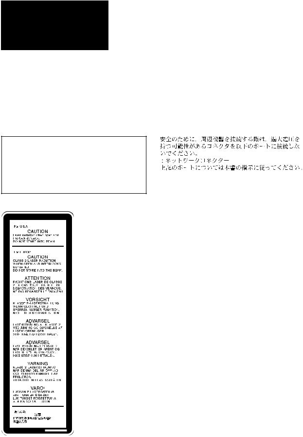
CLASS 1 LASER PRODUCT
LASER KLASSE 1 PRODUKT
LUOKAN 1 LASERLAITE
KLASS 1 LASER APPARAT
This Professional Disc Camcorder is classified as a CLASS 1 LASER PRODUCT.
Laser Diode Properties
Wavelength: 400 to 410 nm
Emission duration: Continuous
Laser output power: 135 mW (max. of pulse peak),
65 mW (max. of CW)
Standard: IEC60825-1 (2001)
GEFAHR
Bei geöffnetem Laufwerk und beschädigter oder deaktivierter Verriegelung tritt ein unsichtbarer Laserstrahl aus. Direkter Kontakt mit dem Laserstrahl ist unbedingt zu vermeiden.
This label is located insidethe outside panel of the unit.
CAUTION
The use of optical instruments with this product will increase eye hazard.
Use of controls or adjustments or performance of procedures other than those specified herein may result in hazardous radiation exposure.
X-RAY RADIATION WARNING
Be sure that parts replacement in the high voltage block and adjustments made to the high voltage circuits are carried out precisely in accordance with the procedures given in this manual.
For safety, do not connect the connector for peripheral device wiring that might have excessive voltage to the following port(s).
: Network connector
Follow the instructions for the above port(s).
2 (P) |
PDW-700/V1 (E) |
Table of Contents
Manual Structure |
|
1-9. Replacing the Flat Cables, Flexible Card |
|
||||
|
|
|
|
|
Wires/Boards ................................................................ |
1-45 |
|
Purpose of this manual ................................................................. |
5 |
1-10. Service Tools/Measuring Equipment List |
1-46 |
||||
|
|
|
|
||||
Related manuals ........................................................................... |
5 |
1-10-1. |
Service Tools ....................................................... |
1-46 |
|||
|
|
|
|
1-10-2. |
Measuring Equipment ......................................... |
1-47 |
|
1. |
Service Overview |
|
1-11. |
Firmware/Software ....................................................... |
1-48 |
||
|
1-11-1. |
EEPROM/FRAM List ......................................... |
1-48 |
||||
|
|
|
|
1-11-2. |
Firmware Update Using the USB Memory ......... |
1-49 |
|
1-1. Locations of Main Parts .................................................. |
1-1 |
1-11-3. |
Software Option Registration Method |
|
|||
1-1-1. |
Locations of the Printed Wiring Boards ................ |
1-1 |
|
|
by Using USB Memory ....................................... |
1-51 |
|
1-1-2. |
Locations of Main Mechanical Parts ..................... |
1-3 |
1-12. |
Other Overview |
1-52 |
||
|
|
|
|
||||
1-2. |
Circuit Description .......................................................... |
1-4 |
1-12-1. |
Notes on Handling Optical Block Assembly ...... |
1-52 |
||
1-2-1. |
Camera System ...................................................... |
1-4 |
1-12-2. |
Standard Torque for Screws ................................ |
1-53 |
||
1-2-2. |
CCD Block ............................................................ |
1-5 |
1-12-3. |
Stop Washer ........................................................ |
1-53 |
||
1-2-3. |
Video Signal System ............................................. |
1-5 |
1-12-4. |
Description of CCD Block Number .................... |
1-54 |
||
1-2-4. |
System Control ...................................................... |
1-6 |
1-12-5. |
Memory Backup Battery ..................................... |
1-54 |
||
1-2-5. |
Digital Audio System .......................................... |
1-12 |
1-12-6. |
IC Link Replacement .......................................... |
1-54 |
||
1-2-6. |
Audio System ...................................................... |
1-12 |
1-12-7. |
Circuit Protection Element .................................. |
1-54 |
||
1-2-7. |
Audio DSP Operation Processing ....................... |
1-14 |
1-12-8. |
Precautions for Use of Condensation Sensor ...... |
1-55 |
||
1-2-8. |
Optical Drive System .......................................... |
1-16 |
1-12-9. |
Precautions for the Battery Connector ................ |
1-55 |
||
1-2-9. |
Power Supply Systems ........................................ |
1-17 |
1-12-10. |
Notes on Repair Parts .......................................... |
1-55 |
||
1-2-10. |
LCD System ........................................................ |
1-18 |
1-12-11. |
Unleaded Solder .................................................. |
1-55 |
||
1-2-11. |
Others .................................................................. |
1-18 |
|
|
|
|
|
1-3. |
Matching Connectors .................................................... |
1-20 |
|
|
|
|
|
1-4. Signal Inputs and Outputs ............................................. |
1-20 |
2. |
XDCAM Web Site |
|
|||
1-5. |
On-Board Switch and LED Function ........................... |
1-24 |
|
|
|
|
|
1-6. How to Take Out a Cartridge Manually |
1-34 |
2-1. |
XDCAM Web Site Overview ......................................... |
2-1 |
|||
|
|
|
|
||||
1-6-1. |
Taking Out a Cartridge at Power-off ................... |
1-34 |
2-2. |
Status Menu .................................................................... |
2-3 |
||
1-6-2. |
When You Cannot Take Out a Cartridge Even |
|
2-2-1. |
Device Information ............................................... |
2-3 |
||
|
|
If Pressing the EJECT Button at Power-on ......... |
1-34 |
2-2-2. |
Hours Meter ........................................................... |
2-4 |
|
1-7. |
Removing/Installing |
1-35 |
2-2-3. |
Software Version ................................................... |
2-5 |
||
|
|
|
|
||||
1-7-1. |
Removing Outside Panel ..................................... |
1-35 |
2-3. |
Disc Menu ....................................................................... |
2-7 |
||
1-7-2. |
Reinstalling Outside Panel .................................. |
1-35 |
2-3-1. |
Disc Properties ...................................................... |
2-7 |
||
1-7-3. |
Inside Panel ......................................................... |
1-35 |
2-3-2. |
Thumbnails ............................................................ |
2-7 |
||
1-7-4. |
Handle Assembly ................................................ |
1-36 |
2-4. |
Maintenance Menu ......................................................... |
2-8 |
||
1-7-5. |
Front Panel .......................................................... |
1-37 |
2-4-1. |
Software Update .................................................... |
2-8 |
||
1-7-6. |
SW Guard Assembly ........................................... |
1-38 |
2-4-2. |
Account ............................................................... |
2-13 |
||
1-7-7. |
Shoulder Pad, Connector Cover .......................... |
1-38 |
2-4-3. |
Network ............................................................... |
2-14 |
||
1-7-8. |
Connector Panel Assembly ................................. |
1-39 |
2-4-4. |
License Registration ............................................ |
2-15 |
||
1-7-9. |
Rear Panel Assembly .......................................... |
1-40 |
|
|
|
|
|
1-7-10. |
Battery Connector ............................................... |
1-40 |
|
|
|
|
|
1-8. |
Removing/Installing LCD Block .................................. |
1-41 |
|
|
|
|
|
1-8-1. |
LCD Block .......................................................... |
1-41 |
|
|
|
|
|
1-8-2. |
LCD Hinge .......................................................... |
1-43 |
|
|
|
|
|
1-8-3. |
LCD Backlight and LCD Panel ........................... |
1-44 |
|
|
|
|
|
PDW-700/V1 (E) |
1 |
3. |
Error Messages |
|
|
3-1. |
Error Messages Overview ............................................... |
3-1 |
|
3-2. |
Error Code List ............................................................... |
3-2 |
|
3-2-1. |
Main Code and Sub Code ...................................... |
3-2 |
|
3-2-2. |
Error 0X ................................................................. |
3-3 |
|
3-2-3. |
Error 20 ................................................................. |
3-4 |
|
3-2-4. |
Error 3X ................................................................. |
3-5 |
|
3-2-5. |
Error 5X ................................................................. |
3-5 |
|
3-2-6. |
Error 6X ................................................................. |
3-5 |
|
3-2-7. |
Error 91 ................................................................. |
3-6 |
|
3-2-8. |
Error 92 ................................................................. |
3-7 |
|
3-2-9. |
Error 95 ................................................................. |
3-7 |
|
4. |
Setup Menu |
|
|
4-1. |
Setup Menus ................................................................... |
4-1 |
|
4-1-1. |
Basic Operations of Setup Menus ......................... |
4-1 |
|
4-1-2. |
How to Display the SERVICE Menu .................... |
4-1 |
|
4-2. |
TOP Menu ...................................................................... |
4-2 |
|
4-3. |
USER Menu .................................................................... |
4-3 |
|
4-4. |
OPERATION Menu ....................................................... |
4-4 |
|
4-5. |
PAINT Menu ................................................................ |
4-27 |
|
4-6. |
MAINTENANCE Menu ............................................... |
4-38 |
|
4-7. |
FILE Menu .................................................................... |
4-56 |
|
4-8. |
DIAGNOSIS Menu ...................................................... |
4-65 |
|
4-9. |
SERVICE Menu ........................................................... |
4-69 |
|
4-10. |
Drive Maintenance ........................................................ |
4-85 |
|
4-10-1. |
Basic Operation on Drive Maintenance |
|
|
|
|
Menus .................................................................. |
4-85 |
4-10-2. |
TEMPERATURE SENSOR ............................... |
4-85 |
|
4-10-3. |
DEW SENSOR ................................................... |
4-86 |
|
4-10-4. |
FAN MOTOR ..................................................... |
4-86 |
|
4-10-5. |
ACCELERATION SENSOR .............................. |
4-87 |
|
4-10-6. |
LOADER ............................................................. |
4-88 |
|
4-10-7. |
SLIDER-AUTO TEST ........................................ |
4-91 |
|
4-10-8. |
IN-LIM TEST ..................................................... |
4-91 |
|
4-10-9. |
OUT-LIM TEST ................................................. |
4-92 |
|
4-10-10. |
SPINDLE MOTOR-AUTO TEST ...................... |
4-92 |
|
4-10-11. |
FOCUS ACTUATOR ......................................... |
4-93 |
|
4-10-12. |
TRACKING ACTUATOR ................................. |
4-94 |
|
4-10-13. |
SA ACTUATOR ................................................. |
4-94 |
|
4-10-14. |
LASER ................................................................ |
4-95 |
|
4-10-15. |
ND FILTER ......................................................... |
4-95 |
|
4-10-16. |
SKEW .................................................................. |
4-96 |
|
4-10-17. |
LENS CLEANING ............................................. |
4-97 |
|
4-10-18. |
SERVO_1 ............................................................ |
4-97 |
|
4-10-19. SKEW .................................................................. |
4-97 |
||
4-10-20. SERVO_2 ............................................................ |
4-97 |
||
4-10-21. |
ACCELERATION OFFSET ............................... |
4-98 |
|
4-10-22. |
ERROR LOGGER .............................................. |
4-99 |
|
4-10-23. VERSION .......................................................... |
4-100 |
||
4-10-24. |
SERIAL NO ...................................................... |
4-100 |
|
4-10-25. |
CLEAR MEDIA LOG ...................................... |
4-100 |
|
4-10-26. UPLOAD TO EEPROM ................................... |
4-100 |
||
4-11. AUDIO A/D Error Correction .................................... |
4-101 |
||
4-12. AUDIO D/A Error Correction .................................... |
4-102 |
||
4-13. |
AUDIO LEVEL Volume Compensation .................... |
4-102 |
|
4-14. |
Adjusting Battery End Detection Voltage .................. |
4-103 |
|
4-15. |
SERVICE SUPPORT Menu ....................................... |
4-104 |
|
4-16. |
Setup Menu List .......................................................... |
4-105 |
|
5. |
File System |
|
|
5-1. Structure of File System ................................................. |
5-1 |
||
5-2. |
Data Structure ................................................................. |
5-2 |
|
5-3. |
Operating the Files and the Data Flow ........................... |
5-3 |
|
5-3-1. |
USER FILE ........................................................... |
5-3 |
|
5-3-2. |
ALL FILE .............................................................. |
5-5 |
|
5-3-3. |
REFERENCE FILE ............................................... |
5-7 |
|
5-3-4. |
Other FILE (SCENE FILE and LENS FILE) ....... |
5-9 |
|
5-3-5. |
SERVICE FILE ................................................... |
5-10 |
|
5-3-6. |
Other RESET ....................................................... |
5-11 |
|
5-4. |
Special Items to Save .................................................... |
5-12 |
|
5-4-1. |
White Gain .......................................................... |
5-12 |
|
5-4-2. |
Master Gain ......................................................... |
5-13 |
|
5-4-3. |
Shutter ................................................................. |
5-13 |
|
6. Periodic Maintenance and Inspection
6-1. Periodic Check/Replacement Parts List .......................... |
6-1 |
||
6-2. |
Cleaning .......................................................................... |
6-2 |
|
6-2-1. |
General Information for the Use of Cleaning |
|
|
|
|
Cloth ...................................................................... |
6-2 |
6-2-2. |
Cleaning Loader Assembly ................................... |
6-2 |
|
6-2-3. |
Cleaning Spindle Motor ........................................ |
6-3 |
|
6-2-4. |
Cleaning Pickup Lens ............................................ |
6-3 |
|
6-3. Cares after Using under Special Environment ................ |
6-4 |
||
6-4. |
Digital Hours Meter ........................................................ |
6-5 |
|
6-4-1. |
Display Method and Reset Methods ..................... |
6-5 |
|
6-5. |
Recommended Replacement Parts ................................. |
6-6 |
|
6-6. Precautions for the Battery Connector ............................ |
6-8 |
||
6-7. |
Precaution on Hanging Bracket of Handle ..................... |
6-8 |
|
2 |
PDW-700/V1 (E) |
7. |
Replacement of Main Parts |
|
7-8. Service Action After Replacing or Repairing |
|
|||
|
|
|
|
|
the Board ....................................................................... |
7-39 |
|
7-1. |
Optical Drive Assembly ................................................. |
7-1 |
7-8-1. |
Optical Block Assembly ...................................... |
7-39 |
||
7-1-1. |
Removing/Reinstalling Loader Assembly ............ |
7-1 |
7-8-2. |
AT-177 Board ..................................................... |
7-39 |
||
7-1-2. |
Removing/Reinstalling Drive Sub Assembly ....... |
7-5 |
7-8-3. |
CN-3005 Board ................................................... |
7-39 |
||
7-1-3. |
Replacing Cleaner Assembly ................................ |
7-7 |
7-8-4. |
DCP-44 Board ..................................................... |
7-39 |
||
7-1-4. |
Replacing Loading Motor Assembly .................... |
7-8 |
7-8-5. |
SY-355 Board ...................................................... |
7-40 |
||
7-1-5. |
Replacing Optical Block Assembly ...................... |
7-9 |
7-8-6. |
FP-157 Board ...................................................... |
7-40 |
||
7-1-6. |
Replacing No.2/No.3 Gear Assemblies ............... |
7-12 |
7-8-7. |
DR-606 Board ..................................................... |
7-40 |
||
7-1-7. |
Replacing Seek Motor Assembly ........................ |
7-14 |
7-8-8. |
SE-857 Board ...................................................... |
7-40 |
||
7-1-8. |
Replacing Spindle Motor .................................... |
7-15 |
|
|
|
|
|
7-1-9. |
Removing/Reinstalling Lock Release |
|
|
|
|
|
|
|
|
Assembly ............................................................. |
7-16 |
8. |
Optical Drive Alignment |
|
|
7-1-10. |
Removing/Reinstalling LD Motor ...................... |
7-17 |
|
|
|
|
|
7-2. Removing/Reinstalling Mounted Circuit Board of the |
|
8-1. Optical Drive Alignment Overview ................................ |
8-1 |
||||
|
Optical Drive ................................................................ |
7-18 |
8-1-1. |
Precautions ............................................................ |
8-1 |
||
7-2-1. |
SE-709 Board ..................................................... |
7-18 |
8-1-2. |
Fixtures .................................................................. |
8-1 |
||
7-2-2. |
SE-857 Board ..................................................... |
7-19 |
8-1-3. |
Preparations Before Adjustment ........................... |
8-1 |
||
7-2-3. |
SE-858 Board ..................................................... |
7-21 |
8-2. Procedures After Replacing the Optical Block |
|
|||
7-3. Replacing Fan Motor (Drive) ....................................... |
7-23 |
|
Assembly and the Board ................................................. |
8-1 |
|||
7-4. Replacing Fan Motor (Rear) ......................................... |
7-24 |
8-2-1. |
Adjustment After Replacing the Optical |
|
|||
7-5. |
Removing/Reinstalling CCD Unit ................................ |
7-25 |
|
|
Block Assembly .................................................... |
8-1 |
|
7-5-1. |
Removing CCD Unit ........................................... |
7-25 |
8-2-2. |
Adjustment After Replacing the DR-606 |
|
||
7-5-2. |
Reinstalling CCD Unit ........................................ |
7-26 |
|
|
Board ..................................................................... |
8-1 |
|
7-6. |
Service Action After Replacing the CCD Unit |
7-27 |
8-2-3. |
Adjustment After Replacing the SE-857 Board .... |
8-1 |
||
|
|
|
|
||||
7-7. |
Removing/Installing Boards |
7-28 |
8-3. |
Servo1 Automatic Adjustment ....................................... |
8-2 |
||
|
|
|
|
||||
7-7-1. |
CN-2947 Board and TG-260 Board .................... |
7-28 |
8-4. |
Skew Adjustment ............................................................ |
8-3 |
||
7-7-2. |
AT-177 Board and DCP-44 Board ...................... |
7-28 |
8-4-1. |
Tangential Skew Adjustment ................................ |
8-3 |
||
7-7-3. |
DVP-45 Board and SY-355 Board ...................... |
7-29 |
8-4-2. |
Radial Skew Adjustment ....................................... |
8-5 |
||
7-7-4. |
ENC-118 Board, HP-148 Board and |
|
8-5. |
Servo2 Automatic Adjustment ....................................... |
8-6 |
||
|
|
SW-1391 Board ................................................... |
7-29 |
8-6. |
Clearing Media Log ........................................................ |
8-6 |
|
7-7-5. |
FP-157 Board ...................................................... |
7-30 |
8-7. |
After Adjustment |
8-6 |
||
|
|
|
|
||||
7-7-6. |
CN-2946 Board and CN-3026 Board .................. |
7-31 |
|
|
|
|
|
7-7-7. |
KY-623 Board ..................................................... |
7-32 |
|
|
|
|
|
7-7-8. |
CN-3025 Board and SW-1425 Board ................. |
7-32 |
|
|
|
|
|
7-7-9. |
CN-3001 Board ................................................... |
7-33 |
|
|
|
|
|
7-7-10. |
IO-235 Board ....................................................... |
7-33 |
|
|
|
|
|
7-7-11. |
CI-37 Board ......................................................... |
7-33 |
|
|
|
|
|
7-7-12. |
PS-731 Board ...................................................... |
7-34 |
|
|
|
|
|
7-7-13. |
AXM-38 Board, CN-2948 Board, |
|
|
|
|
|
|
|
|
SW-1352 Board and RM-216 Board ................... |
7-34 |
|
|
|
|
7-7-14. |
MS-86 Board ....................................................... |
7-34 |
|
|
|
|
|
7-7-15. |
CNB-25 Board and PS-708 Board ...................... |
7-35 |
|
|
|
|
|
7-7-16. |
CN-3005 Board and SW-1426 Board ................. |
7-35 |
|
|
|
|
|
7-7-17. |
DR-606 Board ..................................................... |
7-36 |
|
|
|
|
|
7-7-18. |
RE-246 Board ...................................................... |
7-37 |
|
|
|
|
|
7-7-19. |
RX-101 Board ..................................................... |
7-37 |
|
|
|
|
|
7-7-20. |
MB-1111 Board ................................................... |
7-38 |
|
|
|
|
|
PDW-700/V1 (E) |
3 |
9. |
Electrical Alignment |
|
|
9-1. |
Preparation ...................................................................... |
9-1 |
|
9-1-1. |
Fixtures and Equipment ........................................ |
9-1 |
|
9-1-2. |
Connection ............................................................ |
9-1 |
|
9-1-3. |
Switch Setting before Adjustment ......................... |
9-2 |
|
9-1-4. |
Notes on Adjustment ............................................. |
9-2 |
|
9-1-5. |
Gray-Scale Chart and its Maintenance .................. |
9-3 |
|
9-2. |
Adjustment ...................................................................... |
9-4 |
|
9-2-1. |
Confirming VCO CONT Frequency ..................... |
9-4 |
|
9-2-2. |
Modulator Balance Adjustment ............................ |
9-4 |
|
9-2-3. |
VA Gain Adjustment ............................................. |
9-5 |
|
9-2-4. |
Black Shading Adjustment .................................... |
9-6 |
|
9-2-5. |
White Shading Adjustment ................................... |
9-7 |
|
9-2-6. |
Black Set Adjustment ............................................ |
9-8 |
|
9-2-7. |
Flare Adjustment ................................................... |
9-9 |
|
9-2-8. |
Auto Iris Adjustment ........................................... |
9-10 |
|
9-2-9. |
RPN Adjustment ................................................. |
9-11 |
|
9-2-10. |
S/H DC Adjustment ............................................ |
9-12 |
|
9-2-11. |
RPN Correction Procedure .................................. |
9-13 |
|
4 |
PDW-700/V1 (E) |

Manual Structure
Purpose of this manual
There are volume 1 and volume 2 in the Maintenance manual of PDW-700.
The maintenance manuals (volume 1, 2) are intended for use by trained system and service engineers, and provides the information of maintenance and detailed service.
Related manuals
The following manuals are available in this model.
If this manual is required, please contact your local Sony Sales Office/Service Center.
.Operation Manual (Supplied with the unit)
This manual is necessary for application and operation (and installation) of this unit.
.Maintenance Manual
Volume 1: Describes about maintenance information, parts replacement, and guideline for adjustment.
Part number: 9-968-417-03
Volume 2: Describes about block diagrams, schematic diagrams, board layouts and detailed parts list required for parts-level service.
Part number: 9-968-435-03
.“Semiconductor Pin Assignments” CD-ROM
This “Semiconductor Pin Assignments” CD-ROM allows you to search for semiconductors used in Broadcast and Professional equipment.
This manual contains a complete list of semiconductors and their ID Nos., and thus should be used together with the CD-ROM.
Part number: 9-968-546-06
PDW-700/V1 (E) |
5 |
Section 1
Service Overview
1-1. Locations of Main Parts
1-1-1. Locations of the Printed Wiring Boards
Main unit
@[
!\
$[
8
@\
$]
@'
!'
#' 


7
9
|
|
|
5 |
!; |
|
|
|
$= |
$\ |


@, |
@] |
|
$-
@/ !,
#[
#;
#]
@;
@=
!=
3
6
#.
#\
2
!]
1
!/
#-
!.
@-
!-
#=
1 AT-177 |
$- SW-1391 |
2 AXM-38 |
$= SW-1425 |
3 CI-37 |
$[ SW-1426 |
4 CN-2946 |
$] SY-355 |
5 CN-2947 |
$\ TG-260 |
6 CN-2948 |
|
7 CN-3001 |
|
8 CN-3005 |
|
9 CN-3025 |
|
0 CN-3026 |
|
!- CNB-25 |
|
!= DCP-44 |
|
![ DET-45 |
|
!] DET-47 |
|
!\ DR-606 |
|
!; DR-617 |
|
!' DVP-45 |
|
!, ENC-118 |
|
!. FP-157 |
|
@/ HP-148 |
|
@- HP-149 |
|
@= IO-235 |
|
@[ KY-623 |
|
@] LED-444 |
|
@\ MA-162 |
|
@; MB-1111 |
|
@' MS-86 |
|
@, PA-342/342A |
|
@. PA-343/343A |
|
#/ PA-344 |
|
#- PD-118 |
|
#= PS-708 |
|
#[ PS-731 |
|
#] RE-246 |
|
#\ RM-216 |
|
#; RX-101 |
|
#' SE-924 |
|
#, SW-1249 |
|
#. SW-1352 |
|
$/ SW-1385 |
|
PDW-700/V1 (E) |
1-1 |
Optical drive
4
2
1
3
1 SE-709
2 SE-857
3 SE-858
4 SW-1125G
1-2 |
PDW-700/V1 (E) |
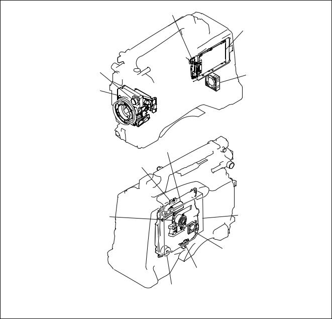
1-1-2. Locations of Main Mechanical Parts
3
4
2 |
5 |
|
|
1 |
|
9
!/

6
8
!=
1 CCD unit |
!- Optical block assembly |
2 Filter knob |
!= Seek motor assembly |
3 LCD Hinge assembly |
of the AT-177 board. The viewfinder uses the time data for displaying the time. The data for year, month, day, and time of the clock can be changed using the menu.
The settings for year, month, day, and time are sent to the FP_CPU and the year, month, day, and time are written to the Real Time Clock IC.
6.WARNING_LED control and alarm tone control The WARNING information is supplied from the ITRON
(CPU) that is used to turn on and off the WARNING LED on the FP-157 board.
The 1 KHz square wave generated from the PWM generator circuit inside the FP_CPU alarm tone is used as the alarm tone.
7.Wireless Receiver Control (Optional function)
This communication circuit can control both analog and digital wireless receivers.
Analog wireless receivers use the conventional method of synchronous serial communication (200 Bps).
(Interval time: 80 ms)
Digital wireless receivers use 38 KBps asynchronous serial communication to handle large amounts of communication data.
With a built-in wireless receiver, when FP_CPU is in the POWER-ON state, the receiver type is determined and information such as the transmission RF sensitivity is loaded. This data is transmitted to Camera CPU via ITRON (CPU) and can be viewed on the viewfinder.
8. Software download function
FP_CPU has internal flash memory so the software can be overwritten. Load the software in the memory stick into the camera microcomputer and transmit the data through ITRON (CPU) in the SY-335 board to the FP_CPU where it is written.
9. Power voltage measurement circuit (batteries other than the info battery)
Power voltage measurement circuit (IC839) outputs two types of DC voltage from DA output of the FP_CPU and switches voltage in the IC839 6-pin to switch between a measurement range of +9 V to +14 V and +12 V to +17 V. The voltage measurement is sent to ITRON (CPU) as the voltage value. ITRON calculates the remaining battery charge, creates voltage display data, and returns the data to FP_CPU. FP_CPU displays the voltage display data on the monochrome LCD. The voltage display data can be checked at the same time in the status menu for the color LCD.
|
CH1&2 |
|
|
|
|
|
|
|
|
|
|
|
|
IC705 |
|
|
|
|
|
|
|
|
|
|
|
|
|||||||||
|
or |
|
|
|
|
|
|
|
|
|
|
|
|
|
|
|
|
|
|
|
|
|
|
|
|
||||||||||
|
|
|
|
|
|
|
|
|
|
|
|
TC74HC4052 |
|
|
|
|
|
|
|
|
|
|
|
|
|||||||||||
|
CH3&4 |
|
|
|
|
|
|
|
|
|
|
|
|
|
|
|
|
|
|
|
|
|
|
|
|||||||||||
|
|
|
|
|
|
|
|
CH-1/3 |
|
|
|
|
|
|
|
|
IC706 |
|
|
|
|
|
|
|
|
|
|
|
|
||||||
|
CH-1/3 |
|
|
|
|
|
|
|
|
|
|
|
|
|
|
|
|
|
|
|
|
|
|
|
|
|
|
|
|||||||
|
|
|
|
|
|
|
|
|
|
|
|
|
|
|
|
|
|
|
|
|
|
|
|
|
|
|
|
|
|
|
|
||||
|
|
|
|
|
|
|
|
|
|
MIX |
|
|
|
|
|
|
|
|
|
NJM-2172 |
|
IC708 |
|
|
|
|
|
|
|
|
|
||||
|
|
|
|
|
|
|
|
|
|
|
|
|
|
|
|
|
|
|
|
|
|
|
|
|
|
|
|||||||||
|
|
|
|
|
|
|
|
|
|
|
|
|
|
|
|
|
|
|
|
|
|
|
|
|
|
|
|
|
|
|
|
||||
|
CH-2/4 |
|
|
|
|
|
|
|
|
|
|
|
|
|
|
|
|
|
|
|
VCA |
|
|
|
|
|
|
|
|
|
|
|
|||
|
|
|
|
|
|
|
|
CH-2/4 |
|
|
|
|
|
|
|
|
|
|
|
NJM386 |
|
Front_EARPHONE |
|||||||||||||
|
|
|
|
|
|
|
|
|
|
|
|
|
|
|
|
|
|
|
|
|
|
|
|||||||||||||
|
|
|
|
|
|
IC750 |
|
|
|
|
|
|
|
|
|
|
|
|
|
|
|
|
Final AMP |
|
|||||||||||
|
|
|
|
|
|
|
|
|
|
|
|
|
|
|
|
|
|
|
|
|
|
||||||||||||||
|
|
|
|
|
|
|
|
|
|
|
|
|
|
|
|
|
|
|
+InA OutA |
|
|
|
+ |
|
|
|
L |
|
|
|
|||||
|
FP-CPU |
|
|
|
MIX |
|
|
|
INV |
|
|
|
|
|
|
|
|
|
|
_InA |
|
|
_ |
|
|
|
R |
|
|
|
|
|
|
||
|
|
|
|
|
|
|
|
|
|
|
|
|
|
|
|
|
Cont |
|
|
|
|
CN701 |
|
|
|
|
|
|
|||||||
|
(CH-1/3, |
|
|
|
|
|
|
|
|
|
|
|
|
|
|
|
|
|
|
|
|
|
|
|
|
|
|
|
|
|
|
|
|
|
|
|
MIX, |
|
|
|
|
|
|
|
|
|
|
|
|
|
|
|
|
|
|
|
|
|
|
|
|
|
|
|
|
|
|
|
|
|
|
|
CH-2/4) |
|
|
|
|
|
|
|
|
IC704 |
|
|
|
|
|
|
|
|
|
|
|
|
|
|
|
|
|
|
|
|
|
|
|
||
|
|
|
|
|
|
|
|
|
|
|
|
|
|
|
|
|
|
IC707 |
|
IC709 |
|
|
REAR_EARPHONE |
||||||||||||
|
|
|
|
|
|
|
|
TC74HC4052 |
|
|
|
|
|
|
|
|
|
|
|
||||||||||||||||
|
|
|
|
|
|
|
|
|
|
|
|
|
|
|
|
NJM-2172 |
|
|
|
||||||||||||||||
|
|
|
|
|
|
|
|
|
|
|
|
|
|
|
|
|
|
|
|
|
|
NJM386 |
|
|
with SW |
||||||||||
|
|
|
|
|
|
|
|
|
|
|
|
|
|
|
|
|
|
|
|
|
|
|
|
|
|
|
|||||||||
|
|
|
|
|
|
|
|
|
|
|
|
|
|
|
|
|
|
|
|
|
|
|
|
Final AMP |
|
|
|
|
|
|
|
|
|
||
|
|
|
|
|
|
|
|
|
|
|
|
|
|
|
|
|
|
|
|
|
|
|
|
|
|
|
|
|
|
|
|
|
|||
Mono |
OutB |
|
+ |
|
|
CN702 |
SW |
|
CH-1/3 |
+InB |
|
_ |
|
|
L |
|
|
_InB |
|
|
|
|
|
|||
Streo |
|
|
|
|
|
|
|
|
VCA |
|
IC710 |
|
|
|
|
||
|
|
|
R |
|
|
|||
|
|
|
NJM386 |
|
|
|
||
|
|
|
Final AMP |
|
|
|
|
|
SW |
OutA |
|
+ |
|
|
|
|
|
|
+InA |
|
_ |
|
|
|
SW |
|
|
_InA |
IC706 |
|
|
|
|
|
|
|
|
|
|
|
|
|
||
|
Cont |
VCA |
|
|
FP_CPU |
|
|
CN703 |
|
|
|
|
|
|
|
||
Mono |
+3 Vdc |
|
+3 Vdc |
(SP ATT LEVEL:0dB) |
|
|
||
+InA OutB |
|
|
|
Q712 |
|
|
||
|
|
|
|
|
|
|||
|
|
|
|
|
Q715 |
|
MONITOR |
|
CH-2/4 |
RV700 |
_InA |
|
|
FP_CPU |
SW-1 |
||
|
|
|
||||||
|
|
|
|
|
|
|
SP |
|
Streo |
|
Cont |
|
|
(SP ATT LEVEL:_3dB) |
|
||
|
|
|
|
|
||||
|
MONITOR-VR |
|
|
RV701 |
|
Q711 |
|
|
|
ALARM-VR |
FP_CPU |
Q716 |
SW-2 |
|
|||
|
|
|
|
|
||||
FP-CPU(Head Phone Out:Streo/Mono) |
|
|
|
|
(SP ATT LEVEL:_6dB) |
|
|
|
|
ALARM SIGNAL(FP_CPU) |
|
|
|
Q713 |
|
|
|
|
|
|
FP_CPU |
Q717 |
SW-3 |
|
||
|
FP_CPU (MIN ALARM VOL) |
|
R761 |
|
|
|||
|
|
(SP ATT LEVEL:_9dB) |
|
|
||||
|
|
|
|
|
|
|
||
|
|
Q707 |
|
|
|
Q718 |
|
|
|
|
|
|
|
|
|
SW-4 |
|
|
When ALARM-VOL Position 0 %, |
|
|
|
|
|||
|
Alarm Level is about _38 dBu. |
|
|
|
|
|||
Audio Monitor Block
1-8 |
PDW-700/V1 (E) |
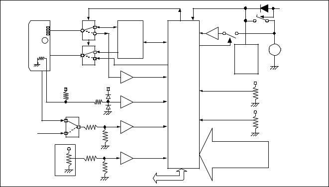
10. Info battery communication circuit.
This equipment supports batteries with SM Bus specifications. The serial communication bus (SDA, SCL) for IC916 (Parallel bus to I2C_bus Controller) connected to the FP_CPU bus passes through IC927 and IC928 (switching switch) and connects to the serial terminal of the info battery. The Serial Clock Rate is 88 KHz.
The battery type, remaining time, and other information is loaded onto FP_CPU and transmitted to ITRON (CPU). ITRON (CPU) calculates the remaining battery charge and creates remaining charge display data, and transmits the data to Camera CPU and FP_CPU. FP_CPU displays the remaining charge display data on the monochrome LCD. The remaining charge display data can be checked at the same time in the status menu for the color LCD.
11. Power off software control circuit
FP_CPU detects the POWER-SW OFF information. When power can be turned on, the "Power OFF" command is sent from ITRON (CPU) and FP_CPU controls the power OFF circuit on the CNB-25 board.
12. FP_CPU backup circuit
Even when power is turned off for FP_CPU, the data is saved for the internal RAM and Real Time Clock (RX8025NB) through backup on a coin battery. By saving the system data, FP_CPU can be started up quickly when the power is turned on.
13.Backup lithium battery voltage measurement circuit FP_CPU performs voltage measurement on the backup lithium battery. When recharging is detected, the reducedvoltage information is send to ITRON (CPU). (Measurement interval time: 60 s)
Current is prevented from running through FET-SW (Q836) in order to prevent power from being lost during measurement. Furthermore, reverse current above +3 V is prevented with FET-SW (Q829), thus extending the life of the lithium battery. The battery life is guaranteed for about
5years.
14.FP_CPU independent operations
When the POWER-SW is set to power off, power is supplied from the UNSW +12 V power circuit to display the counter and other information on the monochrome LCD. Power is supplied to each power regulator with IC830 (hyposaturation regulator 8 V) and independent operations can be performed. The operations can be turned on or off from the menu.
15. REAR input control
The serial communication bus (SDA, SCL) for IC917 (Parallel bus to I2C_bus Controller) connected to the FP_CPU bus sends control for the AXM-38 board through the motherboard with IC202 (PCA-9555: I2C_I/O_PORT) on the CNB-25 board and acquires the following information: REAR_XLR automatic insertion detection
|
|
|
|
|
|
|
|
|
|
|
+3 V |
+3 V |
|
|
|
IC927 |
|
|
|
|
|
|
|
|
|
BATTERY |
|
|
IC916 |
|
|
|
|
|
|
(IC805) |
||
SW |
|
IC928 |
|
|
|
|
|
|
|
|||
|
PCA9564 |
|
|
|
|
|
|
Q829 |
||||
|
|
|
|
|
|
|
|
Q836 |
||||
|
INFO_ BATT |
|
I2C_BUS |
|
|
|
|
|
|
|||
F |
A |
|
|
|
Port |
Vcc |
IC844 |
FET-SW |
||||
_SDA |
|
SDA |
|
|
FET-SW |
|||||||
|
|
|
|
8 bit |
|
|
|
|
||||
E |
|
|
|
|
|
AN15 |
|
|
|
|
||
|
B |
|
|
|
CPU_BUS |
|
|
|
|
|||
|
|
|
|
D7 |
D15 |
|
|
|
|
|
||
|
|
|
|
|
|
|
|
|
|
|
||
|
|
|
|
|
: |
|
: |
Port |
|
|
|
Lithium |
Battery |
INFO_BATT |
A |
|
|
D0 |
|
D8 |
(1 time/60 sec) |
IC908 |
Coin |
||
|
SCL |
|
|
IC921 |
|
Battery |
||||||
ID Register |
_SCL |
|
|
|
|
|
|
|
Real Time |
|||
|
|
|
|
|
HD64F2378 |
|
|
+3 V |
||||
|
|
|
|
|
|
|
|
|
||||
|
|
B |
|
|
|
|
CPU |
|
|
|
Clock |
|
|
|
|
|
|
|
|
|
|
|
|||
+ |
|
|
|
IC914 |
|
Voltage |
Port |
|
CLOCK 16 MHz |
RX-8025NB |
|
|
|
|
|
|
|
|
|
|
|
|
|||
|
|
|
|
|
measurement |
AN11 |
|
|
|
|
|
|
|
|
|
|
|
|
|
|
|
|
|
|
|
|
+3 V |
|
+3 V |
|
|
|
|
|
|
|
+3 V |
|
|
|
|
|
|
|
|
Voltage measurement |
|
||||
|
|
|
|
|
|
|
|
AN8 |
|
|||
|
Battery |
|
IC838 |
|
Voltage |
|
|
|
CH-1 |
|
||
|
|
|
|
|
|
|
RV1 |
|
||||
|
ID Data |
|
|
measurement |
|
|
|
|
|
|||
|
|
|
AN14 |
|
|
|
|
|
||||
|
|
|
|
|
|
|
|
|
|
|
|
|
|
FET-SW |
|
|
|
|
|
|
|
|
|
+3 V |
|
|
(CNB-25 board) |
|
|
|
|
|
|
|
|
|
|
|
|
|
|
IC839 |
|
|
|
|
Voltage measurement |
|
|||
|
|
UNREG+12 V |
|
Voltage |
|
AN9 |
|
|||||
Battery-in |
|
|
|
|
|
|
CH-2 |
|
||||
|
|
|
|
measurement |
AN13 |
|
|
|
|
|||
|
|
|
|
|
|
|
RV2 |
|
||||
|
|
|
|
|
|
|
|
|
|
|
||
|
|
|
|
|
|
|
|
AN0 |
|
|
|
|
|
|
|
|
|
|
|
|
|
|
|
|
|
DC-in |
|
|
|
|
|
|
|
AN1 |
|
|
|
|
|
|
|
|
|
|
|
|
AN2 |
FRONT,REA,WRR-SW1,2,3,4 |
|
||
|
|
|
|
|
|
|
|
AN3 |
|
|||
|
+5 V |
|
|
IC7 |
|
|
|
|
CTL,TC,U_BIT-SW |
|
||
|
|
|
|
Voltage |
|
AN4 |
|
|
||||
|
|
|
|
|
|
|
|
FREE,SET,REC_RUN-SW |
|
|||
Front |
|
|
|
|
measurement |
AN10 |
AN5 |
PRESET,REGENE,CLOCK-SW |
|
|||
Microphone |
|
|
|
|
|
|
AN6 |
|
|
Monitor-SW |
|
|
|
|
|
|
|
|
|
|
|
|
|||
Volume |
|
|
|
|
|
|
|
AN7 |
|
(3 digitize level) |
|
|
|
SW-1425 |
|
|
to iTRON_CPU |
|
|
|
|
|
|
||
|
|
|
|
|
|
|
|
|
|
|
|
|
Voltage Measurement Block Overview
PDW-700/V1 (E) |
1-9 |
circuit control, microphone amplifier gain control, operational amplifier power control, and digital/analog input switching switch information.
16.REAR XLR automatic insertion detection circuit control (DET-47 board and sensor holder)
Combine the DET-47 board on the sensor holder and connect with the harness to the AXM-38 board.
The infrared light emitter uses one LED that connects to the CH1 and CH2 receivers positioned in the middle of the sensor holder on the left and right sides. When “Detection ON” is set from the menu and the XLR connector is inserted into the 3P-XLR connector, the infrared light is blocked, the output from the receivers changes from L to H, and insertion is detected. At this time, CH1 and CH2 operate automatically and the XLR input on the REAR area is selected. (CH3 and CH4 are not switched automatically. ) Detection interval time is 200 ms.
17. Color LCD monitor drive control and opening/rotation detection circuit
The CN108 connector is connected to the power supply and the RGB signal for video, the passes through CN802 to connect directly into the LCD driver.
FP_CPU and LCD driver are connected with synchronous serial communication. During POWER_ON, parameters
such as brightness and contrast can be set. This information is saved in the LCD (PD-118 board) nonvolatile memory and the FP-157 board IC913 (nonvolatile memory).
Rotation is detected by the rotation sensor switch in DET45 after passing through CN802.
Opening and closing is detected from the hole terminal (H801) on the FP-157 board and the field intensity from the permanent magnet (neodymium: Ne-FeB).
18. Nonvolatile memory control
IC907 on the FP-157 board is nonvolatile memory that supports the I2C bus.
This memory stores system information such as the A/D and D/A error compensation values and color LCD settings. During POWER-ON, this information is sent to ITRON (CPU) and the color LCD device.
19. Monochrome LCD display circuit with backlight FP_CPU and IC806 (UPD7225GB) are connected by a 500 KHz serial communication port. IC806 is an LCD controller/driver that is programmable with software. ND800 displays the BATTERY value, DISC capacity, time, and counter value on the monochrome LCD at three hour intervals.
H_AMP12CH_ON |
L_A/D_PD12CH_ON |
|
|
FP_H_AUOUT_ON FP_H_AUIN_ON |
||
|
B1 |
DVP-45 board |
|
|
B3 |
B4 |
|
|
|
|
CNB-25 board |
|
|
|
|
|
|
|
|
|
|
|
PD |
|
AMP |
ch1 |
|
Buffer |
|
|
|
|
||
ch1 |
AK5383 |
AK4382 |
ch1 |
|
|
|
ATT |
|
|
|
|
||
|
|
|
FIL |
|
|
|
|
|
|
|
|
|
|
|
|
|
|
TER |
|
|
|
|
|
|
AMP |
|
|
Buffer |
ch2 |
|
|
ch2 |
ch2 |
|
ATT |
|
|
|
|||
|
|
|
|
|
||
|
|
|
|
|
|
|
|
AMP |
|
|
AMP |
|
|
|
|
|
|
Monitor-OUT |
AXM-34 board |
|
|
AMP |
AK5383 |
|
|
|
|
Buffer |
|
|
|
|
||
ch3 |
|
|
STEREO |
|
||
ATT |
|
|
REAR-1 |
|||
|
|
|
|
|
||
|
|
|
|
|
(-3,0,4 dB standard ATT) |
|
Buffer |
ch4 |
|
|
|
|
REAR-2 |
ATT |
|
|
MONO |
|
||
|
PD |
|
|
|||
|
AMP |
|
MIX/CH1/CH2 |
|
|
|
|
FP-157 board |
|
|
|
||
|
|
|
|
|
||
|
B2 |
|
|
MA-162 board |
RX-101 board |
|
H_AMP34CH_ON |
L_A/D_PD34CH_ON |
|
|
|||
|
|
|
|
|||
|
|
|
|
FrontMIC-1 |
|
|
|
|
|
|
FrontMIC-2 |
|
|
Audio Power Save Block
1-10 |
PDW-700/V1 (E) |

|
PCA-9555-4 |
I/OIN&OUT +3V |
AXM-38 |
AudioinSelectSw AmpGainControl |
DET-47 |
XLR-DETCT |
SW-1352 |
SW-1 SW-2 |
|
|
|
|
|
|
CNB-25 |
I2C-BUS(+3V) |
|
|
|
|
|
|
|
|
|
|
|
|
|
I2C-BUS(+5V) |
|
|
|
|
|
|
Magnet |
45 |
LCD Position |
COLOR-LCD |
(CXD-3662R) |
KY-623 |
PCA-9555-3 I/OOUT+3V |
I2C-BUS(+3V) |
|
FET SW N Channel |
|
|
|
AntonSW |
I2CBUS(88KHz) CONTROL-2 IC916(PAC9564) |
|
|
BusSw |
SCK3,TxD3, RxD3 |
DVP-45
8bit |
PORT |
|
SY-355
CPU iTRON
CPU |
Camera |
|
|
|
|
|
|
|
|
|
AT-177 |
|
|
|
|
|
|
|
|
|
MENU STBY/SAVE OFF/ONLOW/M/HIGH PREST DDC- |
DCP-44 |
MB-1111 |
MA-162 MIC-AMP GAINControl |
CN-3001 |
MIC 5Pterminal |
SW-1425 |
FRONT MIC |
ENC-82 |
Rotary |
SW-1391 |
Audio System Control
PDW-700/V1 (E) |
1-11 |
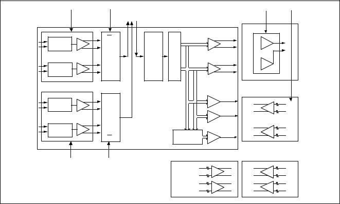
1-2-5. Digital Audio System
DVP-45 board
1. Audio signal processing system <Recording system>
The analog audio signal input from the AUDIO IN connector is converted into a serial digital audio signal (two channels) with the AUDIO A/D converter on the FP157 board. The digital audio signal enters CAVA (IC200) of the DVP-45 board through the MB-1111 board.
The serial digital audio signal (four channels) input from the AES/EBU INPUT connector undergoes level conversion in the AXM-38 board and is input into CAVA (IC200) of the DVP-45 board. After the signal is decoded in CAVA (IC200), it is synchronized and converted to the same sampling rated as the recorded video signal with the sampling rate converter (IC700, IC703).
Digital audio signals (eight channels) that include input HD-SDI signal (when the option is attached) are decoded with the DCP-44 board. Then, the signals are converted into serial digital audio signals and entered into CAVA (IC200) of the DVP-45 board via the MB-1111 board. CAVA (IC200) selects the above entered digital audio signal and sends it as the recorded audio data to AUDIO REC DSP (IC800).
<Playback system>
The playback digital audio signal that underwent playback signal processing in AUDIO PB DSP (IC801) is entered into CAVA (IC200), then separated and converted into the serial digital audio signals for analog output systems and digital output systems.
The analog output system serial digital audio signal is sent to the AUDIO D/A converter in the FP-157 board via the MB-1111 board. After it is converted into an analog audio signal, the signal is output to the AUDIO OUT connector, headphone, and monitor speaker.
The digital output system serial digital audio signal is sent to the DCP-44 board via the MB-1111 board. The signal is combined with the video signal in the DCP-44 board and output as the HD/SD-SDI audio signal.
2. Digital signal processing system <Recording system>
The recording audio data from CAVA (IC200) undergoes signal processing such as recording level control, muting process, and MIX/SWAP in AUDIO REC DSP (IC800), and then it is sent to PIER G4 (IC1900) as recording digital audio data.
1-12
The recording digital audio data is sent to AUDIO Low Resolution DSP (IC900) through CAVA (IC200), Proxy audio data is generated in compressed A-Low format, and the data is sent to PIER G4 (IC1900).
The above recording digital audio data and recording compressed Proxy audio data are written PIER_SDRAM (IC1901 to IC1904).
The recording digital data from the i.LINK/network is sent to PIER G4 (IC1900) via the PCI bus and written to the PIER_SDRAM (IC1901 to IC1904).
While recording to a disc, the data in PIER_SDRAM (IC1901 to IC1904) is sent to the DR-606 board via the ATA interface.
<Playback system>
The audio data and the Proxy audio data are sent to PIER G4 (IC1900) via the ATA interface and written to the PIER_SDRAM (IC1901 to IC1904).
The playback digital audio data in PIER_SDRAM (IC1901 to IC1904) is sent from PIER G4 (IC1900) to AUDIO PB DSP (IC801), After performing signal processing such as limiter, playback level control, and mute processing, the signal is input to CAVA (IC200).
The audio data and Proxy audio data in PIER_SDRAM (IC1901 to IC1904) is provided to i.LINK/network via the PCI bus as the MXF file data.
3. Sync signal system
The reference signal is always the 24.576 MHz clock entered from the DCP-44 board, whether recording or playing back.
This reference clock is divided and timing signal for 256 FS, 64 FS and FS audio processing is generated.
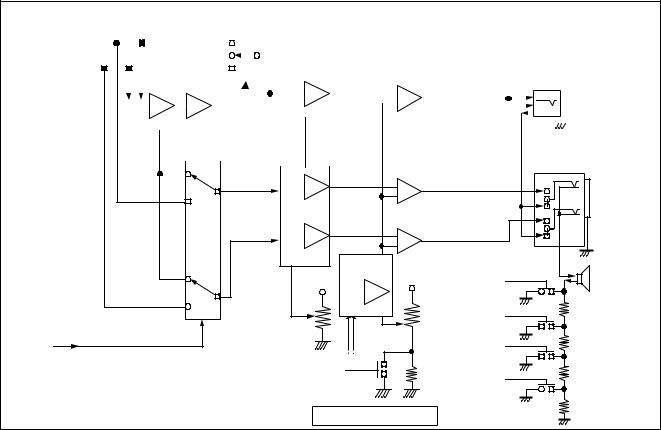
1-2-6. Audio System
Block structure |
|
Front microphone amp |
: MA-162 board |
Input signal selector |
: FP-157 board |
A/D circuit (CH1&2) |
: FP-157 board |
A/D circuit (CH3&4) |
: FP-157 board |
D/A circuit |
: FP-157 board |
Final amp |
: CNB-25 board |
Monitor amp |
: FP-157 board |
Rear input |
: AXM-38 board |
DPS operation processing |
: DVP-45 board |
PDW-700/V1 (E)
1. Front microphone amp
The front microphone amp on the MA-162 board comes with a gain switch. (30 dB/20 dB/10 dB)
Gain switching can be performed from the menu. (_60 dBu/_50 dBu/_40 dBu)
2. Input signal selector
The audio signal can be selected with the analog switch (IC1 to IC4) based on the side panel switch information.
3. A/D circuit
A/D uses 24-bit AK-5383. The sampling frequency is 48 KHz.
The first has an ATT circuit for head room level adjustment.
4. D/A circuit
D/A uses 24-bit AK-4382A. The sampling frequency is 48 KHz.
The latter has a differential LPF circuit and an output level amp circuit.
5. Final amp
The final amp is located on the CNB-25 board and is connected to the AXM-38 board with the connector-to- connector. The CH1 and CH2 output signals are output from the 5-pin XLR connector.
The output level can be selected as _3 dBu, 0 dBu, or +4 dBu from the menu.
6. Monitor amp
Composed of the monaural amp for the front earphone and stereo amp for the rear earphone, the volume control is
performed with the operational amp with electronic volume (NJM2172).
7. Rear input
The rear input is composed of the following: a switch for Line In, AES/EBU, and MIC-IN; +48 V ON/OFF-SW; automatic detection circuit (DET-47 board) for the 3-pin input XLR connector; and the microphone amp (10 dB/20 dB/30 dB).
Gain switching can be performed from the menu. (_60 dBu/_50 dBu/_40 dBu)
Line In input level setting can be switched to +4 dBu, 0 dBu, or _3 dBu with the slide switch on the AXM-38 board. (Open the inside panel.)
Operation description
After the power to the device is turned on, each port in the FP-157 board CPU is initialized, the necessary resistor data is set, and MUTE is cancelled. (After approximately 3 seconds, the digital EE sound can be monitored.)
The front mic signal passes through the MA-162 board and MB-1111 board before entering the input signal selector (analog switch: IC1 to IC4) of the FP157 board.
The rear input signal passes through the AXM-38 board, CNB-25 board, and MB-1111 board before entering the input signal selector (analog switch: IC1 to IC4) of the FP157 board.
The information from the FRONT/REAR/WIRELSS switch position can be obtained by loading the three
Fs |
|
|
|
|
|
|
Fs |
|
64Fs |
|
|
|
|
|
|
64Fs |
|
|
23 |
0 |
|
23 |
0 |
|
|
|
A/D OUT CH3&4 (24bit) |
MSB |
|
CH3 MSB |
|
|
CH4 |
AN34 |
|
|
23 |
0 |
CH1 MSB |
23 |
0 |
|
|
|
A/D OUT CH1&2 (24bit) |
MSB |
|
|
|
CH2 |
AN12 |
DVP-45 |
|
(Left Justified,24bit Data) |
|
|
|
|
|
|
|
|
|
|
|
|
|
|
|
|
|
|
23 |
0 |
CH3 MSB |
23 |
0 |
|
|
|
D/A IN CH3&4 (24bit) |
MSB |
|
|
|
CH4 |
DA34 |
|
|
|
|
|
|
|
|
|
||
D/A IN CH1&2 (24bit) |
MSB 23 |
0 |
CH1 MSB |
23 |
0 |
CH2 |
DA12 |
|
|
|
|
|
|
|
|
||
(Left Justified,24bit Data) |
|
32bit |
|
|
32bit |
|
|
|
|
|
|
|
|
|
|
A/D & D/A Signal Format Diagram
PDW-700/V1 (E) |
1-13 |
signals from the switch connected to each A/D terminal in the FP_CPU (S1 to S4).
FP_CPU sends the switch position information to ITORN_CPU of the SY-355 board, and then selects the audio signal by receiving the audio mode information from the ITORN_CPU.
The selected CH1 and CH2 system signals enter the differential amp (IC5: balance-to-unbalance converter) and pass through the head room level switching circuit and balance-to-unbalance conversion amp for A/D. Then, the signals are applied to the A/D converter IC (IC102: 24-bit). The serial digital audio signal (2 channels) converted to digital is entered to VAX (IC200) of the DVP-45 board via the MB-1111 board
VAX (IC400) selects the entered digital audio signal and sends it as the recorded audio data to AUDIO REC DSP (IC800).
DSP for audio performs high-speed processing for operations such as gain processing during manual operations, AUTO processing, LIMITER processing, 67 Hz notch filter while using the front mic, LPF (15 KHz) ON/OFF, internal SG, and audio level detection.
On the other hand, the front volume and side volume are connected to the A/D terminal in the CPU and the volume voltage is converted into digital with the internal 10-bit A/ D. After being converted into a multiplication value for DSP, the signal is sent to ITORN_CPU.
ITORN_CPU performs operation processing on the
combined front and side volumes and sends the results to DSP.
The D/A serial signal for playback passes through the DVP-45 board and MB-1111 board and enters the digital switch (IC461) of the FP-157 board. In the monitor CHSW, CH1&2 or CH3&4 is selected and applied to the 24bit D/A converter (IC453).
The D/A converter output passes through the differential LPF, ATT balance-to-unbalance conversion amp (IC514), and MB-1111 board. It is applied to the final amp (IC200, IC201) of the CNB-25 board and output from the 5-pin XLR connector (AXM-38 board).
The audio signal for the monitor passes from IC520/620 output through the monaural, mix, and stereo switching switch (IC703, IC704). Then, the signal is applied to the operation amp (NJM2172) with electronic volume.
The rear earphone can be switched between stereo and mono from the menu.
The monitor speaker output level can be lowered from the volume. Select one of the following for the ATT value: 0, _3 dB, _6 dB, or _9 dB.
1-2-7. Audio DSP Operation Processing
Main functions
1.AUTO-AMP: Two to four types of characteristics can be selected depending on each headroom.
InPut
24dBu
20dBu
10dBu
+4dBu +0dBu _3dBu
_10dBu
_20dBu
_30dBu
_40dBu
_50dBu
_60dBu
Digital_WRR; |
I2S-Format |
DSP |
|
_20dBFS |
AES/EBU; |
|
Reference OUT : _40dBFS |
|
|
||||
_40dBFS |
|
(TMS320DA150GGU120) |
|
|
Reference OUT : _20dBFS |
|
(DSP setting the same MIC |
|
|
|
|||
|
|
|
|
|
|
|
as specifications) |
|
|
|
|
|
|
XLR-OUT
|
|
|
|
16dB:ATT 4dB |
|
|
20dBFS |
|
|
|
|
HeadRoom |
|
|
|
|
|
|
|
12dB:ATT 0dB |
|
|
|
|
_ |
_ |
|
18dB:ATT 6dB |
|
|
|
_ |
20dB |
24dB |
|
20dB:ATT 8dB |
|
|
|
17dB |
|
|
|
30dB |
40dB |
|
|
|
|
|
|
|
|||
|
|
|
_20dBu |
Tp-1 |
AK5383 |
||
|
|
|
|
_21dBu |
|
|
24bit |
|
|
|
|
|
|
A/D |
|
|
|
|
|
|
|
Tp-101 |
|
WireLess |
_30dBu |
|
|
_30dBFS |
|||
_31dBu |
|
_29dBu |
|||||
|
|
|
|
|
|||
|
|
|
|
|
|
|
|
|
_40dBu |
MIC |
|
|
_39dBu |
_40dBFS |
|
|
|
Max Input : 0dBu |
|
||||
|
|
|
|
|
|||
_50dBu |
Max Input : _10dBu |
|
|
|
|||
|
|
|
|
|
|||
_60dBu |
|
|
|
|
LINE-IN; |
||
|
|
|
|
HeadRoom : Get 30dBu |
|||
|
Max Input : _20dBu |
|
|||||
|
|
AK-5383 input : _23dBu |
|||||
|
|
|
|
|
|
||
|
|
|
|
|
|
(X, Y terminal : _29dBu) |
|
|
|
|
|
|
|
MIC-IN; |
|
|
|
|
|
|
|
HeadRoom : Get 40dBu |
|
|
|
|
|
|
|
AK-5383 input : _33dBu |
|
|
|
|
|
|
|
(X, Y terminal : _39dBu) |
|
ALARM-TONE
|
|
CPU_OUT:2.7dBu |
||||||||
|
|
|
|
|
|
|
|
|
|
|
_4dBu |
|
|
_ |
|
|
|||||
|
|
|
||||||||
_8dBu |
|
|
17 |
|
||||||
|
|
|
. |
|
||||||
_10dBu |
|
|
|
|
|
5dB |
Tp-500 |
|||
|
|
|||||||||
|
|
|
|
|
|
|
|
|||
_12dBu |
|
|
|
|
|
|
|
|
|
|
|
|
_3dB |
_15dBu |
|||||||
AK4382A |
|
|
||||||||
|
|
|
|
|
|
|
|
|
|
|
24bit |
|
|
|
|
HeadRoom |
|||||
D/A |
|
|
|
|
_12dB:ATT8dB |
|||||
|
|
|
|
|
_16dB:ATT4dB |
|||||
|
|
|
|
|
_18dB:ATT2dB |
|||||
|
|
|
|
|
_20dB:ATT0dB |
|||||
|
|
(Controled ATT of DAC) |
||||||||
|
|
|
|
|
|
|
|
|
|
|
AK-4382A |
|
|
|
|
|
|
|
|
|
|
Max Output; |
|
|||||||||
±2.75Vp-p |
|
|
|
|
|
|
|
|
|
|
+5dBu |
|
|
|
|
|
|
|
|
+9dBu |
(IN : +24dBu, Limiter-ON) |
|||||||
|
|
|
|
|
|
|
|
+4dBu |
|
|
|
|
|
|
|||
|
|
|
|
|
|
|
|
|
|
|
|
|
|
|
|
||
|
|
|
|
|
|
|
|
|
|
+0dBu |
(IN : +4dBu, AGC-ON) |
||||||
20dB |
|
|
|
|
|
|
|
|
|
_3dBu |
|
|
|
|
|
|
|
|
|
|
|
|
|
|
|
|
|
|
|
|
|
|
|
|
|
|
|
9dB |
|
|
Tp-501 |
|
|
_4dBu |
|||||||||
|
|
|
|
|
|
|
|||||||||||
|
|
+ |
|
|
_10dBu |
|
|
26dB |
|
|
|
|
|
|
|||
|
_ |
|
|
14dB |
|
|
|
|
|
|
HeadPhone |
|
|
||||
|
|
|
|
|
|
|
|
|
|
|
|
|
|
|
_13dBu |
|
|
_ |
_ |
|
+ |
|
|
|
|
|
|
|
|
|
||||
|
|
|
|
|
+ |
|
_22dBu (8Z loded) |
|||||||||
|
12dB |
9dB |
|
|
|
|||||||||||
15dB |
|
|
|
|
|
|
|
|
|
|
|
|
|
|||
|
|
|
|
|
|
|
|
|
|
|
|
|
||||
|
|
|
|
|
|
|
|
|
|
|
|
|
|
|
|
|
|
|
|
|
|
|
|
|
|
|
|
|
|
|
|
|
|
|
|
|
|
|
|
|
|
|
|
|
|
|
|
|
|
|
_ |
|
|
|
VR_Max:_30dBu |
|
26dB |
|
|
_31dBu |
|
|
|||||
33dB |
+ |
|
|
ALARM (Max) |
||||||||||||
|
|
|
|
|
|
|
|
|||||||||
|
|
|
|
|
|
|
|
|
|
|
|
|
|
|
|
|
|
|
|
|
VR_Max:_48dBu |
|
|
|
|
|
|
|
|||||
|
|
|
|
|
|
|
|
|
|
|
||||||
|
|
|
|
|
|
|
|
|
|
|
26dB |
|
|
_62dBu |
|
|
|
|
|
|
|
|
|
|
|
|
+ |
|
ALARM (Min) |
||||
|
|
|
|
|
|
|
|
|
|
|
|
|
Faint : On |
|||
|
|
|
|
|
|
|
ALARM_VR(Min):Faint_On |
|
|
|
|
|
|
|
||
|
|
|
|
|
|
|
|
|
|
|
|
|
|
|||
|
|
|
|
|
|
|
|
|
|
|
26dB |
|
|
_90dBu |
|
|
|
|
|
|
|
|
|
|
|
|
+ |
|
ALARM (Min) |
||||
|
|
|
|
|
|
|
|
|
|
|
|
|
Faint : Off |
|||
ALARM_VR(Min):Faint_Off
Audio Level Chart
1-14 |
PDW-700/V1 (E) |
2.LIMITER characteristics: Two to four types of characteristics can be selected depending on each headroom.
3.OUT_PUT_LIMITER characteristics: Performs LIMITER processing on the PB and EE_OUT. ON/ OFF.
4.Turns on and off the HPF (67 Hz) and LPF (15 KHz; _24 dB). (Runs automatically during front microphone selection)
5.Performs gain control when CH1 and CH2 are on MANUAL status. (VR-MAX: +12 dB)
6.CH3 and CH4 turn on and off the AUTO operation.
7.Internal SG: Four types of 1 KHz/_12, _16, _18, _20 dBFS.
8.Recording error correction: +0 to _2 dB (started from the terminal)
9.Playback error correction: +0 to _2 dB (started from the terminal)
10.INPUT delay amount: Performs delay processing to match the VIDEO and AUDIO phases of each CH.
Description of each part
1.DIGITAL AUTO_AMP Processing Selects the AUTO level from the menu.
AU AUTO SPEC : _6 dB/_9 dB/_12 dB/_15 dB/_17 dB _6 dB : Linear operation until approx. _9 dBFS. Approx.
_6 dBFS at Max.
_9 dB : Linear operation until approx. _12 dBFS. Approx. _9 dBFS at Max.
_12 dB : Linear operation until approx. _15 dBFS. Approx. _12 dBFS at Max.
_15 dB : Linear operation until approx. _18 dBFS. Approx. _15 dBFS at Max.
_17 dB : Linear operation until approx. _20 dBFS. Approx. _17 dBFS at Max.
2.DIGITAL In Put LIMITER characteristics (only during MANUAL)
Selects the LIMITER level from the menu.
AU AUTO SPEC : _6 dB/_9 dB /_12 dB/_15 dB/_17 dB
_6 dB |
: Linear operation until approx. _9 dBFS. Approx. |
|
_6 dBFS at Max. |
_9 dB |
: Linear operation until approx. _12 dBFS. |
|
Approx. _9 dBFS at Max. |
_12 dB : Linear operation until approx. _15 dBFS. Approx. _12 dBFS at Max.
_15 dB : Linear operation until approx. _18 dBFS. Approx. _15 dBFS at Max.
_17 dB : Linear operation until approx. _20 dBFS. Approx. _17 dBFS at Max.
PDW-700/V1 (E)
|
|
|
|
|
: Features in common of the MIC/LINE input. |
|||||||
0 |
|
|
|
|
|
|
|
Features of the AGC/LIM OFF. |
||||
|
|
|
|
|
|
|
|
|
|
|
|
|
|
_6dBFS |
|
|
_5.4dBFS max |
|
|
|
|
|
|
||
|
|
|
|
|
|
|
|
|
|
|
|
|
_10 |
_9dBFS |
|
|
|
|
|
|
|
|
|
|
|
_12dBFS |
|
|
|
|
|
|
|
|
|
|
|
|
|
|
|
|
|
|
|
|
|
|
|
|
|
|
_15dBFS |
|
|
|
|
|
|
|
|
|
|
|
_20 |
_17dBFS |
|
|
|
|
|
|
|
|
|
|
|
Output level at 0dBFS input. |
|
|
|
|
|
|
|
|
|
|||
|
|
|
|
|
|
|
|
|
|
|||
_30 |
|
|
|
|
_8.4dBFS max |
|
|
|
|
|||
|
|
|
|
|
|
|
|
|
|
|
|
|
|
|
|
|
|
_11.4dBFS max |
|
|
|
||||
_40 |
|
|
|
|
|
_14.4dBFS max |
|
|
|
|||
|
|
|
|
|
_16.4dBFS max |
|
|
|
||||
|
|
|
|
|
|
|
|
|
||||
_50 |
|
|
|
|
|
|
|
_4.8dBFS max |
|
|
||
|
|
|
|
|
|
|
_7.8dBFS max |
|
|
|||
[dBFS] |
|
|
|
|
Subthresholdlevel |
17.9dBFS |
dBFS20.0 |
|
|
|||
|
|
|
|
dBFS14.6 |
dBFS11.4 dBFS8.1 |
0dBFS |
|
|
||||
_60 |
|
|
|
|
|
|
|
|
_10.8dBFS max |
|
||
|
|
|
|
|
|
|
|
|
_13.8dBFS max |
|
||
_70 |
|
|
|
|
|
|
|
|
|
_15.8dBFS max |
||
|
|
|
|
|
|
|
|
|
|
|
|
|
OUTOPUT |
_70 |
_60 |
_50 |
_40 |
_30 |
_20 |
_10 |
0 |
+10 |
+20 |
||
|
||||||||||||
|
|
|
|
INPUT [dBFS] |
|
|
Max input level |
|
|
|||
|
|
|
|
|
|
|
|
|
|
|
||
|
|
|
|
|
|
|
|
|
of the LINE input. |
|
||
|
|
|
|
|
|
|
|
|
|
|
Max input level |
|
|
|
|
|
|
|
|
|
|
|
|
of the MIC input. |
|
AGC/LIM SPECIFICATION
3. DIGITAL Out Put LIMITER characteristics Turn the LIMITER ON/OFF from the menu.
ON : Linear operation until approx. _12 dBFS, approx. _11 dBFS (at Max.)
OFF : Turn off LIMITER at 0 dBFS.
4. Gain control during MANUAL
The A/D converted VR value is converted into a DSP multiplication value at FP_CPU and synchronized with the VIDEO1 frame, then handed over to the CPU to set in the register of the DSP. The maximum variable for volume is +12 dB. (_∞ to +12 dB)
5. Recording error correction
For error correction on the A/D converter for audio, the multiplication value is corrected in the range +0 to _2 dB. Starts from the terminal with the standard signal level applied. (fully automatic)
6. Playback error correction
For error correction on the D/A converter for audio, the multiplication value is corrected in the range +0 to _2 dB. The correction is performed after the playback error correction is completed. Starts from the terminal. (semiautomatic)
The internal SG is used as the standard signal, and the inside panel for each LEVEL_VR is turned and fine-tuned.
1-15
1-2-8. Optical Drive System
Recording System
Recording data sent from the DVP-45 board through the ATA bus (Ultra ATA33) is sent to the Blu-ray Disc Controller (BDC) IC300 on the DR-606 board.
The BDC performs signal processing to conform to recording format, such as ATA interface, ECC coding and 17PP (Parity Preserve/Prohibit RMTR) modulation.
The recording data is converted to multi-pulse in the BDC, and the multi-pulse data is sent through the flexible card wire to the optical block to be written into the disc.
Playback System
•Data Playback System
The RF signal played back from the disc is sent from the optical block to the Front End Processor (FEP) IC200 on the DR-606 board where equalizing and asymmetry correction are performed after the RF signal passes through the AGC. After A/D conversion by the read clock played back in the PLL, the signal is sent to the BDC IC300.
In the BDC, the signal passes through the adaptive digital filter, and Viterbi demodulation, 17PP demodulation, and ECC decoding are applied to the signal. Then the signal is sent through the ATA bus to the DVP-45 board as played back data.
•Address restoration system
The address data restored from the disc is sent from the optical block to the FEP (IC200) on the DR-606 board. The analog address data passes through the AGC and BPF and is converted to digital data in the FEP. The digital data is then sent to the BDC (IC300) for address decoding.
The PLL in the FEP generates a wobble clock (WCK).
Servo System
•Tri-Axis Actuator and SA Actuator
The object lens of the optical block is controlled for focus direction, track direction, and tilt angle by the tri axis actuator.
The light reflected from the disc is converted to the electrical signal by the optical block. The electrical signal is input to the FEP IC200, and the focus error signal and the track error signal are detected. The SV DSP IC400 outputs the control data based on the errors to the driver IC501 and controls the focus actuator and the track actuator through the driver.
The tilt actuator is controlled for its angle against the disc to be optimum based on the tilt adjustment result for the jitter of the playback signal to be minimum and the output of the angular velocity sensor.
The SA actuator position is controlled for the spherical aberration to be optimum at the start-up adjustment when the disc is inserted. The SA actuator for the double layer disc is controlled to the optimum position every time to jump the layer.
•Seek Motor
The seek motor controls the position of the optical block so that the track to be recorded or played back is kept within the object lens driving range.
•ND Filter
The transmission factor of the ND filter is selectable to reduce the laser noise that occurs when the read power light is emitted for the single layer disc.
•Spindle Motor
The FG generated by the spindle motor is amplified and shaped on the SE-857 board, and is then input into the SV DSP IC400 on the DR-606 board.
The SV DSP compares the FG frequency with the target frequency, and then controls the spindle motor via the driver IC500.
System Control
The SY CPU IC600 on the DR-606 board performs system control. It controls ATA interface, Data Manager, RFrelated ICs, servo ICs, and loader. It also carries out interlocking control, maintenance and error log management of each device including the optical block. Firmware programs of the SY CPU and DSP as well as sources of each PLD are stored in the flash memory IC602, and the CPU loads them to each device when the power is turned on.
The BDC IC300 and SV DSP IC400 are controlled by the parallel CPU bus, while RF-related ICs are controlled by the serial port through SYS PE IC700.
Adjustment values and hours meter data are stored in the EEPROM IC4 on the SE-857 board.
1-16 |
PDW-700/V1 (E) |
1-2-9. Power Supply Systems
CNB-25 board
The board checks the input voltage +12 V, and controls distribution of the input power to each circuit board.
•Power ON/OFF Control
The ON/OFF control is performed in IC1 and IC5. The IC1 input signals include L PWR SW ON signal, H POWERW HOLD signal, EXTDC detection signal, battery detection, excess voltage detection, and low voltage detection. During normal operation, when L PWR SW ON signal is turned to “L”, Q4, 5, 6, and 7 or Q11, 12, 15, and 16 are turned on, and the battery or EXT DC IN +12 V is supplied to respective circuit. The H POWERW HOLD signal is sent from the FP-157 board after the main power of this unit is turned on. Therefore, the power is kept on even if the L PWR SW ON (L) signal is set to OFF (H). In order to turn off the main power of this unit, the L PWR SW must be turned off (H) and the H POWERW HOLD signal must be opened and set to “L”. When the FP-157 board detects that the POWER switch is turned OFF, it sets the POWERW HOLD signal to “L” to turn off the power after a disc operation is completed if the equipment is in the midst of operating a disc.
•Battery/EXT DC selector
The EXT DC voltage is detected and either battery or EXT DC is selected with priority given to the EXT DC. The IC5 performs the control and Q4, Q5, Q6, and Q7 are turned on when a battery is selected and Q11, Q12, Q15, and Q16 are turned on when the EXT DC is selected.
In this IC5, a step-up circuit (Vcc +8.5 V) that drives the N-CH MOS FET gate is employed.
•Protection from Excess Input Voltage
VOLTAGE DETECT (IC18) monitors the input +12 V. If the voltage exceeds approximately +18 V, the output of the IC18-1 is set to “H”. This is input to IC1 to start the protection from the excess voltage and turn on the +12 V output. (SHUT DOWN)
Since this function is a latch operation, the main power of the unit needs to be turned off once and back on after
the input power is set to below 18 V.
•Excess current detection
The output circuit of the UNREG +12 V has excess current detection resistors R70, R71 and R72. A voltage drop at the resistors is detected by the IC5.
When the voltage drop at the resistors exceeds 200 mV, the +12 V output is turned off.(SHUT DOWN) Another SHUT DOWN signal is the H SHUT DOWN
signal that is supplied from the RE-246 board. If any one of the DC-DC converter outputs is shorted, the output 12 V enters the SHUT DOWN state except UN SW +12 V. (SHUT DOWN)
Since this function is a latch operation, the main power of the unit needs to be turned off once and back on after the cause of the excess current is removed.
•Protection against input power connection of reverse polarity
If the input power is connected in reverse polarity, FET (Q2) is turned off so that the GND lines of the control system circuits are disconnected. Thus the control circuits are protected and supply of +12 V power to the respective circuits is stopped.
•FAN voltage control
The Q13 and Q14 are controlled by the FAN CONT signal from the AT-177 board and the PWM wave is converted to the DC voltage according to the DUTY.
The voltage controls the FAN and reduces the temperature increase.
•Audio Circuit
This is the output circuit for the AUDIO OUT (rear connector). The signal is output by selecting the CH1/2 or CH3/4 in the MONITOR.
•± 4.8 regulator circuit
This is the voltage regulator for AUDIO using on the AXM-38 board.
PDW-700/V1 (E) |
1-17 |
1-2-10. LCD System
PD-118 board
The PD-118 board consists of the color LCD panel drive circuit and the power supply circuit for LCD backlight. IC1 is the color LCD panel drive IC that contains of the built-in video signal RGB driver, the timing generator, and the VCO.
IC1 also contains the serial interface circuit and electronic potentiometers that are used to establish the various setups in accordance with the commands from the microprocessor (IC921) of the FP-157 board.
The RGB video signals that are input to IC1 pin-37 through pin-39 receive contrast adjustment and brightness adjustment. Then, they pass through the output signal polarity inversion circuit and are output from IC1 pin-20 through pin-22.
The factory adjustment data is stored in the IC3 EEPROM. The respective timing signals for driving the LCD panel are generated from the sync signals that are input to IC1 pin-41 and pin-42.
The operations such as turning off the backlight and inverting the video signal left to right or up to down are performed in accordance with the control signals supplied from the microprocessor (IC921) of the FP-157 board.
1-2-11. Others
CN-3005 board
The VF power supply, light power supply, light switch signal, and the EEPROM circuit that stores the rely and system information of the handle switch signal are included.
Handle switch relay
Input and output the handle switch signal (CN2).
Light switch relay
Relays the light switch signal (CN3).
EEPROM
The system information is written to the EEPROM (IC2) by the I2C communication to control.
MS-86 board
The MS-86 board is the connector board for the memory stick connection.
When a memory stick is inserted, the INS signal is set to
LOW so that the camera microprocessor checks capacity and types of the memory stick inserted.
VCC is supplied to a memory stick only when a memory stick is inserted or only when accessing a file on a memory stick. When VCC is supplied, the INS_LED and ACTIVE_LED (D1) is turned ON.
Access to the memory stick data is processed in the following order: VCC IN → SCLK ON → BS Pulse → DATA IN/OUT → SCLK OFF → . . → SCLK ON → BS ON → DATA IN/OUT → SCLK OFF → . . → VCC OFF.
1-18 |
PDW-700/V1 (E) |
AXM-38 |
XLR5P OUT |
4dB |
4dB |
CNB-25 |
|
|
|
|
|
|
|
PB 4ch |
4ch |
ResoLow 4ch |
|
|
|
|
|
|
|
|
|
||
|
|
|
|
|
|
|
|
PB |
|
|
Rec4ch |
|
|
|
|
|
|
|
DE MUX |
|
DE MUX |
|
|
|
|
|
|
|
|
|
4ch |
|
|
DE MUX |
|
DigitalOUTD12 |
DigitalOUTD34 |
ANAOUTD12 |
ANAOUTD34 |
|
32BITx |
|
|
|
EE |
PB |
|
|
|
DSP(120MHz) TM320DA150GG120 |
4ch REC |
|
|
|
|
PB |
|
|
|
|
32BITx |
|
|
|
|
|
|
|
|
VAX |
|
|
|
|
|
24bit I2S |
Left Justified 24bit |
DataCnv. |
|
CAD12 |
CAD34 |
AES/EBUD12 |
AES/EBUD34 |
AUD12 |
AUD34 |
DigitalWRRD12 |
DigitalWRRD34 |
|
|
|
|
|
SRC |
|
|
|
|
|
|
DVP-45 |
|
|
|
|
|
|
|
|
MB-1111 |
|
|
|
|
|
|
|
|
|
|
|
|
|
|
FRONT |
HeadPhone |
MONITORSP |
|
|
|
|
|
|
|
|
|
|
|
|
|
|
|
|
|
|
|
REAR |
Stereo HeadPhone |
|
|
|
|
|
|
|
|
|
|
|
|
|
|
|
|
|
|
||||||
|
|
|
|
|
|
|
|
|
|
|
|
|
|
|
|
|
NJM |
368M |
|
|
|
|
|
|
|
|
|
NJM 368M |
|
|
NJM |
368M |
|
|
|
|
|
|
|
|
|
||||||||||||||||||||
|
|
|
|
|
|
|
|
|
|
|
|
|
|
|
|
|
|
|
& |
|
|
|
|
15dB |
|
|
|
|
|
|
|
|
|
|
|
|
|
|
|
|
|
|
|
|
|
|
|
|
|
|
|
|
|
|
ATT |
|
33dB |
|
|||
|
|
|
|
|
|
|
|
|
|
|
|
|
|
|
|
|
|
|
|
|
|
|
|
|
|
|
|
|
|
|
|
|
|
|
|
|
|
|
|
|
|
|
|
|
|
|
|
|
|
|
|
|
|
|
|
||||||
|
|
|
|
|
|
|
|
|
|
|
|
|
|
|
|
|
|
|
|
|
ATT |
|
|
|
|
|
|
|
|
|
|
ATT |
|
15dB |
|
|
|
ATT |
|
15dB |
|
|
|
|
|
|
|
|
|
|
|
|
|||||||||
|
|
14dB |
|
|
|
|
|
|
14dB |
|
|
|
|
|
|
|
|
|
|
|
|
|
|
|
|
|
|
|
|
|
|
|
|
|
|
|
ControlControl-VR |
|
|
NJM |
2172 |
|
VCA 95dB |
||||||||||||||||||
|
|
|
|
|
|
|
|
|
|
|
|
|
|
|
|
|
|
|
|
|
|
|
|
|
|
|
|
|
|
|
|
|
|
|
|
|
|
||||||||||||||||||||||||
|
|
|
|
|
|
|
|
|
|
|
|
|
|
|
|
|
|
|
|
|
|
|
|
|
|
|
|
|
|
|
|
|
|
|
|
|
|
|
|
|
|
|
|
|
|
|
|
||||||||||||||
|
|
|
|
|
|
|
|
|
|
|
|
|
|
|
|
|
|
|
|
|
|
|
|
|
|
|
|
|
|
|
|
|
|
|
|
|
|
|
|
|
|
|
|
|
|
||||||||||||||||
|
ATT |
0dB |
9dB |
|
12dB 0dB 3dBATT 0dB |
|
9dB |
12dB |
|
|
|
|
|
|
NJM |
|
SW VCA 95dB |
|
|
|
|
|
|
|
|
|
|
NJM |
SW VCA 95dB |
|
|
|
|
|
|
15dBu ATT |
17.5dB |
|
|
Control-VR |
|||||||||||||||||||||
|
|
|
+4dB |
|
|
|
|
|
|
|
|
|
|
|
|
|
|
|
|
|
2172 |
|
|
|
|
|
|
|
|
|
|
|
|
|
|
|
|
2172 |
|
|
|
|
|
|
|
|
|
|
|
|
|
|
|
|
|
|
|
|
|||
|
|
|
|
|
|
|
|
|
|
|
|
|
|
|
|
|
|
|
|
|
|
|
|
|
|
|
|
|
|
|
|
|
|
|
|
|
|
|
|
|
|
|
|
|
|
|
|
|
|
|
|
|
|
|
|
||||||
|
|
|
|
|
|
|
|
|
|
|
|
|
|
|
|
|
|
|
|
|
|
|
|
|
|
|
|
|
|
|
|
|
|
|
|
|
|
|
|
|
|
|
|
|
|
|
|
|
|
|
|
|
|
|
|
|
|
|
|
|
|
|
|
|
|
|
|
|
|
|
|
|
|
|
|
|
|
|
|
|
|
|
|
|
|
|
|
|
|
|
|
|
|
|
|
|
|
|
|
|
|
|
|
|
|
|
|
|
|
|
|
|
|
|
|
|
|
|
|
|
|
|
|
|
|
|
|
|
|
|
|
|
|
|
|
|
|
|
|
|
|
|
|
|
|
|
|
|
|
|
|
|
|
|
|
|
|
|
|
|
|
|
|
|
|
|
|
|
|
|
|
|
|
|
|
|
|
|
|
|
|
|
|
|
|
|
|
|
|
|
|
|
|
|
|
|
|
|
|
|
|
|
|
|
|
|
|
|
|
|
|
|
|
|
|
|
|
|
|
|
|
|
|
|
|
|
|
|
|
|
|
|
|
|
|
|
|
|
|
|
|
|
|
|
|
|
|
|
|
|
|
|
|
|
|
|
|
|
|
|
|
|
|
|
|
|
|
|
|
|
|
|
|
|
|
|
|
|
|
|
|
|
|
|
|
|
|
|
|
|
|
|
|
|
|
|
|
|
|
|
|
|
|
|
|
|
|
|
|
|
|
|
|
|
|
|
|
|
|
|
|
|
|
|
|
|
|
|
|
|
|
|
|
|
|
|
|
|
|
|
|
|
|
|
|
|
|
|
|
|
|
|
|
|
|
|
|
|
|
|
|
|
|
|
|
|
|
|
|
|
|
|
|
|
|
|
|
|
|
|
|
|
|
|
|
|
|
|
|
|
|
|
|
|
|
|
|
|
|
|
|
|
|
|
|
|
|
|
|
|
|
|
|
|
|
|
|
|
|
|
|
|
|
|
|
|
|
|
|
|
|
|
|
|
|
|
|
|
|
|
|
|
|
|
|
|
|
|
|
|
|
|
|
CH1 |
|
|
+ |
|
|
|
|
|
|
|
|
|
|
|
CH1 |
|
|
|
|
|
|
CH2 |
|
|
|
|
|
|
|
|
|
|
|
|
|
|
|
|
|||
|
|
|
|
|
|
|
|
|
|
|
|
|
|
|
|
|
|
|
|
|
|
|
|
|
|
|
|
|
|
|
|
|
|
|
|
|
|
|
|
|
|
|
|
|
|
|
|
|
|
|
|
|
|
|
|||||||
|
|
|
|
|
|
|
|
|
|
|
|
|
|
|
|
|
|
|
|
|
|
|
CH2 |
|
|
|
|
|
|
|
|
|
|
|
|
|
|
|
|
|
|
|
|
|
|
|
|
|
|
|
|
|
|
|
|||||||
|
CH1: 15dBu |
|
|
|
|
|
CH2: 15dBu |
|
|
|
|
|
|
|
|
|
|
|
|
|
|
|
|
|
|
|
|
|
|
|
|
|
|
|
|
|
|
|
|
|
|
|
|
|
|
|
|
|
|
|
|
|
|
|
|
|
|
|
|
|
|
|
|
|
|
|
|
|
|
|
|
|
|
|
|
|
|
|
|
|
|
|
|
|
|
|
|
|
|
|
|
|
|
|
|
|
|
|
|
|
|
|
|
|
|
|
|
|
|
|
|
|
|
|
|
|
|
|
|
||||
|
|
|
|
|
|
|
|
|
|
|
|
|
|
|
|
|
|
|
|
|
|
|
|
|
|
|
|
Control |
|
|
|
|
|
|
|
|
|
|
|
|
|
|
|
|
|
|
|
|
|
|
|
|
|
|
|
|
|||||
|
|
|
|
|
|
|
|
|
|
|
|
|
|
|
|
Control |
|
|
|
|
|
|
|
|
|
|
|
|
|
|
|
|
|
|
ALARM-TONE |
|
|
|
|
|
|
|
|
|
|
|
|
|
|
|
|
|
|
||||||||
|
|
0dB |
|
|
|
|
|
|
0dB |
|
|
|
|
|
|
|
|
|
|
|
|
|
|
(ControledATTofDAC) |
|
|
|
|
|
|
|
|
|
|
|
|
|
|
|
|
|
|
|
|
|
PCA9555 |
|
|
|
|
|
|
|
|
|||||||
|
|
|
|
|
|
|
|
|
|
|
|
|
|
|
|
|
|
|
|
|
|
|
|
|
|
|
|
|
|
|
|
|
|
|
|
|
|
|
|
|
|
|
|
|
|
|
|
|
|
|
|
||||||||||
|
|
|
|
|
|
|
|
|
|
|
|
|
|
|
12dB:ATT8dB |
16dB:ATT4dB |
|
18dB:ATT2dB |
20dB:ATT0dB |
|
|
|
|
|
|
|
|
|
|
|
|
|
|
|
|
|
|
|
|
|
|
|
|
|
|
|
|
|
|||||||||||||
|
|
3dB |
LPF |
|
|
|
|
|
3dB |
|
LPF |
|
|
|
|
|
|
HeadRoom |
|
|
|
|
|
|
|
|
|
|
|
|
|
|
|
|
|
|
|
|
|
|
|
|
|
|
|
|
|
|
|||||||||||||
|
|
|
|
|
|
|
|
|
|
|
|
|
|
|
|
|
|
|
|
|
|
|
|
|
|
|
|
|
|
|
|
|
|
|
|
|
|
|
|
|
|||||||||||||||||||||
|
|
|
|
|
|
|
|
|
|
|
|
|
|
|
|
|
|
|
|
|
|
|
|
|
|
|
|
|
|
|
|
|
|
|
|
|
|
|
|
|
|
||||||||||||||||||||
|
|
|
|
|
|
|
|
|
|
|
|
|
|
|
|
|
|
|
|
|
|
|
|
|
|
|
|
|
|
|
|
|
|
|
|
|
|
|
|
|
|
|
|
||||||||||||||||||
|
|
|
|
|
|
|
|
|
|
|
|
|
|
|
|
|
|
|
|
|
|
|
|
|
|
|
|
|
|
|
|
|
|
|
|
|
|
|
|
|
|
|
|
|
|
|
|||||||||||||||
|
|
|
|
|
|
|
|
|
|
|
|
|
|
|
HaedRoom ATT |
|
|
|
|
|
|
|
|
|
|
|
|
|
|
|
|
|
|
|
|
|
|
|
FPCPU HD64F2378 |
|
|
|
|
|
|
|
|
|
|
|
|
|
|
|
|
|
|
||||
|
X |
Y |
AK-4382A 24bitD/A X |
|
|
|
Y |
|
|
|
Control |
|
|
|
|
|
|
|
|
|
|
|
|
|
|
|
|
|
|
|
|
|
PCA9564 |
I2CBUS |
|
|
|
|
|
|
|||||||||||||||||||||
|
|
|
|
|
|
|
|
|
|
|
|
|
|
|
|
|
|
|
|
|
|
|
|
|
|
|
|
|
|
|
|
|
|
|
|
|
|
|
|
||||||||||||||||||||||
|
|
|
|
|
|
|
|
|
|
|
|
|
|
|
|
|
|
|
|
|
|
|
|
|
|
|
|
|
|
|
|
|
|
|
|
|
|
|
|
|
|
|
|
|
|
|
|
|
|
|
|
|
|||||||||
|
|
|
|
|
|
|
|
|
|
|
|
|
|
|
|
|
|
|
|
|
|
|
|
|
|
|
|
|
|
|
|
|
|
|
|
|
|
|
|
|
|
|
|
|
|
|
|
|
|
|
|
|
|
|
|
|
|
|
|
|
|
|
|
|
|
|
|
|
|
|
|
|
|
|
|
|
|
|
|
|
|
|
|
Control |
|
|
|
|
|
|
|
|
|
|
|
|
|
|
|
|
|
|
|
|
|
|
|
|
|
|
|
|
|
|
|
|
|
|
|
|
|
||
|
|
|
|
|
|
|
SW |
|
|
|
|
|
|
|
|
|
|
|
|
|
|
|
|
|
|
|
|
|
|
|
|
|
|
|
|
|
|
SystemControl |
|
|
|
|
|
|
|
|
|
|
|
|
|
|
|
|
|
|
|||||
|
|
|
|
|
|
|
|
|
|
|
|
|
|
|
|
|
|
|
|
|
|
|
|
|
|
|
|
|
|
|
|
|
|
|
|
|
|
|
|
|
|
|
|
|
|
|
|
|
|
|
|
|
|
|
|||||||
|
|
|
|
|
|
|
|
|
|
|
|
|
|
|
|
|
|
|
|
|
|
|
|
|
|
|
|
|
|
|
|
|
|
|
|
|
|
|
|
|
|
|
|
|
|
|
|
|
|
|
PCA9555 |
|
|
|
|
|
|
||||
|
|
|
|
|
|
|
|
|
|
|
|
|
|
|
|
|
|
|
|
|
|
|
|
|
|
|
|
|
|
|
|
|
|
|
|
|
|
|
|
|
|
|
|
|
|
|
|
|
|
|
|
|
|
|
|
|
|||||
|
|
|
|
|
|
|
|
|
|
|
|
|
|
|
|
|
|
|
|
|
|
|
|
|
|
|
|
|
|
|
|
|
|
|
|
|
|
|
|
|
|
|
|
|
|
|
|
|
|
|
|
|
|
|
|
|
|||||
|
|
|
|
|
|
|
|
|
|
|
|
|
|
|
|
|
|
|
|
|
|
|
|
|
|
|
|
|
|
|
|
|
|
|
|
|
|
|
|
|
|
|
|
|
|
|
|
|
|
|
|
|
|
|
|
|
|||||
|
|
|
|
AK-5383 |
24bitA/D |
|
X |
Y |
|
|
|
|
|
|
|
AK-5383 |
24bitA/D |
|
|
X |
|
Y |
|
|
|
|
|
|
|
Audio |
|
|
|
|
|
|
|
|
|
|
|
|
|
|
|
|
|
|
|||||||||||||
|
|
|
|
|
Tp101 |
Tp201 |
|
|
|
0dB |
|
|
|
|
|
|
|
|
|
|
Tp301 |
Tp401 |
|
|
|
|
0dB |
|
|
|
|
|
|
|
|
|
|
|
|
|
|
|
|
|
|
|
|
|
|
|
|
|
|
|
|
||||||
|
|
|
|
|
|
|
|
|
|
|
|
|
|
|
|
|
|
|
|
|
|
|
|
|
|
|
|
|
|
|
|
|
|
|
|
|
|
|
|
|
|
|
|
|
|
|
|
|
|
||||||||||||
|
|
|
|
|
|
|
|
|
|
|
|
|
|
|
|
|
|
|
|
|
|
|
|
|
|
|
|
|
|
|
|
|
|
|
|
|
|
|
|
|
|
|
|
|
|
|
|
|
|||||||||||||
|
|
|
|
|
|
|
|
|
|
|
|
|
|
|
|
|
|
|
|
|
|
|
|
|
|
|
|
|
|
|
|
|
|
|
|
|
|
|
|
|
|
|
|
|
|
|
|
|
|
|
|
|
|
||||||||
|
|
|
|
|
|
|
|
|
|
|
|
|
|
|
|
|
|
|
|
|
|
|
|
|
|
|
|
|
|
|
|
|
|
|
|
|
|
|
|
|
|
|
|
|
|
|
|
|
|
|
|
||||||||||
|
|
|
|
|
|
|
HeadRoom |
|
|
|
|
|
|
|
|
|
|
|
|
|
|
|
|
|
|
|
|
|
|
|
|
|
|
|
|
|
|
|
|
|
|
|
|
|
|
|
|
|
|
|
|
||||||||||
|
|
|
|
|
|
|
|
|
|
|
|
SW |
|
|
|
|
|
Control |
|
|
|
|
|
|
|
|
|
|
HeadRoom SW |
|
|
|
|
Control |
(Balanced/Unbalanced) |
|
|
|
|
|
|
|
|
|
|
|
|
|
|
|
|
|
|
|
|
||||||
|
|
|
|
|
Tp1 |
Tp2 |
|
|
|
|
|
|
|
|
|
|
|
|
|
|
Tp3 |
Tp4 |
|
|
|
|
|
|
|
|
|
|
|
DifferentialAmplifier |
|
|
|
|
|
|
|
|
|
|
|
Control |
|
|
|
|
|
|
|||||||||
|
|
|
|
|
|
|
|
|
|
|
|
|
|
|
|
|
|
|
|
|
|
|
|
|
|
|
|
|
|
|
|
|
|
|
|
|
|
|
|
|
|
|
|
|
|
||||||||||||||||
|
|
|
|
|
|
|
|
|
|
|
|
|
|
|
|
|
|
|
|
|
|
|
|
|
|
|
|
|
|
|
|
|
|
|
|
|
|
|
|
|
|
|
|
||||||||||||||||||
|
|
|
|
|
|
|
|
|
|
|
|
1dB |
|
|
|
|
|
|
|
|
|
|
|
|
|
|
|
|
|
1dB |
|
|
|
|
|
|
|
|
|
|
|
|
|
|
|
|
|
|
|
||||||||||||
|
|
|
|
|
|
|
|
|
|
|
|
|
|
|
|
|
|
|
|
|
|
|
|
|
|
|
|
|
|
|
|
|
|
|
|
|
|
|
|
|
|
|
|
|
|
|
|
|
|
|
|
|
|
|
|
|
|
|
|
|
|
|
FP-157 |
|
|
AUDIO |
SELECT |
|
X |
Y |
|
|
|
|
|
|
|
|
|
|
|
|
|
|
|
X |
Y Y |
|
|
|
|
|
|
|
|
|
|
|
|
|
|
|
|
|
|
|
|
|
|
|
|
|
|
|
|||||||||
|
|
|
|
X |
|
|
Y |
|
|
|
|
|
|
|
|
|
X |
|
|
|
|
X |
|
Y |
|
|
|
|
|
|
|
|
|
|
|
|
|
|
|
|
|
|
|
|
|||||||||||||||||
|
|
|
|
|
|
|
|
|
|
|
|
|
17,ATT20, 24dB |
|
AMP10dB,20dB,30dB |
|
|
|
|
|
3001-CN |
10dB/20dB/30dB |
|
|
|
|
|
|
|
|
|
|
|
|
|
|
|
|
|
|
|
|
|
|
|
|
|
|
|
MB-1111 |
|||||||||||
38-AXM |
422-RS Receiver |
|
|
|
|
|
|
|
|
|
|
|
|
|
|
|
|
XLR |
|
5P |
101-RX |
|
Ch1 |
Ch2 |
|
I2SFormat |
|
SW |
|
|
SW |
|
SW |
SW |
|||||||||||||||||||||||||||
|
|
|
|
|
|
|
|
|
|
|
|
|
|
|
|
|
|
|
|
|
|
162-MA |
|
|
|
|
|
AMP |
|
|
|
|
|
|
|
|
|
|
|
|
D12WRRDigital |
|
D34WRRDigital |
|
64FS |
FS |
|
|
|
|
|
||||||||||
|
|
|
|
|
|
|
|
|
|
|
|
|
|
|
|
|
MICIN: 40dBu |
50dBu |
60dBu |
|
|
|
|
|
|
|
MICIN: 40dBu |
50dBu |
60dBu |
|
|
|
|
|
|
|
|
|
|
|
|
|
|
|
|||||||||||||||||
|
|
|
|
|
|
|
|
|
|
|
|
|
|
|
|
|
|
|
|
|
|
|
|
|
|
|
|
|
|
|
|
|
|
|
|
|
|
|
|
|
|
|
|
|
|
|
|
|
|
|
|||||||||||
|
|
|
|
|
|
|
|
|
|
|
|
|
|
|
|
|
|
|
|
|
|
|
|
|
|
|
|
|
|
|
|
|
|
|
|
|
|
|
|
|
|
|
|
|
|
|
|
|
|
|
|||||||||||
|
|
|
|
|
|
|
|
|
|
|
|
|
|
|
|
|
|
|
|
|
|
|
|
|
|
|
|
|
|
|
|
|
|
|
|
|
|
|
|
|
|
|
|
|
|
|
|
|
|
|
|||||||||||
|
XLRREAR |
|
|
AES/EBU |
|
|
OR |
|
|
LINEIN:4dBu |
+0dBu 3dBu |
|
|
|
|
|
XLRFront |
|
|
|
|
Analog-Wireless |
2chAdapter |
40dBu25Z |
OR |
|
|
|
|
|
|
Digital-Wireless Adapter |
40dBFS AUDIO FORMAT: |
I2S |
|
|
|
|
|
||||||||||||||||||||||
Audio Block Overview
PDW-700/V1 (E) |
1-19 |

1-3. Matching Connectors
Use the following connectors at the ends of the cables when connecting the cables during installation and maintenance, or alternately use the following cables.
Panel indication |
Matching connectors/cables |
GENLOCK IN |
|
TC IN |
1-569-370-12 |
TC OUT |
Plug, BNC |
TEST OUT |
|
SDI IN |
|
SDI OUT 1 |
|
SDI OUT 2 |
|
|
|
AUDIO IN CH1/CH2 |
1-508-084-00 XLR 3-pin, male |
|
|
AUDIO OUT |
Audio cable |
|
(XLR 5 pin-XLR 3-pin, 2 m) |
|
CCXA-53 made by Sony or equivalent |
|
|
DC IN |
1-508-362-00 XLR 4-pin, female |
|
|
DC OUT 12 V |
1-566-425-11 round type 4-pin, male |
|
|
EARPHONE |
Mini jack (commercially available |
|
on market) |
|
|
LIGHT |
Power tap (OE) |
|
Made by ANTONBAUER Inc., |
|
33710 or equivalent |
|
|
MIC IN |
1-508-370-11 XLR 5-pin, male |
|
|
NETWORK |
100 BASE-TX |
|
|
REMOTE |
1-766-848-11 round type 8-pin, male |
|
|
VF |
Connector, 20-pin, male |
|
Hirose HR 12-14PA-20PC or equivalent |
|
|
i.LINK |
DV cable (6-pin-4-pin) : CCFD-3L |
|
DV cable (6-pin-6-pin) : CCF-3L |
|
|
WIRELESS |
WRR-855A, DWR-S01D (by Sony) only |
RECEIVER IN |
connectable |
|
n |
|
Do not connect with a connector/ |
|
cable other than above. |
|
|
1-4. Signal Inputs and Outputs
Inputs
GENLOCK IN : BNC type 1.0 V p-p, 75 Z unbalanced TC IN : BNC type 0.5 V to 18 V p-p, 10 kZ SDI IN (Option) : BNC type
Outputs
TEST OUT : BNC type 1.0 V p-p, 75 Z unbalanced SDI OUT : BNC type SDI 0.8 V p-p, 75 Z,
270 Mbps, 1.5 Gbps
TC OUT : BNC type 1.0 V p-p, 75 Z EARPHONE : 8 Z or more, _∞ to _18 dBu variable
DC IN : XLR, 4-pin (Male)
|
|
1 |
4 |
|
|
2 |
3 |
|
|
_ EXT VIEW _ |
|
|
|
|
|
No. |
Signal |
I/O |
Specifications |
|
|
|
|
1 |
GND |
_ |
GND for BATT OUT (+) |
|
|
|
|
2 |
_ |
|
No connection |
|
|
|
|
3 |
_ |
|
No connection |
|
|
|
|
4 |
BATT OUT (+) |
IN |
+11 to 17 V dc |
|
|
|
|
AUDIO IN CH-1, CH-2 : XLR, 3-pin (Female)
|
|
2 |
1 |
|
|
|
3 |
|
|
|
|
_ EXT VIEW _ |
||
|
|
|
(0 dBu = 0.775 V rms) |
|
MIC/LINE INPUT |
|
|
||
|
|
|
|
|
No. |
Signal |
I/O |
Specifications |
|
|
|
|
|
|
1 |
MIC/LINE (G) |
_ |
_60 dBu/+4 dBu, selectable |
|
|
|
|
High impedance, Balanced |
|
2 |
MIC/LINE (X) |
IN |
||
|
||||
|
|
|
|
|
3 |
MIC/LINE (Y) |
IN |
|
|
|
|
|
||
AES/EBU INPUT |
|
|
||
|
|
|
|
|
No. |
Signal |
I/O |
Specifications |
|
|
|
|
|
|
1 |
AES/EBU (G) |
_ |
1 Vp-p, 110 Z, Balanced |
|
|
|
|
|
|
2 |
AES/EBU (X) |
IN |
|
|
|
|
|
|
|
3 |
AES/EBU (Y) |
IN |
|
|
|
|
|
|
|
1-20 |
PDW-700/V1 (E) |
 Loading...