


X-HM20-K |
ORDER NO.
RRV4220
CD Receiver System
X-HM20-K
X-HM20-S
X-HM10-K
X-HM10-S
THIS MANUAL IS APPLICABLE TO THE FOLLOWING MODEL(S) AND TYPE(S).
Model |
Type |
Power Requirement |
Serial No. |
Remarks |
||||
|
|
|
|
|
|
|
|
|
X-HM20-K |
SYXJC8 |
AC 220 V to 240 V |
&&&#####YY |
YY: Europe |
||||
|
|
|
|
|
|
|
|
|
X-HM20-S |
SYXJC8 |
AC 220 V to 240 V |
&&&#####YY |
YY: Europe |
||||
|
|
|
|
|
|
|
|
|
X-HM10-K |
SYXJC8 |
AC 220 V to 240 V |
&&&#####YY |
YY: Europe |
||||
|
|
|
|
|
|
|
|
|
X-HM10-S |
SYXJC8 |
AC 220 V to 240 V |
&&&#####YY |
YY: Europe |
||||
|
|
|
|
|
|
|
|
|
|
|
|
|
|
|
|
|
|
|
|
|
|
|
|
|
|
|
|
|
|
|
|
|
|
|
|
|
|
|
|
|
|
|
|
|
|
|
|
|
|
|
|
|
|
PIONEER CORPORATION 1-1, Shin-ogura, Saiwai-ku, Kawasaki-shi, Kanagawa 212-0031, Japan
PIONEER ELECTRONICS (USA) INC. P.O. Box 1760, Long Beach, CA 90801-1760, U.S.A.
PIONEER EUROPE NV Haven 1087, Keetberglaan 1, 9120 Melsele, Belgium
PIONEER ELECTRONICS ASIACENTRE PTE. LTD. 253 Alexandra Road, #04-01, Singapore 159936
 PIONEER CORPORATION 2011
K-IZV SEPT. 2011 Printed in Japan

|
1 |
|
2 |
|
3 |
|
4 |
|
|
|
|
|
|
SAFETY INFORMATION
A
This service manual is intended for qualified service technicians; it is not meant for the casual do-it- yourselfer. Qualified technicians have the necessary test equipment and tools, and have been trained to properly and safely repair complex products such as those covered by this manual.
Improperly performed repairs can adversely affect the safety and reliability of the product and may void the warranty. If you are not qualified to perform the repair of this product properly and safely, you should not risk trying to do so and refer the repair to a qualified service technician.
WARNING
BThis product may contain a chemical known to the State of California to cause cancer, or birth defects or other reproductive harm.
Health & Safety Code Section 25249.6 - Proposition 65
IMPORTANT
THIS PIONEER APPARATUS CONTAINS LASER OF CLASS 1.
SERVICING OPERATION OF THE APPARATUS
CS H O U L D B E D O NE B Y A S P E C I A L LY INSTRUCTED PERSON.
Laser Pickup specifications and Laser characteristics
For CD |
Wave length (typ) : 790 nm |
|
|
|
Operation output |
: 4 mW CW, Class 1 |
|
|
Maximum output |
: Class 1 |
(Under fault condition) |
WARNING
The Laser component is capable of emitting radiation exceeding the limit for CLASS 1. A specially instructed person should do servicing operation of the apparatus.
D
LABEL CHECK
E


 B
B

F
2 |
X-HM20-K |
|
1 |
|
2 |
|
3 |
|
4 |
|
|
|
|
|
|

|
5 |
|
6 |
|
7 |
|
8 |
|
|
|
|
CONTENTS
SAFETY INFORMATION.......................................................................................................................................................... |
2 |
1. SERVICE PRECAUTIONS .................................................................................................................................................... |
4 |
1.1 NOTES ON SOLDERING ............................................................................................................................................... |
4 |
1.2 WHEN REPLACING CD MECHA UNIT.......................................................................................................................... |
4 |
2. SPECIFICATIONS................................................................................................................................................................. |
5 |
3. BASIC ITEMS FOR SERVICE .............................................................................................................................................. |
6 |
3.1 PCB LOCATIONS ........................................................................................................................................................... |
6 |
3.2 JIGS LIST ....................................................................................................................................................................... |
7 |
4. BLOCK DIAGRAM ................................................................................................................................................................ |
8 |
4.1 OVERALL WIRING DIAGRAM ....................................................................................................................................... |
8 |
4.2 OVERALL BLOCK DIAGRAM....................................................................................................................................... |
10 |
5. DIAGNOSIS ........................................................................................................................................................................ |
11 |
5.1 TROUBLESHOOTING.................................................................................................................................................. |
11 |
5.2 PROTECTION CIRCUIT............................................................................................................................................... |
12 |
6. SERVICE MODE ................................................................................................................................................................. |
12 |
7. DISASSEMBLY ................................................................................................................................................................... |
13 |
8. EACH SETTING AND ADJUSTMENT ................................................................................................................................ |
19 |
8.1 UPDATING OF THE FIRMWARE ................................................................................................................................. |
19 |
9. EXPLODED VIEWS AND PARTS LIST............................................................................................................................... |
20 |
9.1 PACKING SECTION ..................................................................................................................................................... |
20 |
9.2 EXTERIOR SECTION .................................................................................................................................................. |
22 |
10. SCHEMATIC DIAGRAM.................................................................................................................................................... |
24 |
10.1 MAIN PCB ASSY (1/7) ............................................................................................................................................... |
24 |
10.2 MAIN PCB ASSY (2/7) ............................................................................................................................................... |
26 |
10.3 MAIN PCB ASSY (3/7) ............................................................................................................................................... |
28 |
10.4 MAIN PCB ASSY (4/7) ............................................................................................................................................... |
30 |
10.5 MAIN PCB ASSY (5/7) ............................................................................................................................................... |
32 |
10.6 MAIN PCB ASSY (6/7) ............................................................................................................................................... |
34 |
10.7 MAIN PCB ASSY (7/7) ............................................................................................................................................... |
36 |
10.8 iPOD PCB ASSY (X-HM20 ONLY) ............................................................................................................................. |
38 |
10.9 RADIO PCB ASSY ..................................................................................................................................................... |
40 |
10.10 DISPLAY PCB ASSY ................................................................................................................................................ |
42 |
10.11 KEY-SWITCH PCB ASSY......................................................................................................................................... |
44 |
10.12 HEADPHONE PCB ASSY ........................................................................................................................................ |
45 |
10.13 POWER PCB ASSY ................................................................................................................................................. |
46 |
10.14 USB PCB ASSY ....................................................................................................................................................... |
48 |
11. PCB CONNECTION DIAGRAM ........................................................................................................................................ |
50 |
11.1 MAIN and iPOD PCB ASSYS..................................................................................................................................... |
50 |
11.2 DISPLAY and KEY-SWITCH PCB ASSYS ................................................................................................................. |
54 |
11.3 RADIO PCB ASSY ..................................................................................................................................................... |
56 |
11.4 HEADPHONE and USB PCB ASSYS ........................................................................................................................ |
57 |
11.5 POWER PCB ASSY ................................................................................................................................................... |
58 |
A
B
C
D
E
F
X-HM20-K |
3 |
|
5 |
|
6 |
|
7 |
|
8 |
|
|
|
|
|
|

|
1 |
|
2 |
|
3 |
|
4 |
|
|
|
|
|
|
1. SERVICE PRECAUTIONS
1.1 NOTES ON SOLDERING
A • For environmental protection, lead-free solder is used on the printed circuit boards mounted in this unit.
Be sure to use lead-free solder and a soldering iron that can meet specifications for use with lead-free solders for repairs accompanied by reworking of soldering.
•Compared with conventional eutectic solders, lead-free solders have higher melting points, by approximately 40 ºC. Therefore, for lead-free soldering, the tip temperature of a soldering iron must be set to around 373 ºC in general, although
the temperature depends on the heat capacity of the PC board on which reworking is required and the weight of the tip of the soldering iron.
Do NOT use a soldering iron whose tip temperature cannot be controlled.
Compared with eutectic solders, lead-free solders have higher bond strengths but slower wetting times and higher melting
Btemperatures (hard to melt/easy to harden).
The following lead-free solders are available as service parts:
•Parts numbers of lead-free solder: GYP1006 1.0 in dia.
GYP1007 0.6 in dia. GYP1008 0.3 in dia.
C
1.2 WHEN REPLACING CD MECHA UNIT
D
It is necessary to remove the soldering on the short circuit point after connecting the flexible cable.
E
Short circuit point
F
4 |
X-HM20-K |
|
1 |
|
2 |
|
3 |
|
4 |
|
|
|
|
|
|

5
2. SPECIFICATIONS
As part of our policy of continuous improvement, PIONEER reserves the right to make design and specification changes for product improvement without prior notice. The performance specification figures indicated are nominal values of production units. There may be some deviations from these values in individual units.
g General |
|
|
|
|
|
Power source |
AC 220 V to 240 V, 50 Hz/60 Hz |
|
|
|
|
Power |
Power on: |
|
consumption |
45 W (X-HM20) |
|
|
30 W (X-HM10) |
|
|
Power stand-by: 0.4 W |
|
|
|
|
Dimensions |
Width: 215 mm |
|
|
Height: 99 mm |
|
|
Depth: 300 mm |
|
|
|
|
Weight |
3.8 kg (X-HM20) |
|
|
3.7 kg (X-HM10) |
|
|
|
|
g Amplifier
Output power |
RMS: 15 W + 15 W (1 kHz, 10 % |
|
T.H.D., 4 ohms) |
|
|
Output terminals |
Speakers: 4 ohms |
|
20 Hz to 20 kHz |
|
Video output (X-HM20 only): 1 Vp-p |
|
Headphones: 16 ohms |
|
(recommended: 32 ohms) |
|
|
Input terminals |
Line in (Analog input): |
|
500 mV/47 k ohms |
|
|
6 |
|
7 |
|
8 |
|
|
g USB |
|
|
|
USB host interface |
k Complies with USB 1.1 (Full |
|
Speed)/2.0 Mass Storage |
|
Class. |
|
k Support Bulk only and CBI |
|
protocol. |
|
|
Support file |
k MPEG 1 Layer 3 |
|
k WMA (Non DRM) |
|
|
Bitrate support |
k MP3 (32 kbps to 320 kbps) |
|
k WMA (64 kbps to 160 kbps) |
Other |
k Maximum total number of |
|
MP3/WMA files is 999. |
|
k Maximum total number of |
|
folders is 99 INCLUSIVE of |
|
root directory. |
|
k The ID3TAG information |
|
supported are TITLE, ARTIST |
|
and ALBUM only. |
|
k Supports ID3TAG version 1 |
|
and version 2. |
|
|
File system |
k Support USB devices with |
support |
Microsoft Windows/DOS/FAT |
|
12/FAT 16/ FAT 32. |
|
k 2 kbyte block length for sector. |
|
|
g Tuner
Frequency range |
FM: 87.5 MHz to 108 MHz |
|
AM: 522 kHz to 1,620 kHz |
|
|
Preset |
40 (FM and AM station) |
|
|
g CD player
Type |
Single disc multi-play compact disc |
|
player |
|
|
Signal readout |
Non-contact, 3-beam |
|
semiconductor laser pickup |
|
|
D/A converter |
Multi bit D/A converter |
|
|
Frequency |
20 Hz to 20 000 Hz |
response |
|
|
|
Dynamic range |
90 dB (1 kHz) |
|
|
g Speaker
|
X-HM20 |
|
|
Type |
2-way type speaker system |
|
5 cm Tweeter |
|
10 cm Woofer |
|
|
Maximum input |
15 W |
power |
|
|
|
Impedance |
4 ohms |
|
|
Dimensions |
Width: 132 mm |
|
Height: 260 mm |
|
Depth: 173 mm |
|
|
Weight |
2.0 kg/each |
|
|
|
X-HM10 |
|
|
Type |
2-way type speaker system |
|
Piezoelectric Tweeter |
|
10 cm Woofer |
|
|
Maximum input |
15 W |
power |
|
|
|
Impedance |
4 ohms |
|
|
Dimensions |
Width: 132 mm |
|
Height: 260 mm |
|
Depth: 158 mm |
|
|
Weight |
1.6 kg/each |
|
|
Accessories
|
|
|
|
|
Power Cord |
|
|
|
|
|
(92L20018200101) |
|
|
|
|
|
Warranty card |
iPhone adapters x3 |
Remote control |
“AA” size battery |
AM loop aerial |
FM aerial |
Operation instructions |
(X-HM20 only) |
(92L34900101001) |
|
(92L50100680101) |
(92L28101510501) |
|
(92L43200033101) |
|
|
|
|
(92L87500200101) |
|
|
|
|
|
|
(92L43200033201) |
|
|
|
|
|
(92L43200033301) |
|
|
|
|
|
X-HM20-K |
5 |
A
B
C
D
E
F
|
5 |
|
6 |
|
7 |
|
8 |
|
|
|
|
|
|

|
1 |
|
2 |
|
3 |
|
4 |
|
|
|
|
|
|
3. BASIC ITEMS FOR SERVICE
3.1 PCB LOCATIONS
A
|
|
C |
RADIO PCB ASSY |
G |
POWER PCB ASSY |
B |
iPOD PCB ASSY |
||
|
|
|
|
|
|
|
|
|
(X-HM20 ONLY) |
|
|
|
|
|
|
|
|
|
|
|
|
|
|
|
|
|
|
|
|
|
|
|
|
|
|
|
|
|
|
|
|
|
|
|
|
|
|
|
|
B
|
|
|
|
Bottom view |
|
MAIN |
A |
|
|
|
|
|
||
|
PCB ASSY |
|
|
|
C
|
USB |
H |
|
|
|
|
CD MECHA UNIT |
|
|
|
|
|
|||
|
PCB ASSY |
|
|
|
|
|
LOADER |
|
|
|
|
|
|
|
|
|
|
|
|
|
|
|
|
|
|
|
|
|
|
|
ASSY |
|
|
|
|
|
|
|
|
|
|
|
Bottom view |
|
F |
|
E |
|
D |
||
HEADPHONE |
KEY-SWITCH |
|
DISPLAY |
||||
PCB ASSY |
|
PCB ASSY |
|
|
|
|
PCB ASSY |
D
NOTES: - Parts marked by “NSP” are generally unavailable because they are not in our Master Spare Parts List.
-The > mark found on some component parts indicates the importance of the safety factor of the part. Therefore, when replacing, be sure to use parts of identical designation.
|
Mark No. Description |
Part No. |
Mark No. Description |
Part No. |
||||||
|
|
|
|
|
|
|
|
|
|
|
E LIST OF ASSEMBLIES |
|
|
|
|
|
|
|
|
||
|
|
1..MAIN PCB ASSY (X-HM20) |
|
92L36100201011 |
|
|
1..iPOD PCB ASSY (X-HM20 ONLY) |
|
92L36600201010 |
|
|
|
1..MAIN PCB ASSY (X-HM10) |
|
92L36100101011 |
|
|
1..KEY-SWITCH PCB ASSY (X-HM20) |
|
92L37200201010 |
|
> |
1..POWER PCB ASSY (X-HM20) |
|
92L36800201010 |
|
|
1..KEY-SWITCH PCB ASSY (X-HM10) |
|
92L37200101011 |
||
> |
1..POWER PCB ASSY (X-HM10) |
|
92L36800101010 |
|
|
|
|
|
||
|
|
1..DISPLAY PCB ASSY (X-HM20) |
|
92L36500201010 |
|
|
1..CD MECHA UNIT |
|
92L28700220301 |
|
|
|
1..DISPLAY PCB ASSY (X-HM10) |
|
92L36500101010 |
|
|
1..LOADER ASSY |
|
92L5150020071T |
|
|
|
|
|
|||||||
|
|
1..RADIO PCB ASSY (X-HM20) |
|
92L36400201010 |
|
|
|
|
|
|
|
|
1..RADIO PCB ASSY (X-HM10) |
|
92L36400101010 |
|
|
|
|
|
|
|
|
1..HEADPHONE PCB ASSY (X-HM20) |
|
92L37100201011 |
|
|
|
|
|
|
|
|
1..HEADPHONE PCB ASSY (X-HM10) |
|
92L37100101011 |
|
|
|
|
|
|
F |
1..USB PCB ASSY (X-HM20) |
|
92L36900201011 |
|
|
|
|
|
||
1..USB PCB ASSY (X-HM10) |
|
92L36900101011 |
|
|
|
|
|
|||
|
|
|
|
|
|
|
|
|||
6 |
|
|
|
|
|
|
|
|
||
|
|
|
X-HM20-K |
|
|
|
||||
|
|
|
|
|
|
|
|
|
|
|
|
1 |
|
2 |
|
3 |
|
4 |
|
|
|
|
|
|

5 |
6 |
7 |
8 |
3.2 JIGS LIST |
|
|
|
Lubricants and Glues List |
|
A |
|
|
|
|
|
Name |
Part No. |
Remarks |
|
Adhesive (No. 1600B) |
GYL1007 |
Refer to "7. DISASSEMBLY". |
|
B
C
D
E
F
X-HM20-K |
7 |
|
5 |
|
6 |
|
7 |
|
8 |
|
|
|
|
|
|

|
1 |
|
2 |
|
3 |
|
4 |
|
|
|
|
|
|
4. BLOCK DIAGRAM
4.1 OVERALL WIRING DIAGRAM
A
C
RADIO PCB ASSY
B(X-HM20: 92L36400201010) (X-HM10: 92L36400101010)
C
F
DHEADPHONE PCB ASSY (X-HM20: 92L37100201011) (X-HM10: 92L37100101011)
E
H
USB PCB ASSY
(X-HM20: 92L36900201011) (X-HM10: 92L36900101011)
F
8 |
X-HM20-K |
A  A 1/7- A 7/7
MAIN PCB ASSY (X-HM20: 92L36100 (X-HM10: 92L36100
E K(X (X
|
1 |
|
2 |
|
3 |
|
4 |
|
|
|
|
|
|

|
5 |
|
6 |
|
7 |
|
8 |
|
|
|
|
- When ordering service parts, be sure to refer to "EXPLODED VIEWS and PARTS LIST" or "PCB PARTS LIST". - The > mark found on some component parts indicates the importance of the safety factor of the part.
Therefore, when replacing, be sure to use parts of identical designation.
|
- |
: The power supply is shown with the marked box. |
D |
|
|
DISPLAY PCB ASSY (X-HM20: 92L36500201010) (X-HM10: 92L36500101010)
(X-HM20 ONLY)
B
iPOD PCB ASSY (92L36600201010)
A
B
C
D
1/7- A 7/7
B ASSY
:92L36100201011)
:92L36100101011)
E KEY-SWITCH PCB ASSY (X-HM20: 92L37200201010) (X-HM10: 92L37200101011)
G 
POWER PCB ASSY (X-HM20: 92L36800201010) (X-HM10: 92L36800101010)
E
F
X-HM20-K |
9 |
|
5 |
|
6 |
|
7 |
|
8 |
|
|
|
|
|
|

|
1 |
|
2 |
|
3 |
|
4 |
|
|
|
|
|
|
4.2 OVERALL BLOCK DIAGRAM
A
SPK Terminal Jack |
AUX IN Video Out AM Cone FM Coaxial |
G POWER PCB ASSY
C RADIO PCB |
|
PRIMARY |
|
|
AC INLET |
|
ASSY |
|
|
|
|||
(JACK701) |
(JACK702) |
SECTION |
|
RELAY |
|
|
|
(JACK703) (CON703) (JACK704) |
|
|
F405 |
||
|
|
TUNER |
|
|
(RL401) |
|
|
|
|
|
|
||
|
|
|
|
|
|
|
|
|
Si4730 |
|
|
|
|
|
|
IC701 |
|
|
|
SUB. |
|
|
|
|
|
|
|
|
|
|
MAIN TRANS. |
TRANS |
||
|
|
|
T401 |
|||
CON701(4P) |
CON702 (12P) |
CON704(2P) |
|
|
|
|
|
|
|
|
|||
B |
|
F401 |
F402 |
F403 |
F404 |
~D404 |
|
|
|
|
|
|
D401 |
|
|
KBU802 |
|
D407 |
|
D411 |
|
D415 |
|
D419 |
|
|
|
|
|
~D410 |
|
~D414 |
|
~D418 |
|
~D421 |
|
||
|
|
|
|
|
|
|
|
|
|
|
|
|
|
|
|
|
|
|
|
REG.8V |
|
|
|
REG.5V |
|
|
|
|
|
|
|
|
IC402 |
|
|
|
IC401 |
|
|
|
|
|
|
|
|
|
|
|
|
|
|
|
|
|
|
|
|
|
|
|
CON 401 (11P) |
CON 402 (9P) |
|
|
A MAIN PCB ASSY |
J6 (4P) |
|
J1 (12P) |
(10P) |
|
|
|
|||
|
|
|
|
|
|
|
|
||||
|
U2 |
|
|
|
|
Power Supply |
|
|
|
||
C |
|
|
U900 |
|
J11 |
|
|
|
|||
PI5V331W |
|
|
|
8V (Motor Supply) |
|
|
|
||||
|
MULTIPLEXER |
|
|
|
|
|
|
|
|||
|
|
|
|
POWER AMP IC |
|
iPod 5V [U501] |
|
|
|
|
|
|
|
|
|
STA 339BW/S |
|
USB 5V [U551] |
|
|
|
|
|
|
|
|
|
|
|
|
AMP IC 18V |
|
|
|
|
|
U8 |
|
|
|
|
|
VDD 3.3V [IC8] |
(8P) |
|
|
|
|
AUDIO_CODEC |
|
|
|
|
VDD1.8V [U4] |
|
|
|
||
|
|
|
|
|
OTHER 3.3V [IC6] |
J9 |
|
|
|
||
|
WM8781 |
|
|
|
|
|
|
|
|||
|
|
|
|
|
FL (F1, F2, VP- ) |
|
|
|
|
||
|
|
|
|
|
|
|
|
|
|
|
|
|
IC902 |
|
IC 1 |
|
|
|
U5 |
3(16P) |
|
|
|
|
SDRAM |
|
OPTEK OTK 5256 |
|
Philip |
|
|
|
|||
|
1Mx16bit |
|
Microprocessor |
|
SAA7824HL |
|
|
|
|||
|
IC 7 |
|
Audio DSP |
|
|
SERVO DSP |
CN |
|
|
|
|
|
|
|
|
|
|
|
|
||||
|
|
Audio Decoder |
|
|
|
|
|
|
|||
|
FLASH_IC |
|
|
(6P) |
|
|
|
||||
D |
|
|
|
|
|
PU in |
|
|
|||
8M |
|
|
|
|
|
|
|
|
|||
|
|
|
|
|
|
|
|
|
|
|
|
|
|
|
|
|
|
|
U7 |
J13 |
|
|
|
|
|
|
|
|
|
|
|
|
|
|
|
|
|
|
|
|
|
|
DRIVER_IC |
|
SLIDE |
|
|
|
IC13 |
|
U3 |
|
IC901 |
|
SA1469 |
(5P) |
MOTOR |
|
|
|
TDA1308 |
|
|
|
iPod |
|
IC800 |
|
|
|
|
|
HP AMP |
MULTIPLEXER |
certification |
|
|
|
|
|
|
||
|
|
FSUSB30MUX |
|
|
SA6208 |
J10 |
|
PICK UP |
|
||
|
|
|
|
|
|
|
|
|
|||
|
|
|
|
|
|
|
|
|
|
|
|
|
|
|
|
|
|
|
|
|
SPIN |
|
|
|
J3(4P) |
J12(5P) |
J2 (10P) |
J5(2P) |
J14 (16P) |
|
MOTOR |
|
|
||
|
|
|
|
|
|||||||
|
|
|
|
|
|
|
|
|
LOADING |
|
|
|
|
|
|
|
|
|
|
|
MOTOR |
|
|
|
|
|
|
|
|
|
|
|
LOADER ASSY |
||
E |
|
|
|
|
|
|
|
|
Open /Close SW |
|
|
|
J802 (10P) |
J803 (2P) |
DOCK CONNECTOR |
B iPOD PCB ASSY
(X-HM20 ONLY)
SCN802(4P) |
SCN801(6P) |
F |
USB CONNECTOR |
|
|
HP (JACK801) |
|
CON 201 (16P) |
|
|
|
|
|||
|
IR |
|
FL |
|
|
|
|
|
|
DRIVER |
|
FL DISPLAY LCD201 |
|||
|
|
|
|
||||
|
|
|
( IC 201) |
|
|
|
|
POWER ON |
LED |
|
|
|
VOLUME VR |
||
|
|
|
D |
|
|
(VOL201) |
|
|
|
|
|
|
|
||
|
|
FUNCTION |
DISPLAY PCB ASSY |
||||
SCN201(2P) |
|
|
|
KEY BUTTON |
|
||
|
|
PLAY |
STOP |
UP |
DOWN |
OPEN/CLOSE |
|
|
|
|
|
|
|
|
|
|
F |
HEADPHONE |
H |
USB PCB ASSY |
|
|
E |
KEY-SWITCH PCB ASSY |
10 |
PCB ASSY |
|
|
|
|
|
|
|
|
|
|
|
|
|
|
||
X-HM20-K |
|
|
|
|||||
|
|
|
|
|
|
|
|
|
|
1 |
|
2 |
|
3 |
|
4 |
|
|
|
|
|
|
|
5 |
|
6 |
|
7 |
|
8 |
|
|
|
|
5. DIAGNOSIS
5.1 TROUBLESHOOTING
No Power
|
|
Is the voltage of MCU+5V |
No |
Check the IC401, D401 to D404, T401, F405 |
|||||
|
(POWER PCB Assy CON402-1 pin) |
(POWER PCB Assy). At abnormal, replace |
|||||||
|
|
|
|||||||
|
|
5 V? |
|
|
POWER PCB Assy. |
||||
|
|
|
Yes |
|
|
|
|||
|
|
|
|
|
|
||||
|
|
|
|
|
|
||||
|
|
Is the VDD3.3V (MAIN PCB Assy |
No |
|
|||||
|
|
Check the IC8, U4 (MAIN PCB Assy). |
|||||||
|
|
IC8-3 pin), VDD1.8V (MAIN PCB Assy |
|
|
At abnormal, replace MAIN PCB Assy. |
||||
|
|
U4-5 pin) output? |
|
|
|||||
|
|
|
|
|
|||||
|
|
|
Yes |
|
|
|
|||
|
|
|
|
|
|
||||
|
|
|
|
|
|
||||
|
|
|
|
|
|
|
|
|
|
|
|
After having pressed STANDBY/ON |
|
No |
|
||||
|
|
button, is the voltage of RELAY_CTL |
|
Check the RELAY_CTL line. |
|||||
|
(POWER PCB Assy CON402-3 pin) 3.3V |
|
|
|
|||||
|
|
|
|
|
|||||
|
|
and is RELAY (RL401) on? |
|
|
|
|
|||
|
|
|
Yes |
|
|
|
|||
|
|
|
|
|
|
||||
|
|
|
|
|
|
||||
|
|
Does the voltages output in CON401? |
|
|
No |
|
|||
|
|
|
|
Check the F401 to F404 power lines. |
|||||
(POWER PCB Assy: +B: 18V, USB_VCC: 12 |
V, |
||||||||
|
|
At abnormal, replace POWER PCB Assy. |
|||||||
|
|
iPod_VCC: 12V, +8V) |
|
|
|
|
|||
|
|
|
|
|
|
|
|||
|
|
|
Yes |
|
|
|
|||
|
|
|
|
|
|
||||
|
|
|
|
|
|
||||
|
|
|
|
||||||
Replace MAIN PCB Assy. |
|
|
|
||||||
|
|
|
|
|
|
|
|
|
|
A
B
C
Although a CD is inserted and the Tray is closed, "NO DISC" is displayed.
Press the Tray CD Eject Button without inserting a disc, and try starting the playback operation.
1.Does the pickup move to the PICKUP-IN Switch position?
Yes
2. Does the focus (lens) move up and down?
Yes
3. Is the laser lit?
Yes
4. Is the turntable rotating?
Yes
5. Is the Laser power, Focus, Tracking circuit OK?
No
No
No
No
No
Check Sled circuit. U7 (pin 17,18,19,20)
Check Focus peripheral circuit.
U5 (pin 65) U7 (pin 1 to 4)
Check the laser diode at U5 pin 80 and R128 peripheral circuit.
Check Spindle circuit.
U5 (pin 68), U7 (pin 9,10,11,12)
Check the Laser power, Focus, Tracking peripheral circuit. U5 (pin 64, 65, 80), U7 (pin 1 to 4 24 to 27)
D
E
F
X-HM20-K |
11 |
|
5 |
|
6 |
|
7 |
|
8 |
|
|
|
|
|
|

|
1 |
|
2 |
|
3 |
|
4 |
|
|
|
|
|
|
5.2 PROTECTION CIRCUIT
The protection circuit is activated when a failure in power or voltage is generated in the D-AMP circuit. If the protection circuit is activated, the unit will shut itself off and the TIMER indicator on the front panel will start flashing. The indicator will continue to
A
flash until the problem is resolved. After a shutdown, to turn the unit back on, unplug the AC power cord then plug it back into the AC outlet.
B
6. SERVICE MODE
There is no information to be shown in this chapter.
C
D
E
F
12 |
X-HM20-K |
|
1 |
|
2 |
|
3 |
|
4 |
|
|
|
|
|
|

|
5 |
|
6 |
|
7 |
|
8 |
|
|
|
|
7. DISASSEMBLY
Note:
(1)Do NOT look directly into the pickup lens. The laser beam may cause eye injury.
(2)Even if the unit shown in the photos and illustrations in this manual may differ from your product, the procedures described here are common.
[1] Top Cabinet
(1)Remove the four screws.
(2)Remove the four screws.
(3) Remove the top cabinet.
Note (X-HM20 only):
Please do not damage the cables when removing the top cabinet.
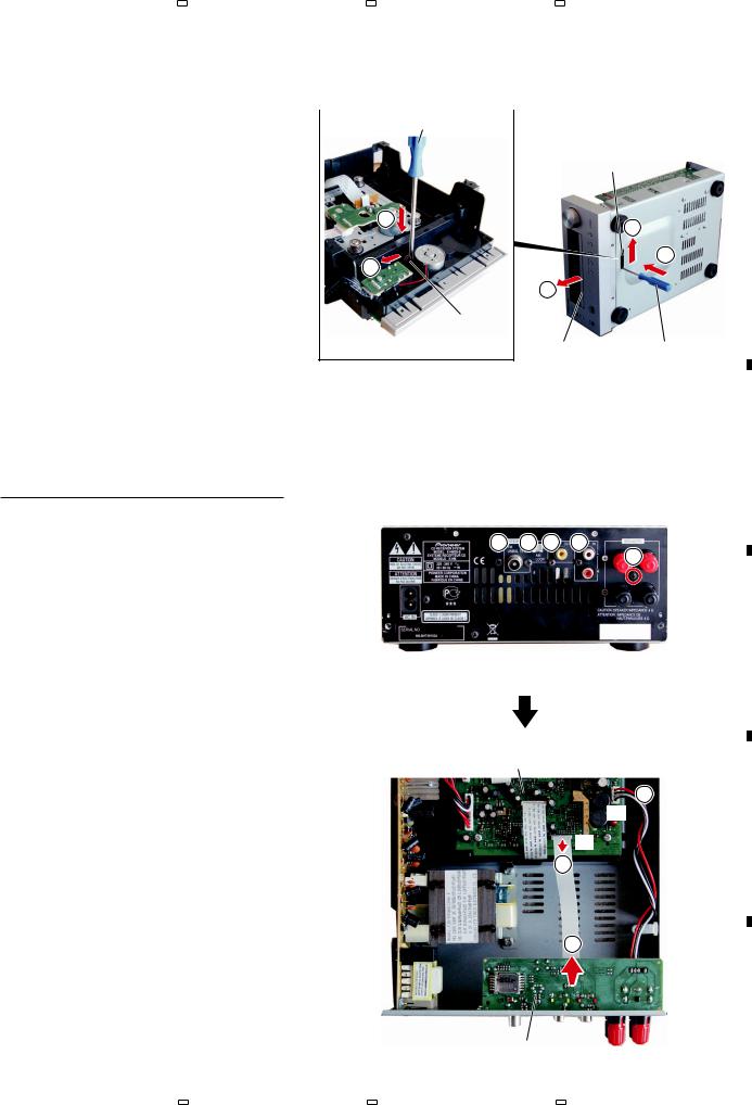
[2] iPOD PCB Assy (X-HM20 only)
(1)Remove the top cabinet.
(See procedure "[1] Top Cabinet".)
(1)Disconnect the one flexible cable and one connectors. (J802, J803)
(2)Remove the two screws.
(3)Remove the iPOD PCB Assy.
1 |
1 |
1 |
1 |
2 2
2 |
2 |
|
• Rear view |
3
Top cabinet
Top cabinet |
iPOD PCB Assy |
3
2
 2
2
J803 J802
1 1
• Bottom view
X-HM20-K |
13 |
A
B
C
D
E
F
|
5 |
|
6 |
|
7 |
|
8 |
|
|
|
|
|
|

|
1 |
|
2 |
|
3 |
|
4 |
|
|
|
|
|
|
A [3] Front Panel Section
(1)Remove the top cabinet.
(See procedure "[1] Top Cabinet".)
(1)Remove the two screws.
(2)Remove the two screws.
(3)Unhook the two hooks.
3 |
3 |
1 |
1 |
2 |
2 |
• Bottom view
B
(4) |
Disconnect the one flexible cable and three |
|
MAIN PCB Assy |
|
|
||||
|
|
connectors. (J3, J5, J12, J14) |
|
|
|
|
|
|
|
|
(5) |
Release the jumper wires from hook. |
|
|
|
|
|
|
|
|
(6) |
Remove the one screw. |
4 |
J3 |
|
|
|
|
|
|
|
|
|||||||
|
|
|
|
|
|
|
|
|
|
|
|
|
|
|
|
|
|
|
|
|
|
6 |
|
|
|
|
|
J14 |
|
|
|
4 |
J12 |
|
|
||||
|
|
|
J5 |
||||||
|
|
|
|
|
|
||||
C |
5 |
|
|
|
|
|
|||
|
|
|
|
|
|
|
|||
|
|
|
|
|
|
|
|
|
|
|
|
|
|
|
|
|
|
|
|
 4
4
 4
4
(7) |
Remove the volume knob. |
|
|
(8) Remove the nut and washers. |
|
D (9) |
Remove the front panel section. |
|
|
|
|
|
|
|
(10) Remove the two screws.
E(11) Remove the 12 screws.
(12)Remove the DISPLAY, KEY-SWITCH, HEADPHONE and USB PCB Assemblies.
F
Volume knob
7 8
9
Front panel section
HEADPHONE PCB Assy |
KEY-SWITCH PCB Assy |
|||||
|
|
10 USB PCB Assy |
||||
11 |
|
11 |
11 |
|
||
|
|
|
10 |
|
|
|
|
|
|
|
|
11 |
|
|
|
|
|
|
|
|
11 |
12 |
11 |
12 |
11 |
12 |
11 |
|
|
11 |
|
|
|
11 |
|
11 |
|
12 |
|
11 |
|
|
|
|
|
|||
DISPLAY PCB Assy
14 |
X-HM20-K |
|
1 |
|
2 |
|
3 |
|
4 |
|
|
|
|
|
|
|
5 |
|
6 |
|
7 |
|
8 |
|
|
|
|
|
|
How to open the tary when the power cannot be on |
|
A |
||||
(1) |
Insert the thin minus screwdriver to the slit. |
|
|
|
|
|
|
Thin minus screwdriver |
|||||
(2) |
Slide the lever in the arrow direction. |
|||||
|
|
|
||||
(3) |
Pull out the tray by hand. |
|
|
|
||
|
|
|
|
Slit |
||
|
|
|
|
|
|
|
|
|
|
|
|
|
|
1 |
2 |
|
|
2 |
1 |
B |
|
|
3 |
|
Lever |
• Bottom view |
Tray Thin minus screwdriver |
[4] RADIO PCB Assy
C
(1)Remove the top cabinet.
(See procedure "[1] Top Cabinet".)
(1)Remove the five screws.
(2)Disconnect the one flexible cable and one connectors. (J1, J6)
(3)Remove the RADIO PCB Assy.
1 1 1 1 

 1
1
D
• Rear view
MAIN PCB Assy
 2
2
J6
E
J1
2
3
F
RADIO PCB Assy
X-HM20-K |
15 |
|
5 |
|
6 |
|
7 |
|
8 |
|
|
|
|
|
|
|
1 |
|
2 |
|
3 |
|
4 |
|
|
|
|
|
|
A[5] POWER PCB Assy
(1)Remove the top cabinet.
(See procedure "[1] Top Cabinet".)
(1)Remove the two screws.
B
(2) Remove the one screw.
C
 1
1
 1
1
• Bottom view
2
• Rear view
D
(3) Remove the three screws.
POWER PCB Assy
3
3 3
E
(4)Remove the two screws.
(5)Disconnect the two connectors. (J9, J11)
(6)Remove the POWER PCB Assy.
F
16
MAIN PCB Assy
4 4
J9 J11

 6 5 5
6 5 5
POWER PCB Assy
X-HM20-K
|
1 |
|
2 |
|
3 |
|
4 |
|
|
|
|
|
|

|
5 |
|
6 |
|
7 |
|
8 |
|
|
|
|
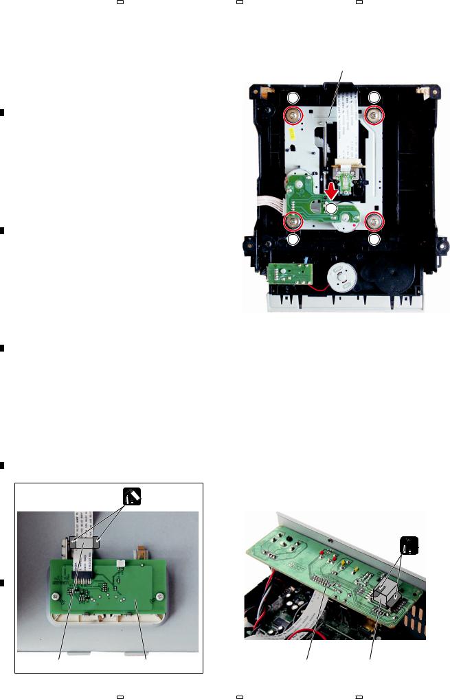
[6] MAIN PCB Assy, LOADER Assy, CD MECHA Unit
(1)Remove the top cabinet.
(See procedure "[1] Top Cabinet".)
(2)Remove the front panel section.
(See procedure "[3] Front Panel Section".)
(1)Disconnect the two flexible cables and five connectors. (J1, J6, J9, J10, J11, J13, J19)
(2)Remove the four screws.
(3)Remove the MAIN PCB Assy.
MAIN PCB Assy
|
2 |
1 |
|
2 |
|
|
|
|
|
||
|
|
J1 |
1 |
J11 |
1 |
|
|
|
|
||
1 |
J6 |
|
J19 |
|
|
|
|
|
|
J9 |
1 |
|
|
|
|
J13 |
1 |
|
|
|
3 |
J10 |
1 |
2 |
2 |
(4)Remove the three screws.
(5)Remove the LOADER Assy.
4 |
4 |
5
4
LOADER Assy
A
B
C
D
E
F
X-HM20-K |
17 |
|
5 |
|
6 |
|
7 |
|
8 |
|
|
|
|
|
|
|
1 |
|
2 |
|
3 |
|
4 |
|
|
|
|
|
|
A(6) Remove the four screws.
(7) Remove the CD MECHA Unit.
Note:
Removal of the disc tray cover is not required during disassembly/reassembly of the front panel section, because this cover does not interfere with the front panel.
B
C
D
CD MECHA Unit
6 |
6 |
7
6 |
6 |
 • Bottom view Disc tray cover
 The Application Position of Adhesive
X-HM20 ONLY
Adhesive (No.1600B)
GYL1007
E

 Adhesive (No.1600B)
GYL1007
F
Ferrite core |
iPOD PCB Assy |
RADIO PCB Assy |
Gasket |
||
18 |
|
|
|
|
|
|
|
X-HM20-K |
|
|
|
|
|
|
|
|
|
|
1 |
|
2 |
|
3 |
|
4 |
|
|
|
|
|
|
 Loading...