


VSXD-812
Table of contents
 Loading...
ORDER NO.
PIONEER CORPORATION 4-1, Meguro 1-chome, Meguro-ku, Tokyo 153-8654, Japan
PIONEER ELECTRONICS (USA) INC. P.O. Box 1760, Long Beach, CA 90801-1760, U.S.A.
PIONEER EUROPE NV Haven 1087, Keetberglaan 1, 9120 Melsele, Belgium
PIONEER ELECTRONICS ASIACENTRE PTE. LTD. 253 Alexandra Road, #04-01, Singapore 159936
PIONEER CORPORATION 2003
DOWN UP
ENTER
MASTERVOLUME
MULTIJOG
PHONES
STANDBY
STANDBY/ON
PULL OPEN
DVD/LD TV/SAT VCR/DVR VIDEO
CD
CD-R/
TAPE/MD
TUNER
AUX
VSX-D912-S
RRV2745
AUDIO/VIDEO MULTI-CHANNEL RECEIVER
VSX-D912-S
VSX-D812-K
VSX-D812-S
THIS MANUAL IS APPLICABLE TO THE FOLLOWING MODEL(S) AND TYPE(S).
Model Type Power Requirement Remarks
VSX-D912-S MYXJIEW AC220-230V
VSX-D812-K MYXJIEW AC220-230V
VSX-D812-S MYXJIEW AC220-230V
VSX-D812-S MYXJIFG AC220-230V
For details, refer to "Important symbols for good services".
T-ZZK APR. 2003 printed in Japan
VSX-D912-S
2
1234
1234
C
D
F
A
B
E
SAFETY INFORMATION
This service manual is intended for qualified service technicians; it is not meant for the casual
do-it-yourselfer. Qualified technicians have the necessary test equipment and tools, and have been
trained to properly and safely repair complex products such as those covered by this manual.
Improperly performed repairs can adversely affect the safety and reliability of the product and may
void the warranty. If you are not qualified to perform the repair of this product properly and safely, you
should not risk trying to do so and refer the repair to a qualified service technician.
WARNING
This product contains lead in solder and certain electrical parts contain chemicals which are known to the state of California to
cause cancer, birth defects or other reproductive harm.
Health & Safety Code Section 25249.6 – Proposition 65
NOTICE
(FOR CANADIAN MODEL ONLY)
Fuse symbols (fast operating fuse) and/or (slow operating fuse) on PCB indicate that replacement
parts must be of identical designation.
REMARQUE
(POUR MODÈLE CANADIEN SEULEMENT)
Les symboles de fusible (fusible de type rapide) et/ou (fusible de type lent) sur CCI indiquent que
les pièces de remplacement doivent avoir la même désignation.
ANY MEASUREMENTS NOT WITHIN THE
LIMITS OUTLINED ABOVE ARE INDICATIVE
OF A POTENTIAL SHOCK HAZARD AND
MUST BE CORRECTED BEFORE RETURN-
ING THE APPLIANCE TO THE CUSTOMER.
2. PRODUCT SAFETY NOTICE
Many electrical and mechanical parts in the appliance
have special safety related characteristics. These are
often not evident from visual inspection nor the
protection afforded by them necessarily can be obtained
by using replacement components rated for voltage,
wattage, etc. Replacement parts which have these
special safety characteristics are identified in this
Service Manual.
Electrical components having such features are
identified by marking with a
on the schematics and
on the parts list in this Service Manual.
The use of a substitute replacement component which
does not have the same safety characteristics as the
PIONEER recommended replacement one, shown in the
parts list in this Service Manual, may create shock, fire,
or other hazards.
Product Safety is continuously under review and new
instructions are issued from time to time. For the latest
information, always consult the current PIONEER
Service Manual. A subscription to, or additional copies
of, PIONEER Service Manual may be obtained at a
nominal charge from PIONEER.
(FOR USA MODEL ONLY)
1. SAFETY PRECAUTIONS
The following check should be performed for the
continued protection of the customer and service
technician.
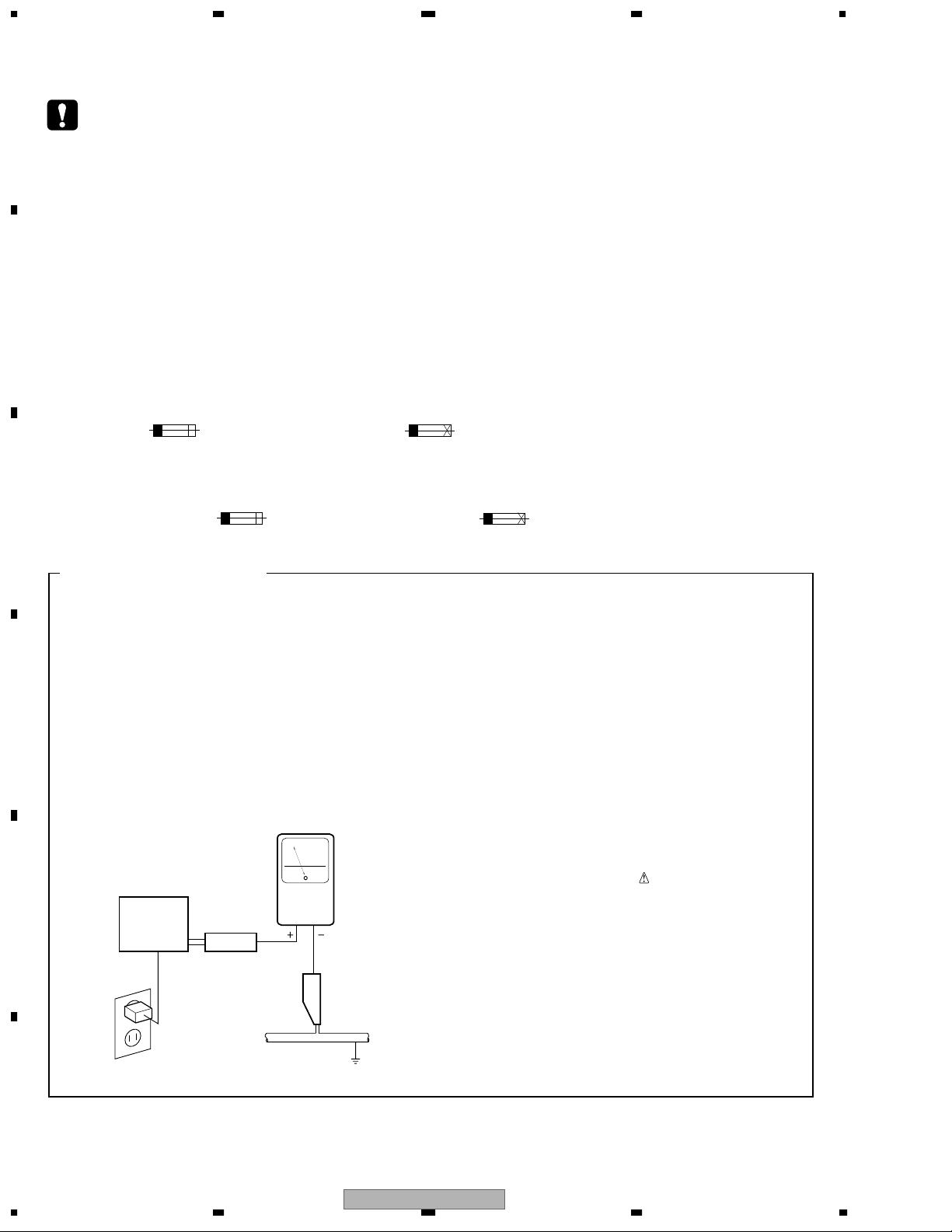
LEAKAGE CURRENT CHECK
Measure leakage current to a known earth ground
(water pipe, conduit, etc.) by connecting a leakage
current tester such as Simpson Model 229-2 or
equivalent between the earth ground and all exposed
metal parts of the appliance (input/output terminals,
screwheads, metal overlays, control shaft, etc.). Plug
the AC line cord of the appliance directly into a 120V
AC 60 Hz outlet and turn the AC power switch on. Any
current measured must not exceed 0.5 mA.
Device
under
test
Leakage
current
tester
Earth
ground
Reading should
not be above
0.5 mA
Also test with
plug reversed
(Using AC adapter
plug as required)
Test all
exposed metal
surfaces
AC Leakage Test
VSX-D912-S
3
5678
56
7
8
C
D
F
A
B
E
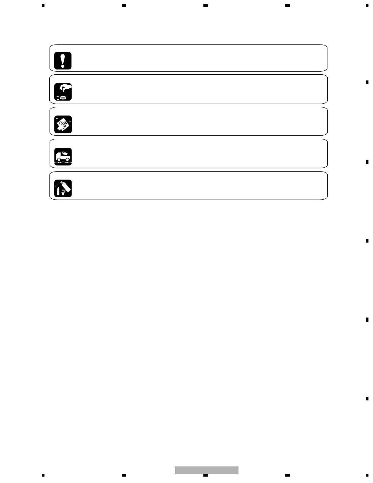
[ Important symbols for good services ]
In this manual, the symbols shown-below indicate that adjustments, settings or cleaning should be made securely.
When you find the procedures bearing any of the symbols, be sure to fulfill them:
2. Adjustments
To keep the original performances of the product, optimum adjustments or specification confirmation is indispensable.
In accordance with the procedures or instructions described in this manual, adjustments should be performed.
3. Cleaning
For optical pickups, tape-deck heads, lenses and mirrors used in projection monitors, and other parts requiring cleaning,
proper cleaning should be performed to restore their performances.
5. Lubricants, glues, and replacement parts
Appropriately applying grease or glue can maintain the product performances. But improper lubrication or applying
glue may lead to failures or troubles in the product. By following the instructions in this manual, be sure to apply the
prescribed grease or glue to proper portions by the appropriate amount.For replacement parts or tools, the prescribed
ones should be used.
4. Shipping mode and shipping screws
To protect the product from damages or failures that may be caused during transit, the shipping mode should be set or
the shipping screws should be installed before shipping out in accordance with this manual, if necessary.
1. Product safety
You should conform to the regulations governing the product (safety, radio and noise, and other regulations), and
should keep the safety during servicing by following the safety instructions described in this manual.

VSX-D912-S
4
1234
1234
C
D
F
A
B
E
CONTENTS
SAFETY INFORMATION ..................................................................................................................................... 2
1. SPECIFICATIONS ............................................................................................................................................5
2. EXPLODED VIEWS AND PARTS LIST ............................................................................................................ 7
2.1 PACKING ................................................................................................................................................... 7
2.2 EXTERIOR SECTION................................................................................................................................ 8
2.3 FRONT PANEL SECTION ....................................................................................................................... 10
3. BLOCK DIAGRAM AND SCHEMATIC DIAGRAM..........................................................................................12
3.1 BLOCK DIAGRAM ................................................................................................................................... 12
3.2 OVERALL WIRING CONNECTION DIAGRAM........................................................................................ 14
3.3 MAIN ASSY (1/3) ..................................................................................................................................... 16
3.4 MAIN ASSY (2/3) ..................................................................................................................................... 18
3.5 MAIN ASSY (3/3) ..................................................................................................................................... 20
3.6 DSP ASSY (1/2)....................................................................................................................................... 22
3.7 DSP ASSY (2/2)....................................................................................................................................... 24
3.8 AMP & PRIMARY (1/2), TRANS2 and TRANS3 ASSYS ......................................................................... 26
3.9 AMP & PRIMARY (2/2), REG. , AMP INPUT and TRANS1 ASSYS ........................................................ 28
3.10 VIDEO, 6CH IN, BOARD TO BOARD and S. VIDEO ASSYS ................................................................ 30
3.11 FRONT, R. ENCODER and POWER SW ASSYS ................................................................................. 32
3.12 TRANS4, F.VIDEO, H.P., PRE., D.IN and F.OPT&MIC ASSYS.............................................................. 34
3.13 FM/AM TUNER MODULE...................................................................................................................... 36
4. PCB CONNECTION DIAGRAM ..................................................................................................................... 38
4.1 REGULATOR ASSY................................................................................................................................. 38
4.2 TRANS2, TRANS3, TRANS1 and TRANS4 ASSYS................................................................................ 39
4.3 MAIN ASSY ............................................................................................................................................. 40
4.4 DSP ASSY ............................................................................................................................................... 44
4.5 AMP & PRIMARY and AMP INPUT ASSYS............................................................................................ 46
4.6 FRONT, R. ENCODER, POWER SW and H. P. ASSYS .......................................................................... 48
4.7 BOARD TO BOARD, DIGITAL IN, VIDEO and 6CH IN ASSYS ............................................................... 52
4.8 S.VIDEO, F.VIDEO, F.OPT&MIC and PRE-OUT ASSYS......................................................................... 54
4.9 FM/AM TUNER MODULE........................................................................................................................ 56
5. PCB PARTS LIST ........................................................................................................................................... 57
6. ADJUSTMENT ............................................................................................................................................... 64
6.1 TUNER SECTION ....................................................................................................................................64
7. GENERAL INFORMATION ............................................................................................................................. 65
7.1 DIAGNOSIS ............................................................................................................................................. 65
7.1.1 DISASSEMBLY AND DIAGNOSIS........................................................................................................ 65
7.1.2 PCB LOCATION.................................................................................................................................... 66
7.2 PARTS...................................................................................................................................................... 67
7.2.1 IC .......................................................................................................................................................... 67
7.2.2 DISPLAY ............................................................................................................................................... 81
7.3 EXPLANATION ........................................................................................................................................ 83
7.3.1 POWER ON AND OFF INITIAL TIMING CHART.................................................................................. 83
7.3.2 IC DATA TRANSMISSION TIMING CHART.......................................................................................... 85
7.3.3 DETECTION CIRCUIT.......................................................................................................................... 86
7.3.4 AMPLIFIER SYSTEM PROTECTION OPERATION SPECIFICATION................................................. 87
7.4 CLEANING............................................................................................................................................... 87
8. PANEL FACILITIES ........................................................................................................................................ 88

VSX-D912-S
5
5678
56
7
8
C
D
F
A
B
E
1. SPECIFICATIONS
+0
–3
+0
–3
• Amplifier section
Continuous power output (stereo)
These specifications are applicable when the power supply
is 230 V.
Front.........................................................100 W per channel
(DIN 1kHz, THD 1 %, 8 Ω)
Continuous power output (surround)
These specifications are applicable when the power supply
is 230 V.
Front.........................................................100 W per channel
(1kHz, 1.0 %, 8 Ω)
Center......................................................100 W per channel
(1kHz, 1.0 %, 8 Ω)
Surround..................................................100 W per channel
(1kHz, 1.0 %, 8 Ω)
Surround Back.........................................100 W per channel
(1kHz, 1.0 %, 8 Ω)
Input (Sensitivity/Impedance)
CD, VCR/DVR, CD-R/TAPE/MD,
DVD/LD, TV/SAT.............................................200 mV/47 kΩ
Frequency response
CD, VCR/DVR, CD-R/TAPE/MD,DVD/LD,
TV/SAT...........................................5 Hz to 100,000 Hz dB
Output (Level/Impedance)
VCR/DVR REC, CD-R/TAPE/MD REC............200mV/2.2kΩ
Tone control
Bass..............................................................± 6 dB (100 Hz)
Treble............................................................± 6 dB (10 kHz)
Loudness............................± 6.5 dB/+3 dB (100 Hz/10 kHz)
(at volume level -50 dB)
Signal-to-Noise Ratio
[DIN (Continuous rated power output/50 mW)]
CD, VCR/DVR, CD-R/TAPE/MD, DVD/LD, TV/SAT.....96 dB
• Video Section
Input (Sensitivity/Impedance)
VCR/DVR, DVD/LD, TV/SAT..............................1 Vp-p/75 Ω
Output (Level/Impedance)
VCR/DVR, MONITOR OUT................................1 Vp-p/75 Ω
Frequency Response
VCR/DVR, DVD/LD,
TV/SAT ⇒ MONITOR............................5 Hz to 7 MHz dB
Signal-to-Noise Ratio....................................................55 dB
• FM Tuner Section
Frequency Range................................87.5 MHz to 108 MHz
Usable Sensitivity....................................Mono:13.2 dBf, IHF
(1.3 µV/ 75 Ω)
50 dB Quieting Sensitivity...............................Mono: 20.2 dB
Stereo: 38.6 dBf
Signal-to-Noise RatioStereo.............Mono: 73 dB (at 85 dBf)
Stereo: 70 dB (at 85 dBf)
Distortion..............................................Stereo: 0.5 % (1 kHz)
Alternate Channel Selectivity........................................60 dB
(400 kHz)
Stereo Separation............................................40 dB (1 kHz)
Frequency response.....................................30 Hz to 15 kHz
(±1 dB)
Antenna Input (DIN)....................................75 Ω unbalanced
• AM Tuner Section
Frequency range..................................531 kHz to 1,602 kHz
Selectivity (IHF, Loop antenna)..............................350 µV/m
Selectivity......................................................................25 dB
Signal-to-Noise Ratio....................................................50 dB
Antenna............................................................Loop antenna
• Miscellaneous
Power Requirements........................AC 220-230 V, 50/60Hz
Power Consumption.....................................................280 W
In standby..................................................................0.5 W
Dimensions.........................420 (W) x 158 (H) x 401 (D) mm
Weight (without package)...........................................10.0 kg

VSX-D912-S
6
1234
1234
C
D
F
A
B
E
Accessories
Remote control unit
(XXD3054)
Microphone
(APM7004)
Microphone Stand
(AEB7269)
VSX-D912 Only
• Furnished Parts
AM loop antenna..................................................................1
FM wire antenna...................................................................1
Dry cell batteries (AA size IEC R6)......................................2
Remote control.....................................................................1
Microphone (VSX-D912 only)...............................................1
Microphone stand (VSX-D912 only).....................................1
These operating instructions................................................1
• Specifications and the design are subject to possible
modifications without notice, due to improvements.
Cleaning the unit
• Use a polishing cloth or dry cloth to wipe off dust and dirt.
• When the surface is dirty, wipe with a soft cloth dipped in
some neutral cleanser diluted five or six times with water,
and wrung out well, and then wipe again with a dry cloth.
Do not use furniture wax or cleansers.
• Never use thinners, benzine, insecticide sprays or other
chemicals on or near this unit, since these will corrode the
surface.
Note
Manufactured under license from Dolby
Laboratories. "Dolby", "Pro Logic",
"Surround EX", and the double-D symbol
are trademarks of Dolby Laboratories.
"DTS" ,"DTS-ES Extended Surround" and
"Neo:6" are trademarks of Digital Theater
Systems, Inc.
SOURCE
MULTI CONTROL
RECEIVER
INPUT SELECT
STEREO/
DIRECT
MIDNIGHT/
LOUDNESS
ADVANCED
SURROUND
LEVEL
EFFECT
RECEIVER CONTROL
CH
SELECT
STANDARD
BANDRETURN
RF ATT
A
EDCB
DISC
DISPLAY CLASS MPX D.ACCESS
TV CONTROL
MUTE
TOP MENU MENU
SETUP
AUDIO
INPUT ATT
T.EDIT
GUIDE
SUBTITLE
MCACC
SETUP
SLEEP
CHANNEL VOLUME
INPU
T
SEL
ECT
+
10
TEST
TONE
FL
DIMMER
RECEIVER
ST
TUNE
MASTER
VOLUME
ST
TUNE
CHANNEL
DVD/LD
ENTER
ENTER
TV/SAT
CD
VCR/DVR TV CONT
TUNER
CD-R/TAPE
RECEIVER
123
456
7890
AA size IEC R6
Dry cell batteries (x2)
AM loop antenna
(ATB7009)
FM wire antenna
(ADH7030)
VSX-D912-S
7
5678
56
7
8
C
D
F
A
B
E
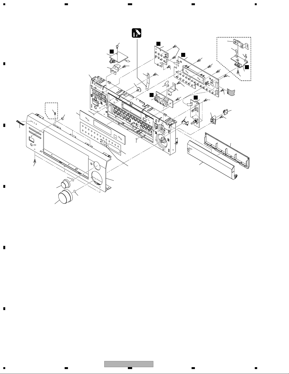
2. EXPLODED VIEWS AND PARTS LIST
2.1 PACKING
PACKING parts List
(2) CONTRAST TABLE
VSX-D912-S/MYXJIEW, VSX-D812-K/MYXJIEW, VSX-D812-S/MYXJIEW and MYXJIFG are constructed the same
except for the following:
Parts marked by "NSP" are generally unavailable because they are not in our Master Spare Parts List.
The mark found on some component parts indicates the importance of the safety factor of the part.
Therefore, when replacing, be sure to use parts of identical designation.
Screws adjacent to mark on product are used for disassembly.
For the applying amount of lubricants or glue, follow the instructions in this manual.
(In the case of no amount instructions, apply as you think it appropriate.)
NOTES:
1
3
2
4
15
8
10
11
6
9
12
17
5
16
7
14
13
VSX-D912-S ONLY
MYXJIEW
TYPE ONLY
Mark
No. Description Part No.
1 FM wire antenna ADH7030
NSP 2 Warranty Card ARY7065
3 AM loop antenna ATB7009
NSP 4 Dry cell batteries (AA/R6) VEM1031
5 Operating instructions See Contrast table(2)
(English/Italian)
6 Remote Control Unit XXD3054
7 Battery Cover AZA7424
NSP 8 Literature Bag AHG1180
9 Packing Sheet AHG7069
10 Left Pad R6 XHA3134
11 Right Pad R6 XHA3135
12 Packing Case See Contrast table(2)
13 MIC Stand 45 See Contrast table(2)
14 Microphone Assy See Contrast table(2)
NSP 15 Accessory Board R6 XHB3008
16 Operating instructions See Contrast table(2)
(Dutch/Spanish)
17 Operating instructions XRC3082
(French/German)
Mark
No. Description Part No.
Mark NO Symbol and Description
VSX-D912-S/
MYXJIEW
VSX-D812-K/
MYXJIEW
VSX-D812-S/
MYXJIEW
VSX-D812-S/
MYXJIFG
5 Operating Instructions (English/Italian) XRE3070 XRE3070 XRE3070 Not used
12 Packing Case XHD3334 XHD3332 XHD3333 XHD3333
13 MIC Stand 45 AEB7269 Not used Not used Not used
14 Microphone Assy APM7004 Not used Not used Not used
16 Operating Instructions (Dutch/Spanish) XRC3081 XRC3081 XRC3081 Not used

VSX-D912-S
8
1234
1234
C
D
F
A
B
E
2.2 EXTERIOR SECTION
50
F
P
O
R
Q
S
C
L
I
L
S
Q
P
O
R
J
J
K
K
I
B
F
A
B
B
B
C
A
E
D
E
M
M
Q
H
H
D
NON-CONTACT
SIDE
CONTACT
SIDE
W
L
K
I
A
T
B
F
D
H
E
P
G
C
S
J
45
18
52
53
23
24
52
8
5
13
4
38
46
54
54
36
34
35
20
39
40
40
51
6
9
1
12
11
10
17
21
22
44
14
2
15
33
48
30
31
32
37
29
28
27
58
49
43
42(2/2)
41
42(1/2)
Refer to
"2.3 FRONT PANEL SECTION".
26
7
3
EXCEPT
VSX-D812-K
56
56
55
55
55
57
57
55
55
55
55
55
55
55
55
55
55
62
55
55
55
55
55
55
55
55
55
55
55
55
55
55
55
55
55
55
47
55
55
55
55
55
55
55
60
55
55
55
61
VSX-D912-S
9
5678
56
7
8
C
D
F
A
B
E
EXTERIOR SECTION parts List
(2) CONTRAST TABLE
VSX-D912-S/MYXJIEW, VSX-D812-K/MYXJIEW, VSX-D812-S/MYXJIEW and MYXJIFG are constructed the
same except for the following:
Mark
No. Description Part No.
1 MAIN Assy See Contrast table(2)
2 DSP Assy AWX1082
3 AMP&PRIMARY Assy XWZ3670
4 TRANS2 Assy XWZ3684
5 TRANS3 Assy XWZ3687
6 REGULATOR Assy XWZ3676
7 AMP INPUT Assy XWZ3679
8 TRANS1 Assy XWZ3681
9 VIDEO Assy XWZ3647
10 6CH IN Assy XWZ3650
11 BOARD TO BOARD Assy XWZ3665
12 S. VIDEO Assy XWZ3660
13 TRANS4 Assy XWZ3662
14 PRE-OUT Assy XWZ3663
15 DIGITAL IN Assy See Contrast table(2)
16 • • • • • •
17 FM/AM TUNER MODULE AXQ7232
>
18 FU1 Fuse (T3.15A) REK1027
19 • • • • • •
>
20 T1 Power Transformer XTS3063
>
21 AC Power Cord VDG1080
22 Cord Stopper CM-22B
23 J36 23P F.F.C/30V XDD3102
24 J46 7P F.F.C/30V XDD3105
25 • • • • • •
26 J22 3P F.F.C/30V XDD3107
27 J33 11P F.F.C/30V XDD3123
28 J48 9P F.F.C/30V XDD3124
29 J34 13P F.F.C/30V XDD3122
30 J43 19P F.F.C/30V XDD3126
31 J31 17P F.F.C/30V XDD3118
32 J35 19P F.F.C/30V XDD3101
33 J37 10P F.F.C/30V XDD3127
NSP 34 Heatsink R6A CORR XNH3026
35 H/S Angle Rear XNG3095
36 H/S Angle Front XNG3094
37 PCB Angle R5 XNG3073
38 PCB Mold AMR2533
NSP 39 Under Base R6 XNA3012
40 Insulator PNW2766
>
41 DC Fan Motor XXM3006
42 Fan Holder R6 XMR3066
43 REG Support R6 XNG3093
44 Rear Panel 812K XNC3196
45 Bonnet See Contrast table(2)
NSP 46 HOLDER Assy XWZ3693
47 FFC Holder R6 XMR3072
48 Shield A R6 XNG3068
49 FFC Cover R6 XMR3060
NSP 50 N Label See Contrast table(2)
NSP 51 Spacer AEB7092
52 Screw BBZ30P200FMC
53 Screw 3x23 ABA7043
54 Screw FBT40P080FZK
55 Screw BBZ30P080FZK
56 Screw See Contrast table(2)
57 Screw See Contrast table(2)
58 Vjack Spacer R6 XEC3038
NSP 59 BINDER Assy XWZ3691
60 Screw BPZ30P120FMC
61 Fuse Card AAX7493
62 Screw BBT30P100FCC
Mark
No. Description Part No.
Mark NO Symbol and Description
VSX-D912-S/
MYXJIEW
VSX-D812-K/
MYXJIEW
VSX-D812-S/
MYXJIEW
VSX-D812-S/
MYXJIFG
1 MAIN Assy XWK3101 XWK3096 XWK3096 XWK3096
15 DIGITAL IN Assy XWZ3659 XWZ3658 XWZ3658 XWZ3658
45 Bonnet D912S XZN3127 Not used XZN3127 XZN3127
45 Bonnet D912K Not used XZN3126 Not used Not used
NSP 50 N Label 912S/MY XAL3173 Not used Not used Not used
NSP 50 N Label 812S/MY Not used Not used XAL3152 XAL3152
56 Screw BPZ30P080FNI BPZ30P080FZK BPZ30P080FNI BPZ30P080FNI
57 Screw FBT40P080FNI FBT40P080FZK FBT40P080FNI FBT40P080FNI
VSX-D912-S
10
1234
1234
C
D
F
A
B
E
2.3 FRONT PANEL SECTION
M
O
R
Q
V
N
27
28
29
6
1
4
2
3
5
17
16
30
14
13
15
25
7
8
9
10
10
12
VSX-D912-S ONLY
VSX-D912-S ONLY
11
14
18
19
26
20
23
24
22
21
VSX-D812-K,
VSX-D812-S
ONLY
34
34
34
31
34
34
34
34
34
34
34
34
34
34
34
31
Lubricating Oil
GYA1001
VSX-D912-S
11
5678
56
7
8
C
D
F
A
B
E
FRONT PANEL SECTION parts List
(2) CONTRAST TABLE
VSX-D912-S/MYXJIEW, VSX-D812-K/MYXJIEW, VSX-D812-S/MYXJIEW and MYXJIFG are constructed the
same except for the following:
Mark
No. Description Part No.
1 FRONT ASSY XWZ3648
2 R. ENCODER Assy XWZ3653
3 POWER SW Assy XWZ3651
4 FRONT VIDEO Assy XWZ3655
5 H.P. Assy XWZ3654
6 FRONT OPTICAL & MIC Assy See Contrast table(2)
7 Pioneer Badge B See Contrast table(2)
8 Select Knob See Contrast table(2)
9 Volume Knob See Contrast table(2)
NSP 10 C Ring DIM 8.1 XBH3016
11 FRT Panel See Contrast table(2)
12 BN Cover See Contrast table(2)
13 D Panel R6 W XAK3348
14 Cushion See Contrast table(2)
15 LED Lens PNW2019
16 Panel Stay See Contrast table(2)
17 Earth Plate R5 HP XNG3066
18 Door Spring R6 XBK3002
19 J29 8P Shield Cable XDX3012
20 B Lens R6 XAK3352
21 Door See Contrast table(2)
22 Door Cover See Contrast table(2)
23 Holder L R6 XMR3059
24 Damper Assy XXA3025
25 Push Rivet See Contrast table(2)
26 Earth Plate FI R6 XNG3091
27 J30 5P Shield Cable See Contrast table(2)
28 J32 5P F.F.C/30V See Contrast table(2)
29 Earth Plate D R6 See Contrast table(2)
30 Screw XBA3010
31 Screw BBZ30P080FZK
32 • • • • •
33 • • • • •
34 Screw PPZ30P100FMC
Mark
No. Description Part No.
Mark NO Symbol and Description
VSX-D912-S/
MYXJIEW
VSX-D812-K/
MYXJIEW
VSX-D812-S/
MYXJIEW
VSX-D812-S/
MYXJIFG
6 FRONT OPTICAL & MIC Assy XWZ3656 Not used Not used Not used
7 Pioneer Badge B VAM1124 XAM3006 VAM1129 VAM1129
8 SEL Plat Knob R6S XAB3037 Not used XAB3037 XAB3037
8 Select Knob R5BH Not used XAB3023 Not used Not used
9 VOL Plat Knob R6S XAB3036 Not used XAB3036 XAB3036
9 Volume Knob R5BH Not used XAB3025 Not used Not used
11 FRT Panel 912S/MY XNB3001 Not used Not used Not used
11 FRT Panel 812K/MY Not used XMB3106 Not used Not used
11 FRT Panel 812S/MY Not used Not used XMB3107 XMB3107
12 BN Cover 912S/MY XAK3353 Not used Not used Not used
12 BN Cover 712K/MY Not used XAK3378 Not used Not used
12 BN Cover 712S/MY Not used Not used XAK3380 XAK3380
14 Cushion R4G XED3002 Not used XED3002 XED3002
14 Cushion R4B Not used XED3001 Not used Not used
16 Panel Stay 912S/MY XMB3108 Not used Not used Not used
16 Panel Stay 812K/MY Not used XMB3098 Not used Not used
16 Panel Stay 812S/MY Not used Not used XMB3104 XMB3104
21 Door R6S XAK3357 Not used XAK3357 XAK3357
21 Door R6K Not used XAK3356 Not used Not used
22 Door Cover R6S XAK3359 Not used XAK3359 XAK3359
22 Door Cover R6K Not used XAK3358 Not used Not used
25 Push Rivet Not used AEC7025 AEC7025 AEC7025
27 J30 5P Shield Cable XDX3019 Not used Not used Not used
28 J32 5P F.F.C/30V XDD3125 Not used Not used Not used
29 Earth Plate D R6 XNG3092 Not used Not used Not used
VSX-D912-S
12
1234
1234
C
D
F
A
B
E
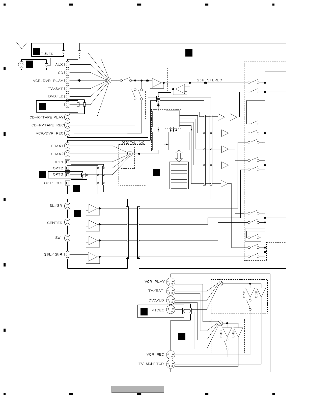
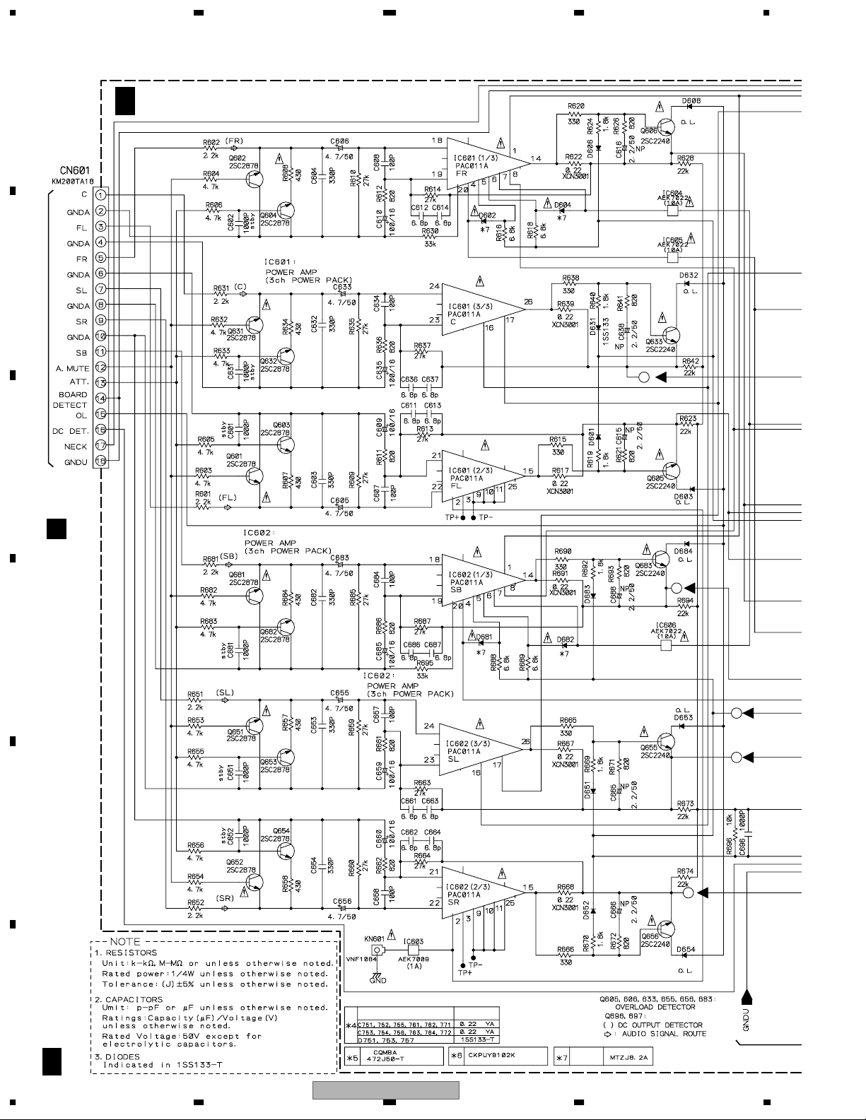
3. BLOCK DIAGRAM AND SCHEMATIC DIAGRAM
3.1 BLOCK DIAGRAM
1
1
3
1
CN103
7
CN108
4
CN201
7
CN307
IC101
BD3841FS
(FUNCTION SEL)
IC303
IC8201
IC302
IC302
NJM2595M
NJM2595M
IC105
IC8401
IC8601
IC8603
(ADC)
(DIR)
(DAC)
(CODEC)
(for DECODE)
IC8501
IS61LV6416
-12T(S-RAM)
IC8602
IS63LV1024
-12T(S-RAM)
PD8116A
(ROM)
MOTOROLA
DSP
A
B
J
T
3
1
7
1
5
9
CN105
7
5
1
4
3
IC304
1
7 3
3
5
3
42
44
46
1
13
8
10
12
19
31
27
24
21
25
23
31
IC103
31
IC104
31
IC104
57
IC107
21
IC106
AK4529VQ
AK4114VQ
uPC4570G2
(LPF)
NJM2100M
31
44
51
47
54
52
45
48
55
19
49
56
IC102
3
1
218
6
24
14 26
L
Q
9
5
7
3
9
5
7
3
11
11
CN901
6
CN354
IC351
IC352
(Y SEL)
(C SEL)
16
Q
W
CN952
VSX-D912 Only
2
V
CN901
3
CN107
1
V
16
8
CN1902
CN8017CN1901
CN951
1
1
Note : When ordering service parts, be sure to refer to "EXPLODED VIEWS and PARTS LIST" or "PCB PARTS LIST".
7
10
1
CN8007
11
7
19
15
13
CN109
7
11
5
3
1
7
10
1
CN109
CN8007
3
17
VSX-D912-S
13
5678
56
7
8
C
D
F
A
B
E
14.1/24.1 14.2/27.3 19.3
IC108
IC109
DB3812F
NJM2595M
BD3813FS
IC110
IC111
IC112
IC112
Q362
Q303
Q603
Q601
Q1552
Q653
Q651
Q632
Q631
uPC4570G2
(PRE AMP)
I
F
CN111
18
CN302
3
30
23
27
21
31
31
IC115
141
31
31
5
7
IC601
24
26
IC602
24
26
IC601
RY751
RY753
RY754
RY752
22
15
R
C
S
G
CN702
6
1551
6
CN106
4
CN601
3
87
11
+12V
-12V
T1
POWER
TRANSFORMER
T51
AC IN
D801–D804
U+5V
D51-D54
RY51
IC51
IC801
T+12V
IC805
CN101
IC802
NECK+B
POWER AMP
IC601, IC602
NECK-B
D702
D701
+BVL
+BVH
-BVH
-BVL
FL AC
FL AC
Q701
Q702
C
C
A
D+5V
D721–D724
IC803
A+5V
IC804
CN101
F
A
CN101
A
CN401
M
IC301
(COMPONENT SEL)
I
9
5
7
1
11
Q
3
CN901
5
CN301
3
Q682
Q681
IC602
18
14
RY752
S
12 11
S
S
VSX-D912-S
14
1234
1234
C
D
F
A
B
E
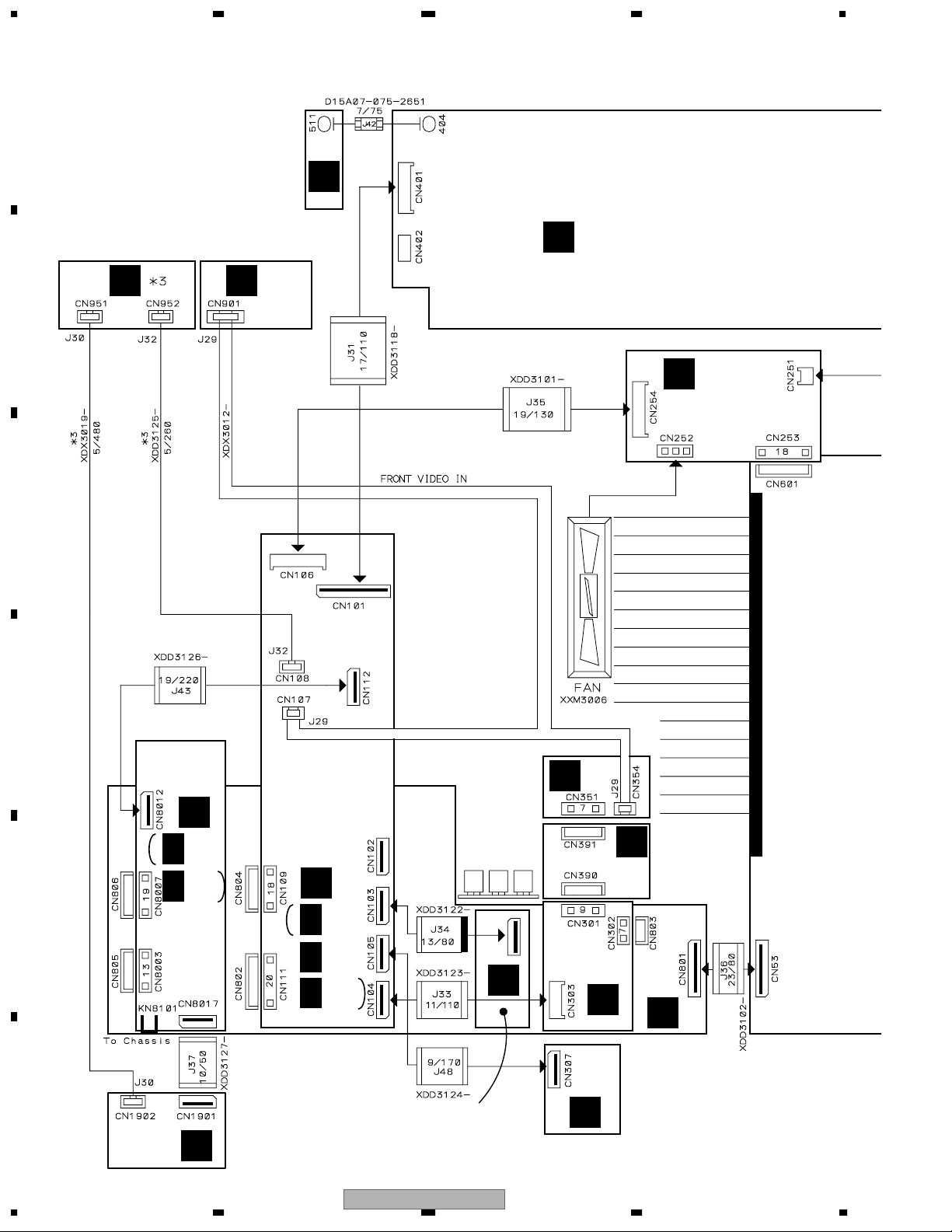
3.2 OVERALL WIRING CONNECTION DIAGRAM
FRONT ASSY
(XWZ3648)
M
DIGITAL IN
ASSY
(VSX-D912
: XWZ3659)
(VSX-D812
: XWZ3658)
T
BOARD TO
BOARD
ASSY
(XWZ3665)
S. VIDEO
ASSY
(XWZ3660)
FRONT
VIDEO ASSY
(XWZ3655)
L
Q
FRONT
OPTICAL
& MIC
ASSY
(XWZ3656)
V
K
R.ENCODER
ASSY
(XWZ3653)
N
MAIN
ASSY
(VSX-D912
: XWK3101)
(VSX-D812
: XWK3096)
A
REGULATOR
ASSY
(XWZ3676)
F
6CH IN ASSY
(XWZ3650)
J
VIDEO
ASSY
(XWZ3647)
FM/AM TUNER
MODULE
(AXQ7232)
I
W
AMP INPUT ASSY
(XWZ3679)
G
A 1/3,
A 2/3,
A 3/3
DSP
ASSY
(AWX1082)
B
B 1/2,
B 2/2

VSX-D912-S
15
5678
56
7
8
C
D
F
A
B
E
PRE-OUT
ASSY
(XWZ3663)
VDG1080
S
VSX-D912 Only
POWER SW ASSY
(XWZ3651)
O
R
H.P. ASSY
(XWZ3654)
TRANS3
ASSY
(XWZ3687)
EP
TRANS2
ASSY
(XWZ3684)
TRANS1
ASSY
(XWZ3681)
D
H
AMP&
PRIMARY
ASSY
(XWZ3670)
C
Y8
Y8
J7J6
J1J2
J4
J5
C 1/2,
C 2/2
TRANS4
ASSY
(XWZ3662)
VSX-D912-S
16
1234
1234
C
D
F
A
B
E
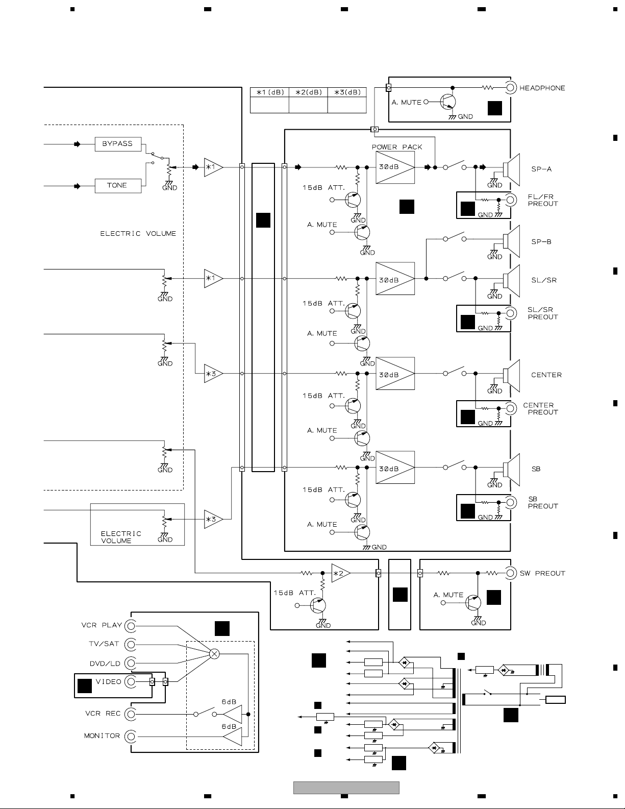
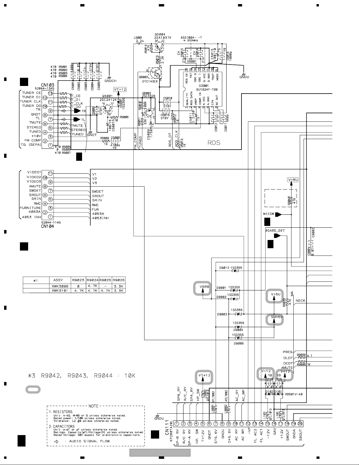
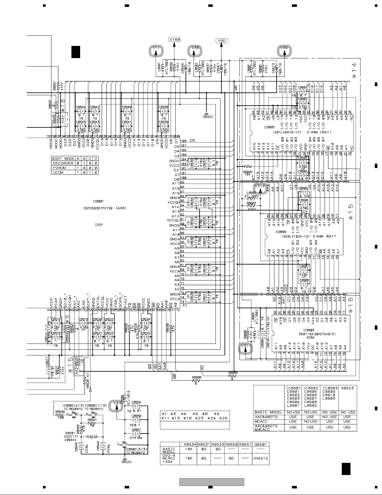
3.3 MAIN ASSY (1/3)
A
A
1/3
VSX-D912 only
VSX-D812,
only
CN901
Q
CN952
V
CN804
F
A 3/3
A 3/3
A 3/3
VSX-D912-S
17
5678
56
7
8
C
D
F
A
B
E
A
1/3
A
1/3
MAIN ASSY
(VSX-D912 : XWK3101)
(VSX-D812 : XWK3096)
: The power supply is shown with the marked box.
A 2/3
A 2/3
A 2/3
A 2/3
A 2/3
A 2/3
A 2/3
A 2/3
A 2/3
A 3/3
VSX-D912-S
18
1234
1234
C
D
F
A
B
E
3.4 MAIN ASSY (2/3)
A
A
2/3
A
2/3
MAIN ASSY
(VSX-D912 : XWK3101)
(VSX-D812 : XWK3096)
A 1/3
A 3/3
A 3/3
CN307
J

VSX-D912-S
19
5678
56
7
8
C
D
F
A
B
E
A
2/3
A 3/3
A 3/3
CN254
G
VSX-D912-S
20
1234
1234
C
D
F
A
B
E
3.5 MAIN ASSY (3/3)
VSX-D812/MY
VSX-D912/MY
A
A
3/3
VSX-D812,
only
A 1/3
A 1/3
A 2/3
: The power supply is shown with the marked box.
CN802
F
CN201
W
CN303
I

VSX-D912-S
21
5678
56
7
8
C
D
F
A
B
E
A
3/3
A
3/3
MAIN ASSY
(VSX-D912 : XWK3101)
(VSX-D812 : XWK3096)
A 2/3
A 2/3
A 1/3
A 1/3
B 2/2
A 2/3
CN8012
CN401
M
VSX-D912-S
22
1234
1234
C
D
F
A
B
E
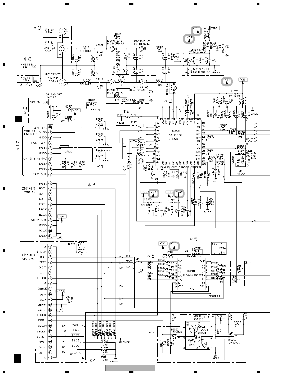
3.6 DSP ASSY (1/2)
A
B
1/2
CN1901
T
NO USE
NO USE
NO USE
NO USE
NO USE

VSX-D912-S
23
5678
56
7
8
C
D
F
A
B
E
B
1/2
B
1/2
DSP ASSY
(AWX1082)
F
F
CN805
CN806
: The power supply is shown with the marked box.
AWX1082 : NO USE
VSX-D912-S
24
1234
1234
C
D
F
A
B
E
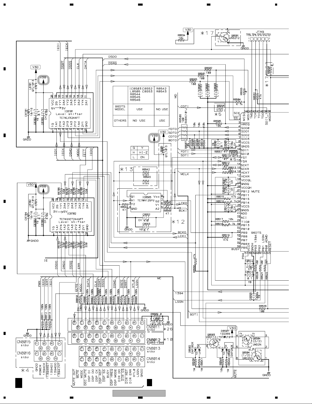
3.7 DSP ASSY (2/2)
A
B
2/2
A 3/3
CN112
VSX-D912-S
25
5678
56
7
8
C
D
F
A
B
E
AWX1082 : NO USE
B
2/2
B
2/2
DSP ASSY
(AWX1082)
VSX-D912-S
26
1234
1234
C
D
F
A
B
E
3.8 AMP & PRIMARY (1/2), TRANS2 and TRANS3 ASSYS
MYXJI
MYXJI
C 1/2
CN253
G
C
1/2
AMP&PRIMARY ASSY
(XWZ3670)
VSX-D912-S
27
5678
56
7
8
C
D
F
A
B
E
MYXJI
MYXJI
MYXJI
MYXJI
D E
TRANS3
ASSY
E
TRANS2
ASSY
(XWZ3684)
D
(XWZ3687)
POWER
TRANSFORMER
1551
R
CN1575
S
CAUTION :
FOR CONTINUED
PROTECTION AGAINST
RISK OF FIRE.
REPLACE ONLY WITH
SAME TYPE NO. 491004
FOR IC851 AND IC852
MFD, BY LITTELFUSE INC.
CAUTION :
FOR CONTINUED
PROTECTION AGAINST
RISK OF FIRE.
REPLACE ONLY WITH
SAME TYPE NO. 491001
FOR IC603 MFD, BY
LITTELFUSE INC.
CAUTION : FOR CONTINUED PROTECTION
AGAINST RISK OF FIRE.
REPLACE ONLY WITH SAME TYPE
NO. 491003 FOR IC853 MFD, BY
LITTELFUSE INC.
CAUTION : FOR CONTINUED PROTECTION
AGAINST RISK OF FIRE.
REPLACE ONLY WITH SAME TYPE
NO. 491010 FOR IC604, IC605, IC606,
AND IC607 MFD, BY LITTELFUSE INC.
C 2/2
C 2/2
C 2/2
• NOTE FOR FUSE REPLACEMENT
FOR CONTINUED PROTECTION AGAINST RISK OF FIRE.
REPLACE WITH SAME TYPE AND RATINGS ONLY.
CAUTION -
CAUTION : FOR CONTINUED PROTECTION
AGAINST RISK OF FIRE.
REPLACE ONLY WITH SAME TYPE
NO. ICP-N10 FOR IC701 AND IC702
MFD, BY ROHM CO., LTD.
C
1/2
VSX-D912-S
28
1234
1234
C
D
F
A
B
E
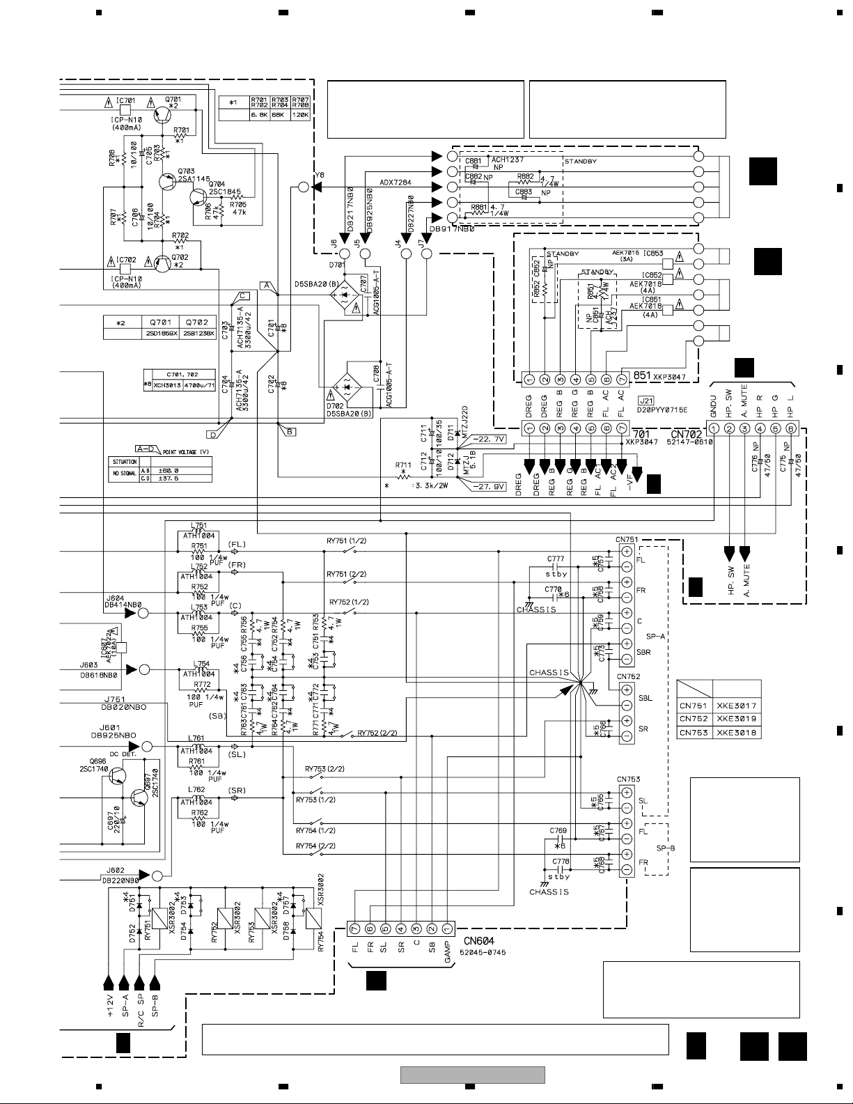
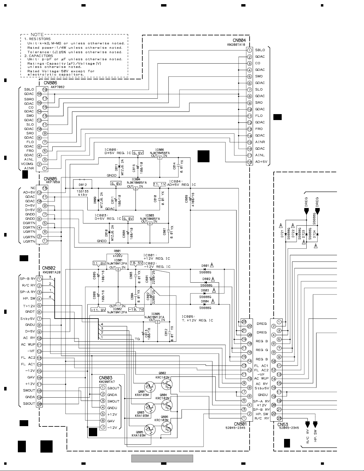
3.9 AMP & PRIMARY (2/2), REG. , AMP INPUT and TRANS1 ASSYS
F
CN111
C 1/2
A 3/3
A 1/3
B 1/2
B 1/2
CN8003
CN302
I
REGULATOR
ASSY
(XWZ3676)
F
C
2/2
CN109
CN8007
Loading...