


HTS3355- 55

1 - 1
HTS3355/
55
©
Copyright 2007 Philips Consumer Electronics B.V. Eindhoven, The Netherlands
All rights reserved. No part of this publication may be reproduced, stored in a retrieval system or
transmitted, in any form or by any means, electronic, mechanical, photocopying, or otherwise
without the prior permission of Philips.
Published by KC-ET0701 Service Audio Printed in The Netherlands Subject to modification
HC
!
DVD Micro Theatre
Version 1.0
TABLE OF CONTENTS
Page
Location of PC Boards ................................................1-2
Versions Variation & Package .................................... 1-2
Specifications .............................................................. 1-3
Service Aids ................................................................1-4
ESD & Safety Instruction ............................................1-5
Lead-free solding Information ....................................1-6
Repair Instructions ......................................................... 2
Disassembly Instructions & Service positions .............. 3
Block & Wiring Diagram ................................................ 4
Control Board ................................................................. 5
Main Board ..................................................................... 6
Power Board .................................................................. 7
DVD loader....................................................................8
Mechanical Exploded View & Parts...............................9
Service Manual
Service
Tfswjdf
Tfswjdf
1 - 2
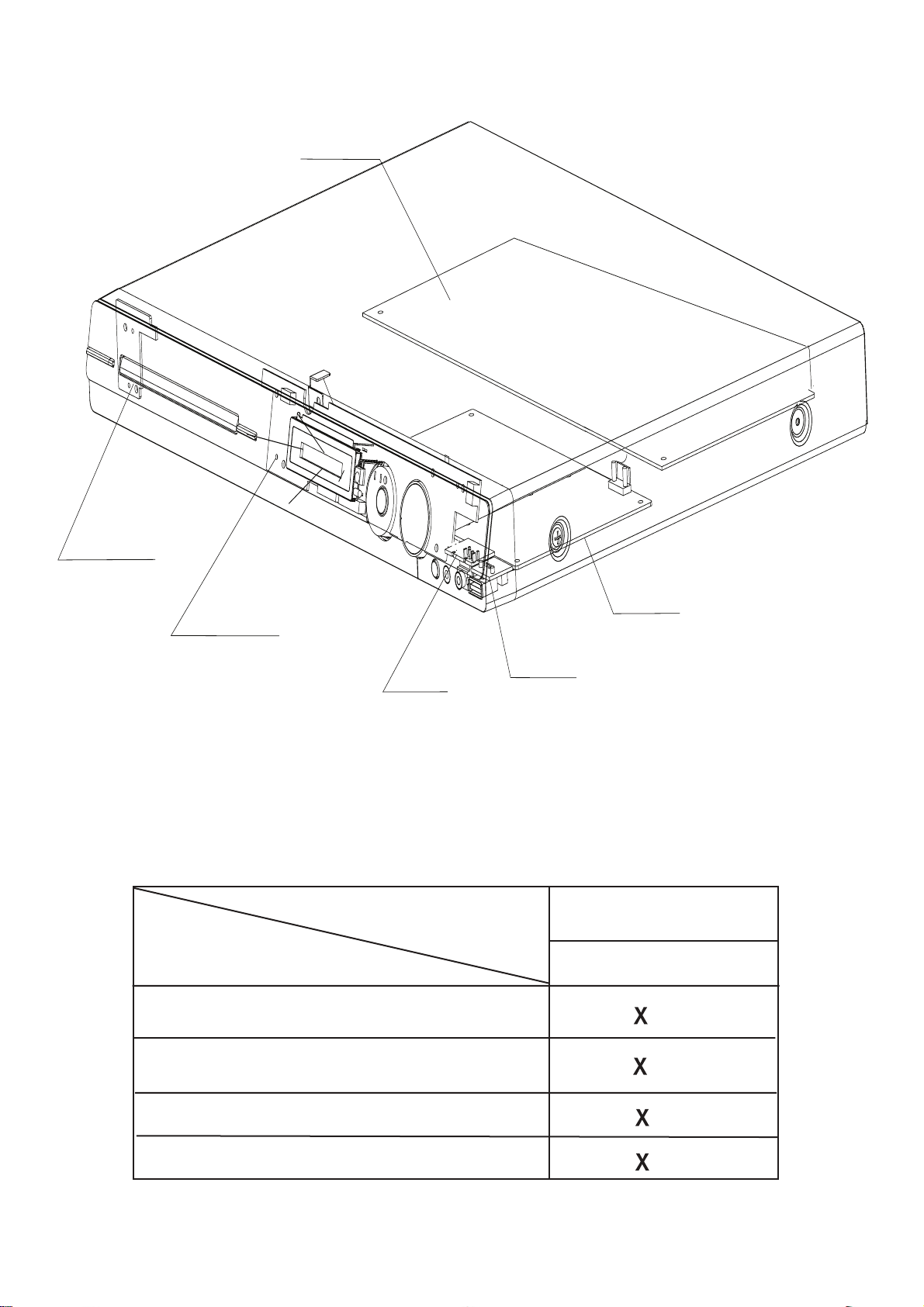
LOCATION OF PCB BOARDS
STANDBY PCB
CONTROL PCB
MP3 PCB
USB PCB
POWER PCB
MAIN PCB
VERSION VARIATION:
Type/Versions
Features & Board in used
HTS3355
/55
Main (Output Power-600W)
Composite Video Out
Power Voltage (120/230V)
AC Cord (Fix)

1 - 3
Speci cations
AMPLIFIER
Total output power . . . . . . . . . . . . . . . . . . . . . . . . . . . . . . . . . . . . . . . . . . . . . . . . . . 600 W RMS
Frequency Response ...... ......... ......... . 150 Hz – 18 kHz / ±3 dB
Signal-to-Noise Ratio . . . . . . . . . . . . . . . . . . . . . . . . . . . . . . . . > 60 dB (A-weighted)
Input Sensitivity
- AUX In . . . . . . . . . . . . . . . . . . . . . . . . . . . . . . . . . . . . . . . . . . . . . . . . . . . . . . . . . . . . . . . . . . . . . . . . . 500 mV
- TV In . . . . . . . . . . . . . . . . . . . . . . . . . . . . . . . . . . . . . . . . . . . . . . . . . . . . . . . . . . . . . . . . . . . . . . . . . . . . 250 mV
- MP3 Line-In . . . . . . . . . . . . . . . . . . . . . . . . . . . . . . . . . . . . . . . . . . . . . . . . . . . . . . . . . . . . . . . . . 500 mV
RADIO
Tuning Range . . . . . . . . . . . . . . . . . . . . . . . . . . . . . . . . . FM 87.5–108 MHz (50kHz)
......................................................... MW 531–1602 kHz (9kHz)
26 dB Quieting Sensitivity . . . . . . . . . . . . . . . . FM 22 dBf, MW 5000µV/m
IF Rejection Ratio . . . . . . . . . . . . . . . . . . . . . . . . . . . . . . . . . . . . FM 60 dB, MW 24 dB
Signal-to-Noise Ratio . . . . . . . . . . . . . . . . . . . . . . . . . . . . . . . FM 50 dB, MW 30 dB
AM Suppression Ratio . . . . . . . . . . . . . . . . . . . . . . . . . . . . . . . . . . . . . . . . . . . . . . . . FM 30 dB
Harmonic Distortion . . . . . . . . . . . . . . . . . . . . . . . . . . . . . . . . . . . . . . . . . . . . . . FM Mono 3%
............................................................................ FM Stereo 3%
.......................................................................................MW 5%
Frequency Response ...... ......... ...... FM 180 Hz–10 kHz / ±6 dB
Stereo Separation . . . . . . . . . . . . . . . . . . . . . . . . . . . . . . . . . . . . . . . . . . FM 26 dB (1 kHz)
Stereo Threshold . . . . . . . . . . . . . . . . . . . . . . . . . . . . . . . . . . . . . . . . . . . . . . . . . . . . . FM 23.5 dB
DISC
Laser Type . . . . . . . . . . . . . . . . . . . . . . . . . . . . . . . . . . . . . . . . . . . . . . . . . . . . . . . . . Semiconductor
Disc Diametre . . . . . . . . . . . . . . . . . . . . . . . . . . . . . . . . . . . . . . . . . . . . . . . . . . . . . . . . . . 12cm / 8cm
Video Decoding . .. . .. .. .. . MPEG-1 / MPEG-2 / DivX 3/4/5/6, Ultra
Video DAC . . . . . . . . . . . . . . . . . . . . . . . . . . . . . . . . . . . . . . . . . . . . . . . . . . . . . . . . . . . . . . . . . . . . . . 12 Bits
Signal System . . . . . . . . . . . . . . . . . . . . . . . . . . . . . . . . . . . . . . . . . . . . . . . . . . . . . . . . . PAL / NTSC
Video Format . . . . . . . . . . . . . . . . . . . . . . . . . . . . . . . . . . . . . . . . . . . . . . . . . . . . . . . . . . . . . . 4:3 / 16:9
Video S/N .... ....... ................... ....... ............ ...... 56 dB (minimum)
Audio DAC . . . . . . . . . . . . . . . . . . . . . . . . . . . . . . . . . . . . . . . . . . . . . . . . . . . . . . . . 24 Bits / 96 kHz
Composite Video Output ...... ......... ......... ......... .... 1.0 Vp-p, 75Ω
S-Video Output . . . . . . . . . . . . . . Y - 1.0 Vp-p, 75Ω C - 0.286 Vp-p, 75Ω
Frequency Response ...... ......... ......... .. 4 Hz–20 kHz (44.1 kHz)
................................................................ 4 Hz–22 kHz (48 kHz)
................................................................ 4 Hz–44 kHz (96 kHz)
PCM . . . . . . . . . . . . . . . . . . . . . . . . . . . . . . . . . . . . . . . . . . . . . . . . . . . . . . . . . . . . . . . . . . . . . . . . . . IEC 60958
Dolby Digital ...... ......... ......... ......... ......... IEC 60958, IEC 61937
DTS .... ....... ............ ....... ....... ............ ...... IEC 60958, IEC 61937
MAIN UNIT
Power Supply Rating . . . . . . . . . . . . . . . . . . . . . . . . . . . . . . . . . . . . . 220~240 V; 50 Hz
Power Consumption . .. .. .. ... .. ... .. .. .. ... .. .. .. ... .. .. .. ... .. ... .. .. .. ... 100 W
Dimensions . . . . . . . . . . . . . . . . . . . . . . . . 340.4 x 48.5 x 435 (mm) (w x h x d)
Weight .... ....... ................... ....... ............ ....... ................... .4.04 kg
FRONT AND REAR SPEAKERS
System . . . . . . . . . . . . . . . . . . . . . . . . . . . . . . . . . . . . . . . . . . . . . . . . . . . . . . . . . . . . . . . . . . . . . . . Full range
Impedance . . . . . . . . . . . . . . . . . . . . . . . . . . . . . . . . . . . . . . . . . . . . . . . . . . . . . . . . . . . . . . . . . . . . . . . . . . . .3 Ω
Speaker drivers ...... ......... ......... ......... ........3” full range speaker
Frequency response . . . . . . . . . . . . . . . . . . . . . . . . . . . . . . . . . . . . . . . . 120 Hz – 20 kHz
Dimensions . . . . . . . . . . . . . . . . . . . . . . . . . . 95.6 x 198.3 x 75 (mm) (w x h x d)
Weight .... ....... ................... ....... ............ ....... ........... 0.62 kg/each
REAR SPEAKERS
System . . . . . . . . . . . . . . ............................................ Full range satellite
Impedance . . . . . . . . . . . . . . ..............................................................3 Ω
Speaker drivers ...... ...................................3” full range speaker
Frequency response . . . . . . . . . . . . . . .......................... 120 Hz – 20 kHz
Dimensions . . . . . . . . . . . . . . ............ 95 x 1184 x 73.7 (mm) (w x h x d)
Weight .... ....... ........................................................5.99 kg/each
CENTRE SPEAKER
System . . . . . . . . . . . . . . ...................................................2-way satellite
Impedance . . . . . . . . . . . . . . ..............................................................6 Ω
Speaker drivers ...... ....... 2 x 2.5” full range speaker+ 2” tweeter
Frequency response . . . . . . . . . . . . . . .......................... 120 Hz – 20 kHz
Dimensions . . . . . . . . . . . . . . ............... 435 x 93.5 x 67 (mm) (w x h x d)
Weight .... ....... .................................................................1.34 kg
SUBWOOFER
Impedance . . . . . . . . . . . . . . ..............................................................6 Ω
Speaker drivers ...... .................................... 203 mm (8”) woofer
Frequency response . . . . . . . . . . . . . . ............................40 Hz – 120 Hz
Dimensions . . . . . . . . . . . . . . ........ 159.5 x 355.5 x 370 (mm) (w x h x d)
Weight .... ....... .................................................................4.75 kg
Speci cations subject to change without prior notice.
1 - 4
Service Tools:
Universal Torx driver holder .................................4822 395 91019
Torx bit T10 150mm ...........................................4822 395 50456
Torx driver set T6-T20 .........................................4822 395 50145
Torx driver T10 extended .....................................4822 395 50423
Compact Disc:
SBC426/426A Test disc 5 + 5A ...........................4822 397 30096
SBC442 Audio Burn-in test disc 1kHz .................4822 397 30155
SBC429 Audio Signals disc .................................4822 397 30184
Dolby Pro-logic Test Disc ....................................4822 395 10216
SERVICE AIDS
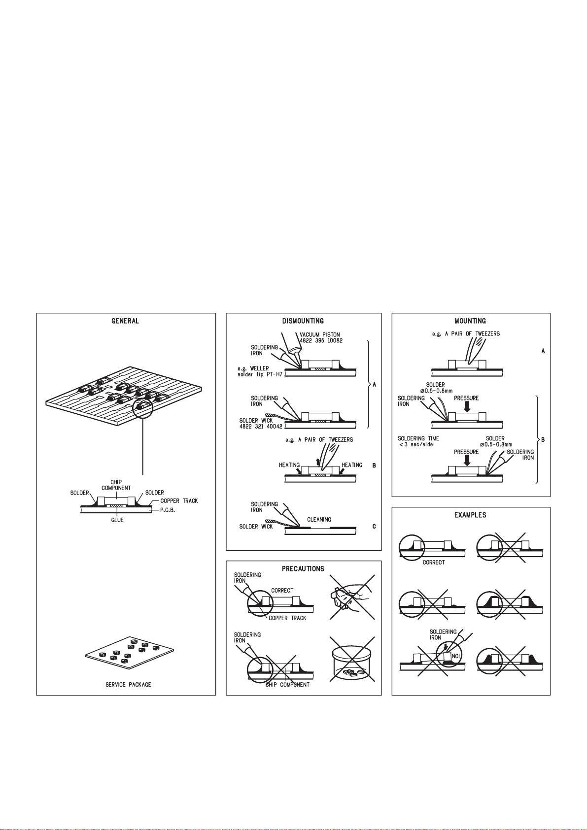
HANDLING CHIP COMPONENTS

1 - 5
NL
WAARSCHUWING
Alle IC’s en vele andere halfgeleiders zijn
gevoelig voor electrostatische ontladingen
(ESD).
Onzorgvuldig behandelen tijdens reparatie kan
de levensduur drastisch doen verminderen.
Zorg ervoor dat u tijdens reparatie via een
polsband met weerstand verbonden bent met
hetzelfde potentiaal als de massa van het
apparaat.
Houd componenten en hulpmiddelen ook op
ditzelfde potentiaal.
I
AVVERTIMENTO
Tutti IC e parecchi semi-conduttori sono
sensibili alle scariche statiche (ESD).
La loro longevità potrebbe essere fortemente
ridatta in caso di non osservazione della più
grande cauzione alla loro manipolazione.
Durante le riparazioni occorre quindi essere
collegato allo stesso potenziale che quello della
massa dell’apparecchio tramite un braccialetto
a resistenza.
Assicurarsi che i componenti e anche gli utensili
con quali si lavora siano anche a questo
potenziale.
GB
Safety regulations require that the set be restored to its original
condition and that parts which are identical with those specified,
be used.
Safety components are marked by the symbol
!
.
NL
Veiligheidsbepalingen vereisen, dat het apparaat bij reparatie in
zijn oorspronkelijke toestand wordt teruggebracht en dat onderdelen,
identiek aan de gespecificeerde, worden toegepast.
De Veiligheidsonderdelen zijn aangeduid met het symbol
!
.
F
Les normes de sécurité exigent que l’appareil soit remis à l’état
d’origine et que soient utiliséés les piéces de rechange identiques
à celles spécifiées.
Less composants de sécurité sont marqués
!
.
D
Bei jeder Reparatur sind die geltenden Sicherheitsvorschriften zu
beachten. Der Original zustand des Geräts darf nicht verändert werden;
für Reparaturen sind Original-Ersatzteile zu verwenden.
Sicherheitsbauteile sind durch das Symbol
!
markiert.
I
Le norme di sicurezza esigono che l’apparecchio venga rimesso
nelle condizioni originali e che siano utilizzati i pezzi di ricambio
identici a quelli specificati.
Componenty di sicurezza sono marcati con
!
.
GB
After servicing and before returning set to customer perform a leakage
current measurement test from all exposed metal parts to earth ground
to assure no shock hazard exist, The leakage current must not
exceed 0.5mA.
CLASS 1
LASER PRODUCT
3122 110 03420
GB
Warning !
Invisible laser radiation when open.
Avoid direct exposure to beam.
S
Varning !
Osynlig laserstrålning när apparaten är öppnad och spärren
är urkopplad. Betrakta ej strålen.
SF
Varoitus !
Avatussa laitteessa ja suojalukituksen ohitettaessa olet alttiina
näkymättömälle laserisäteilylle. Älä katso säteeseen!
GB
WARNING
All ICs and many other semi-conductors are
susceptible to electrostatic discharges (ESD).
Careless handling during repair can reduce life
drastically.
When repairing, make sure that you are
connected with the same potential as the mass
of the set via a wrist wrap with resistance.
Keep components and tools also at this
potential.
F
ATTENTION
Tous les IC et beaucoup d’autres
semi-conducteurs sont sensibles aux
décharges statiques (ESD).
Leur longévité pourrait être considérablement
écourtée par le fait qu’aucune précaution n’est
prise à leur manipulation.
Lors de réparations, s’assurer de bien être relié
au même potentiel que la masse de l’appareil et
enfiler le bracelet serti d’une résistance de
sécurité.
Veiller à ce que les composants ainsi que les
outils que l’on utilise soient également à ce
potentiel.
ESD
D
WARNUNG
Alle ICs und viele andere Halbleiter sind
empfindlich gegenüber elektrostatischen
Entladungen (ESD).
Unsorgfältige Behandlung im Reparaturfall kan
die Lebensdauer drastisch reduzieren.
Veranlassen Sie, dass Sie im Reparaturfall über
ein Pulsarmband mit Widerstand verbunden
sind mit dem gleichen Potential wie die Masse
des Gerätes.
Bauteile und Hilfsmittel auch auf dieses gleiche
Potential halten.
DK
Advarse !
Usynlig laserstråling ved åbning når sikkerhedsafbrydere er
ude af funktion. Undgå udsaettelse for stråling.
F
"Pour votre sécurité, ces documents doivent être utilisés par
des spécialistes agréés, seuls habilités à réparer votre
appareil en panne".
GB
ESD PROTECTION EQUIPMENT
Complete Kit ESD3 (small tablemat, wristband,
connection box, estention cable and earth cable ....... 4822 310 10671
Wristband tester ................................................................. 4822 344 13999

1 - 6
Pb(Lead) Free Solder
When soldering , be sure to use the pb free solder.
INDENTIFICATION:
Regardless of special logo (not always indicated)
one must treat all sets from 1 Jan 2005onwards, according
next rules:
Important note: In fact also products of year 2004 must
be treated in this way as long as you avoid mixing solder-
alloys (leaded/ lead-free). So best to always use SAC305
and the higher temperatures belong to this.
Due to lead-free technology some rules have to be
respected by the workshop during a repair:
• Use only lead-free solder alloy Philips SAC305 with
order code 0622 149 00106. If lead-free solder-paste
is required, please contact the manufacturer of your
solder-equipment. In general use of solder-paste
within workshops should be avoided because paste is
not easy to store and to handle.
• Use only adequate solder tools applicable for lead-
free solder alloy. The solder tool must be able
– To reach at least a solder-temperature of 400?C,
– To stabilize the adjusted temperature at the solder-
tip
– To exchange solder-tips for different applications.
• Adjust your solder tool so that a temperature around
360?C – 380?C is reached and stabilized at the solder
joint. Heating-time of the solder-joint should not exceed
~ 4 sec. Avoid temperatures above 400?C otherwise
wear-out of tips will rise drastically and flux-fluid will
be destroyed. To avoid wear-out of tips switch off un-
used equipment, or reduce heat.
• Mix of lead-free solder alloy / parts with leaded solder
alloy / parts is possible but PHILIPS recommends
strongly to avoid mixed solder alloy types (leaded and
lead-free).
If one cannot avoid or does not know whether product
is lead-free, clean carefully the solder-joint from old
solder alloy and re-solder with new solder alloy
(SAC305).
• Use only original spare-parts listed in the Service-
Manuals. Not listed standard-material (commodities)
has to be purchased at external companies.
• Special information for BGA-ICs:
– Always use the 12nc-recognizable soldering
temperature profile of the specific BGA (for de-
soldering always use the lead-free temperature profile,
in case of doubt)
– Lead free BGA-ICs will be delivered in so-called ‘dry-
packaging’ (sealed pack including a silica gel pack) to
protect the IC against moisture. After opening,
dependent of MSL-level seen on indicator-label in the
bag, the BGA-IC possibly still has to be baked dry.
(MSL=Moisture Sensitivity Level). This will be
communicated via AYS-website.
Do not re-use BGAs at all.
• For sets produced before 1.1.2005 (except products
of 2004), containing leaded solder-alloy and
components, all needed spare-parts will be available
till the end of the service-period. For repair of such
sets nothing changes.
• On our website www.atyourservice.ce.Philips.com
you find more information to:
• BGA-de-/soldering (+ baking instructions)
• Heating-profiles of BGAs and other ICs used in
Philips-sets
You will find this and more technical information
within the “magazine”, chapter “workshop news”.
For additional questions please contact your local
repair-helpdesk.
2 - 1 2 - 1
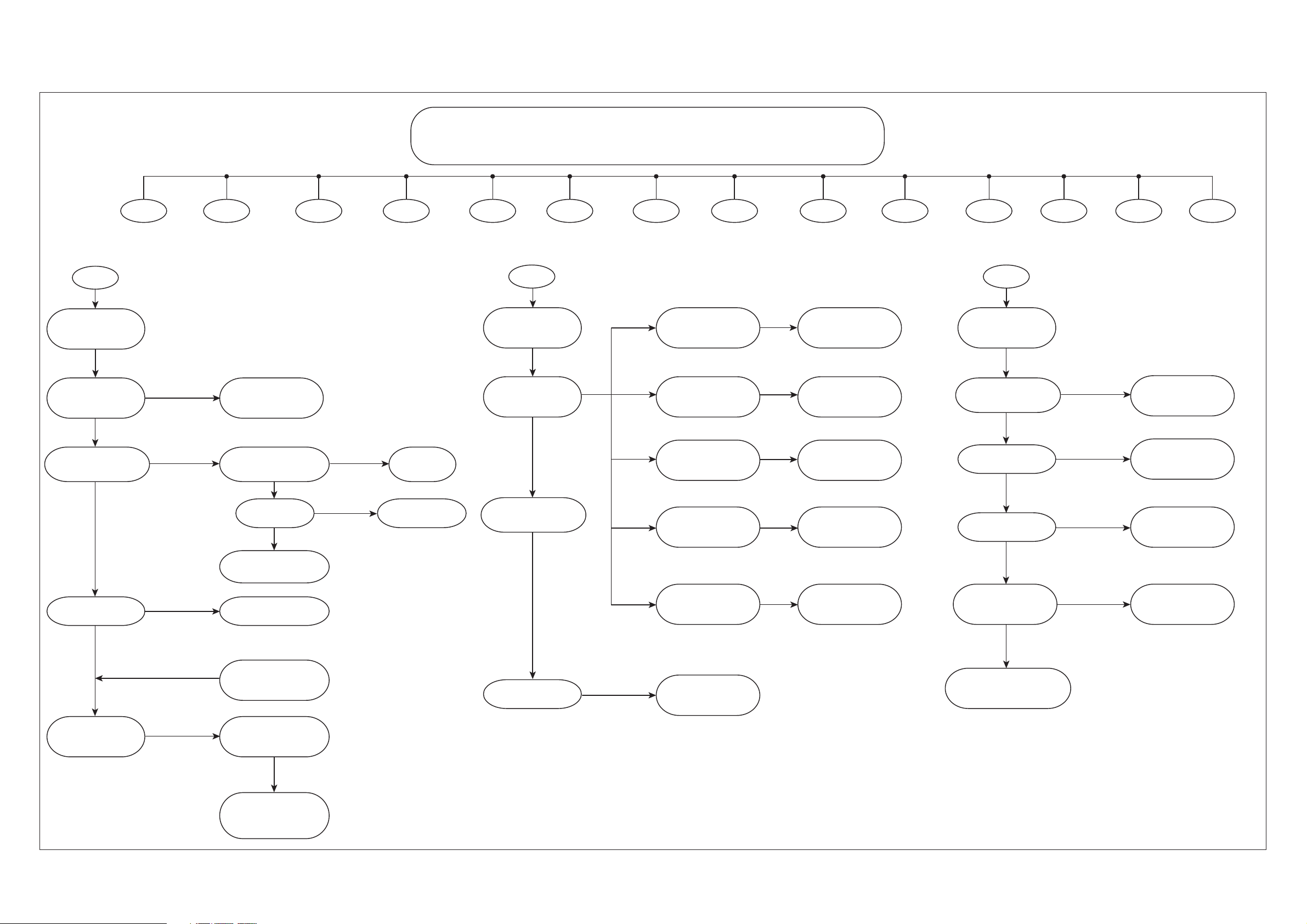
REPAIR INSTRUCTION (Part One)
MA IN UNIT REPAIR CHART 1/ 3
A
A ll function
No workin g
Check all sy stem
a ll cable is l oos e
or bad IN T
Pa nel stanby LE D
sh ow work in g or No t
Re -i nsert and fi x
the cabl e
Check back power
PC
B
F 901 bad cause da ma ge
Change F 901
Check CN905 2pin
BK 5V if righ t
Check repair control
PC B Standb y circui t
Check +5V power
supply circui t
Check RB 901 1pin
+5 V= 5V
Check repair switch
po wer ci rcuit ( See B)
Check all Voltage
3.3V and 1.8V
give circuit
V CC=5V
VD 33= 3.3V
VD 18= 1.8V
Check IC208 Pin234 OS C
frequenc y 27M Hz
Repair ma in pcb betw een
IC 202 IC 206 IC 208and IC 602
circui t
YE S
NO
NO
BA D
NO
OK
YE S
WORK
NO
CHECK
CORRECT
YE S
YE S
B
Power Supply
No workin g
A ll Vo lta ge
No Ou tput
Check F 901
Ba d Cause Damage
Check BK 5V +5V
Wo rking or No t
No
YE S
No
+ 35.5V Voltage
No Ou tput
Check Repair IC 901 IC 902
A nd It s co nn circui t
- 27V Voltage
No Ou tput
+ 12V Voltage
No Ou tput
+5 V Vo lta ge
No Ou tput
Check Q901 Q909 IC 901
A nd It s Co nj oi nt Part
Check Q912 IC 902
A nd It s Co nj oi nt Part
Check Q912 IC 902
A nd It s Co nj oi nt Part
Check Q912 IC 902
A nd It s Co nj oi nt Part
No
C
A ll Functio n
No S ound
Check PO WE R IC
Vo lta ge + 35.5V
Ye s
See Contents B
CheckQ306 D304 ZD303
A nd It s co nn part s
Ye s
No
Check Q305 C
Vo lta ge 3.3V
OK
No
A
A ll F unctio n
No Wo rkin g
B
Po wer Su
pply
No Wo rkin g
C
A ll F unctio n
No So und
D
Ip od inpu t
No So und
E
A udi o line IN
No Ou tput
F
Wi reless
No Ou tput
G
DVD A udi o
No So und
H
MP 3 In
No So und
I
CO AX IA L In
No So und
L
T uner No So und
M
No Sv ideo Output
O
HD MI No Ou tput
BK 5V Voltage
No Ou tput
Check Q912 IC 902
A nd It s Co nj oi nt Part
CheckQ501 Q502 IC 505
A nd It s co nn part s
OK
LO W
CheckQ902 ZD905 IC 505
A nd It s co nn part s
Check Q902 C
Vo lta ge 3.3V
OK
No
Check IC 505 51P IN
HIGH( 3.3V ) OR LO W( 0V )
Check IC 501 IC 502 IC 503 IC 504
A nd It s Co nj oi nt Part
P
No CVBS Ou tput
Q
No Y Pr Pb ou tput

2 - 2 2 - 2
MA IN UNIT REPAIR CHART 2/ 3
D
Ipod inpu t
No S ound
Check DOC K TO
HT S 3540 Cable IN T
Check ipod input pc b
JK 101CN 101 IN T OR NO
Change this Cable
Change this TW O
Check CN101 JK 101
Check DOC K
IN T
OK
IN T
OK
Check CN101 5P IN
Vo lta ge Correct is 5.0V
No
No
E
AUX/TV IN
No Output
Check JK 302
Check IC 304 IC 305 Pin7
IN T or No
approx -5.6V Pin16 approx +5.6 V
Check ZD301ZD302
Check FB 307 FB 308
Change this JK
Check IC 306
A nd It s Co nj oi nt part s
OK
No
OK
Check IC 306 Pin1 Pin3 6 13
Vo lta ge Correct is 5.0V
Ye s
IN T
No
F
Wi reless
No Output
OK or No
Check JK 401 IC 505
A nd Its conjoint part s
No
OK
Check JK 401
Pin1 approx +5 V
See B
G
DVD Audi o
No S ound
Check CN801 to
DVD loader Cable Loos e
No
OK
Check Open/Close
Wo rking or No t
Check CN802 CN803
Check IC 801
A nd It s co nj oi nt part s
No
Re -In sert and fi x
the cabl e
YE S
De term ine Picture Ou tput
OK
Check IC 208 An d
Th eir Conjoint Pa rt s
No
Check Q801 Q802 Q803
OK
H
I
C OAXIAL In
No S ound
IN T
OK
Check JK 702 Pin5
INT OR NO
RE PA IR ok
Check A nd Repair
FB 202 FB 203
No
Check IC 201 IC 208 A nd
OK
Check IC 201 Pin6 pin 23
approx +5.0V
See C
OK
Check JK 302
Check IC 304 IC 305 Pin7
IN T or No
approx -5.6V Pin16 approx +5.6 V
Check ZD301ZD302
Check FB 307 FB 308
Change this JK
Check IC 306
A nd It s Co nj oi nt part s
OK
No
OK
Check IC 306 Pin1 Pin3 6 13
Vo lta ge Correct is 5.0V
Ye s
IN T
No
See C
OK
OK
See C
or NO
Ye s or No
to DVD Lo ader Cable loos e
or Ba d IN T
or Ba d IN T
Ye s
Ye s or No
Q804 A nd Th eir Conjoint Pa rt s
It s Co nj oi nt Part s
Ye s or No
A nd It s Co nj oi nt part s
FB 309 Q 904
Ye s or No
FB 309 Q 904
REPAIR INSTRUCTION (Part Two)

2 - 3 2 - 3
REPAIR INSTRUCTION (Part Three)
MA IN UNIT REPAIR CHART 3/3
L
Tuner No Sound
Output
Check CN301 Pin9= +9V
Check CN301 Q901ZD904
No
And Its Conjoint Parts
Check SW Power
See B
Yes
Check CN1 to CN301
Cable Loose or IN T
Check CN1 Pin2/Clock
Pin3/Data,Pin4/CE
Affirm Correct
Yes
No
Check IC102 IC108
And Its Conjoint Part s
No
Check IC1 And
No
Its Conjoint Parts
Check VT Valtage
No
Low Freq=0.8--1.8V
Hi Freq=8.0--9.0V
Check IC1 OSC Input
Pin5---AM OSC
VT No Change
Pin3---FM OSC
Repair FM osc Section
And Its Conjoint Part s
No AMNo FM
L6 or DT4
Repair AM osc Section
And Its Conjoint Part s
L12 or DT5
Check Repair CN302 IC301
And Its Conjoint Part s
Check CN1 L12 CF3
And Its Conjoint Parts
OK
Check CN302 IC301
And Its Conjoint Parts
Check CF2 And
Its Conjoint Parts
L6 DT4
And Its Conjoint Part s
AM Function No Sound
FM Function No Sound
OK
OK
OK
OK
Check IC1 X1 C39
And Its Conjount Parts
OK
Check Main Pcb Of Tuner Input Circuit
M
No Svideo output
Check JK701 Pin1 Pin3
Video signal
Yes
Check IC208 PIN133 PIN140
To JK701 Conjoint Parts
O
HDMI No Output
Yes
Insert And Pull out HDMI
cable
See C
OK
CheckQ610 Q611 Q609
And Conjoint Parts
No
Check IC602 3.3V And 1.8V
Check Q203 Q204
And Conjoint Parts
No
OK
Check C300
CheckC300
And Conjoint Parts
No
OK
Check IC602 PIN72:ASPDIF
Check IC602 IC208
And Conjoint Part s
No
PIN77:ALCK
p
No CVBS output
Check JK701 Pin5
Video signal
Yes
Check IC208 PIN134
To JK701 Conjoint Parts
Q
No Y Pr Pb output
Check JK702 Pin12 Pin4
Pin5 Video signal
Yes
Check IC208 PIN137 PIN138
pin139 To JK702 Conjoint Parts
3 - 1 3 - 1
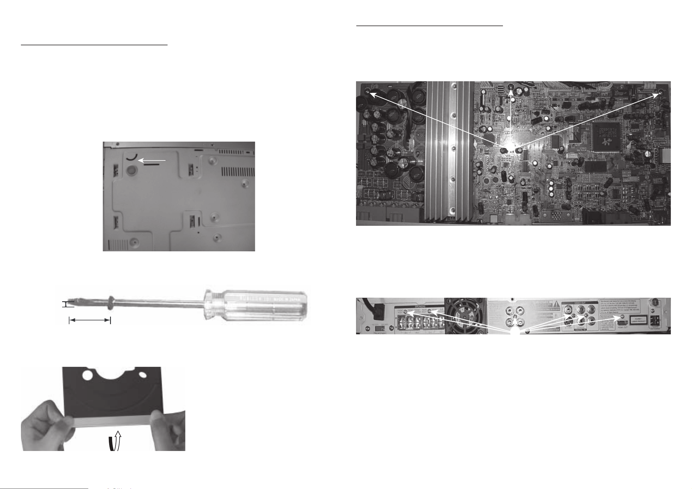
DISASSEMBLY INSTRUCTIONS
Dismantling of the Front Panel Assembly
1) Open the DVD Tray by using the Open/Close Button
while the Set is ON and disconnect the mains supply after
removing the Tray Cover.
Note: If this is not possible, the DVD Tray
has to be open manually.
Take a mini screw driver about 2mm diameter and make a
marking 24mm from the tip as shown in gure 2 . Place the
set on its side, insert the mini screw driver till the marking
and slide it towards the right as shown in gure 1 until the
Tray moves out of the Front Panel.
2) Return the set to its upright position and remove the Tray
Cover as shown in Figure 3 and close the tray manually by
pushing it back in.
3) Loosen 5 screws and remove the Top Cover by lifting the
rear portion upwards before sliding it out towards the rear.
- 3 screws on the back
- 1 screws each on the left & right side
4) Loosen 5 screws & lift up the top edge of Front Panel
assembly to free some catches before sliding it out towards
the front.
- 3 screws on the bottom
- 1 screw each on the left & right side
24mm
mm2
Figure 3
Figure 2
Dismantling of the Main PCB
2) Loosen 3 screw “ A “ on the top of main board as shown in
g ure 4.
1) Loosen 6 screw “B” at the back panel as shown in gure 5.
A
B
Figure 4
Figure 5
PULL
Figure 1
 Loading...