


NSC LM2940S-12, LM2940S-10, LM2940IMPX-9.0, LM2940IMPX-8.0, LM2940IMPX-5.0 Datasheet
...March 2000
LM2940/LM2940C
1A Low Dropout Regulator
General Description
The LM2940/LM2940C positive voltage regulator features the ability to source 1A of output current with a dropout voltage of typically 0.5V and a maximum of 1V over the entire temperature range. Furthermore, a quiescent current reduction circuit has been included which reduces the ground current when the differential between the input voltage and the output voltage exceeds approximately 3V. The quiescent current with 1A of output current and an input-output differential of 5V is therefore only 30 mA. Higher quiescent currents only exist when the regulator is in the dropout mode (VIN − V OUT ≤ 3V).
Designed also for vehicular applications, the LM2940/ LM2940C and all regulated circuitry are protected from reverse battery installations or 2-battery jumps. During line transients, such as load dump when the input voltage can
momentarily exceed the specified maximum operating voltage, the regulator will automatically shut down to protect both the internal circuits and the load. The LM2940/ LM2940C cannot be harmed by temporary mirror-image insertion. Familiar regulator features such as short circuit and thermal overload protection are also provided.
Features
nDropout voltage typically 0.5V @IO = 1A
nOutput current in excess of 1A
nOutput voltage trimmed before assembly
nReverse battery protection
nInternal short circuit current limit
nMirror image insertion protection
nP+ Product Enhancement tested
Typical Application
DS008822-3
*Required if regulator is located far from power supply filter.
**COUT must be at least 22 µF to maintain stability. May be increased without bound to maintain regulation during transients. Locate as close as possible to the regulator. This capacitor must be rated over the same operating temperature range as the regulator and the ESR is critical; see curve.
Ordering Information
Temperature |
|
|
Output Voltage |
|
|
Package |
||
|
Range |
|
|
|
|
|
|
|
|
5.0 |
8.0 |
9.0 |
10 |
12 |
15 |
|
|
|
|
|
|
|
|
|
|
|
0ÊC ≤ TJ ≤ 125ÊC |
LM2940CT-5.0 |
|
LM2940CT-9.0 |
|
LM2940CT-12 |
LM2940CT-15 |
TO-220 |
|
|
|
LM2940CS-5.0 |
|
LM2940CS-9.0 |
|
LM2940CS-12 |
LM2940CS-15 |
TO-263 |
|
|
|
|
|
|
|
|
|
−40ÊC |
≤ TJ ≤ 125ÊC |
LM2940T-5.0 |
LM2940T-8.0 |
LM2940T-9.0 |
LM2940T-10 |
LM2940T-12 |
|
TO-220 |
|
|
LM2940S-5.0 |
LM2940S-8.0 |
LM2940S-9.0 |
LM2940S-10 |
LM2940S-12 |
|
TO-263 |
|
|
|
|
|
|
|
|
|
−40ÊC |
≤ TJ ≤ 85ÊC |
LM2940IMP-5.0 |
LM2940IMP-8.0 |
LM2940IMP-9.0 |
LM2940IMP-10 |
LM2940IMP-12 |
LM2940IMP-15 |
SOT-223 |
|
|
LM2940IMPX-5.0 |
LM2940IMPX-8.0 |
LM2940IMPX-9.0 |
LM2940IMPX-10 |
LM2940IMPX-12 |
LM2940IMPX-15 |
SOT-223 |
|
|
|
|
|
|
|
|
in Tape |
|
|
|
|
|
|
|
|
and Reel |
|
|
|
|
|
|
|
|
|
SOT-223 Package |
L53B |
L54B |
L0EB |
L55B |
L56B |
L70B |
|
|
|
Marking |
|
|
|
|
|
|
|
|
|
|
|
|
|
|
|
|
The physical size of the SOT-223 is too small to contain the full device part number. The package markings indicated are what will appear on the actual device.
Temperature |
|
Output Voltage |
|
Package |
|
Range |
|
|
|
|
|
5.0 |
8.0 |
12 |
15 |
|
|
|
|
|
|
|
|
−55ÊC ≤ TJ ≤ 125ÊC |
LM2940J-5.0/883 |
LM2940J-8.0/883 |
LM2940J-12/883 |
LM2940J-15/883 |
J16A |
|
5962-8958701EA |
5962-9088301QEA |
5962-9088401QEA |
5962-9088501QEA |
|
|
LM2940WG5.0/883 |
|
|
|
WG16A |
|
5962-8958701XA |
|
|
|
|
|
|
|
|
|
|
For information on military temperature range products, please go to the Mil/Aero Web Site at http://www.national.com/appinfo/milaero/index.html.
Regulator Dropout Low 1A LM2940/LM2940C
© 2000 National Semiconductor Corporation |
DS008822 |
www.national.com |
LM2940/LM2940C
Connection Diagrams
(TO-220) Plastic Package
DS008822-2
Front View
Order Number LM2940CT-5.0, LM2940CT-9.0,
LM2940CT-12, LM2940CT-15, LM2940T-5.0,
LM2940T-8.0, LM2940T-9.0,
LM2940T-10 or LM2940T-12
See NS Package Number TO3B
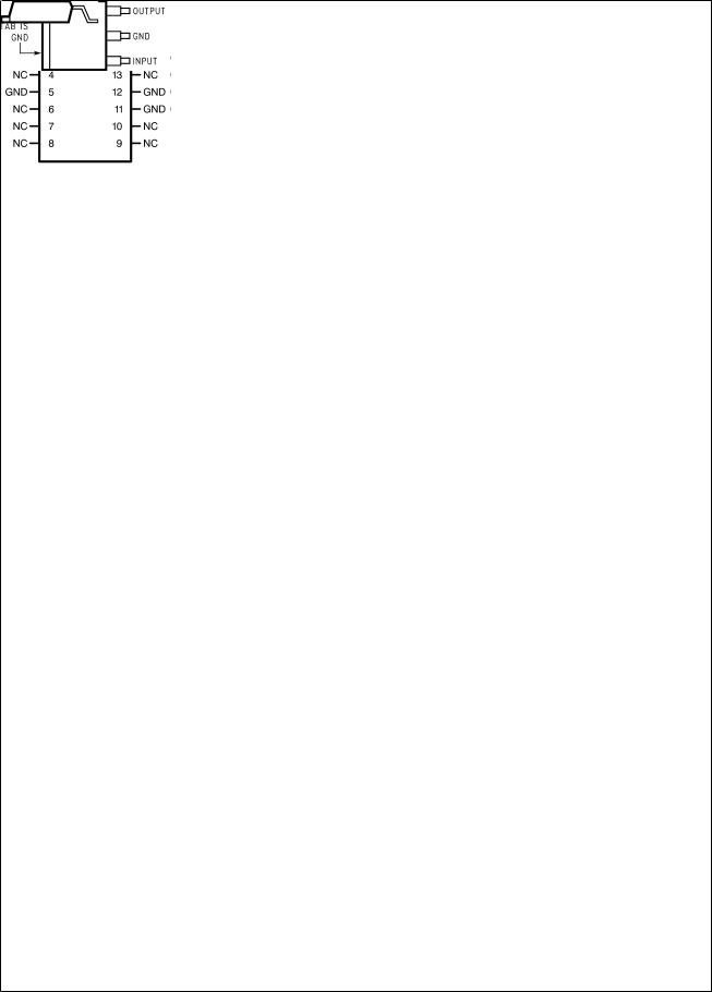
16-Lead Dual-in-Line Package (J)
DS008822-43
Top View
Order Number LM2940J-5.0/883 (5962-8958701EA),
LM2940J-8.0/883 (5962-9088301QEA),
LM2940J-12/883 (5962-9088401QEA),
LM2940J-15/883 (5962-9088501QEA)
See NS Package Number J16A
(TO-263) Surface-Mount Package
DS008822-11
Top View
DS008822-12
Side View
Order Number LM2940CS-5.0, LM2940CS-9.0,
LM2940CS-12, LM2940CS-15,
LM2940S-5.0, LM2940S-8.0,
LM2940S-9.0, LM2940S-10 or LM2940S-12
See NS Package Number TS3B
3-Lead SOT-223
DS008822-42
Front View
Order Part Number LM2940IMP-5.0,
LM2940IMP-8.0, LM2940IMP-9.0, LM2940IMP-10, LM2940IMP-12 or LM2940IMP-15 See NS Package Number MP04A
16-Lead Ceramic Surface-Mount Package (WG)
DS008822-44
Top View
Order Number LM2940WG5.0/883 (5962-8958701XA)
See NS Package Number WG16A
www.national.com |
2 |

Absolute Maximum Ratings (Note 1)
If Military/Aerospace specified devices are required, please contact the National Semiconductor Sales Office/ Distributors for availability and specifications.
LM2940S, T, MP ≤ 100 ms |
60V |
LM2940CS, T ≤ 1 ms |
45V |
Internal Power Dissipation |
|
(Note 2) |
Internally Limited |
Maximum Junction Temperature |
150ÊC |
Storage Temperature Range |
−65ÊC ≤ TJ ≤ +150ÊC |
Lead Temperature, Time for Wave Soldering |
|
TO-220 (T) Package |
260ÊC, 10s |
TO-263 (S) Package |
260ÊC, 4s |
SOT-223 (MP) Package |
260ÊC, 4s |
ESD Susceptibility (Note 3) |
2 kV |
Operating Conditions (Note 1)
Input Voltage |
|
26V |
Temperature Range |
|
|
LM2940T, LM2940S |
−40ÊC |
≤ TJ ≤ 125ÊC |
LM2940CT, LM2940CS |
0ÊC ≤ TJ ≤ 125ÊC |
|
LM2940IMP |
−40ÊC |
≤ TJ ≤ 85ÊC |
LM2940J, LM2940WG |
−55ÊC |
≤ TJ ≤ 125ÊC |
Electrical Characteristics
VIN = VO + 5V, IO = 1A, CO = 22 µF, unless otherwise specified. Boldface limits apply over the entire operating temperature range of the indicated device. All other specifications apply for TA = TJ = 25ÊC.
Output Voltage (VO) |
|
5V |
|
|
8V |
|
|
||
|
|
|
LM2940 |
LM2940/883 |
|
LM2940 |
LM2940/883 |
Units |
|
Parameter |
Conditions |
Typ |
Limit |
Limit |
Typ |
Limit |
Limit |
||
|
|||||||||
|
|
|
(Note 4) |
(Note 5) |
|
(Note 4) |
(Note 5) |
|
|
|
|
|
|
|
|
|
|
|
|
|
|
|
6.25V ≤ VIN ≤ 26V |
|
9.4V ≤ VIN ≤ 26V |
|
|||
Output Voltage |
5 mA ≤ IO ≤ 1A |
5.00 |
4.85/4.75 |
4.85/4.75 |
8.00 |
7.76/7.60 |
7.76/7.60 |
VMIN |
|
|
|
|
5.15/5.25 |
5.15/5.25 |
|
8.24/8.40 |
8.24/8.40 |
VMAX |
|
Line Regulation |
VO + 2V ≤ VIN ≤ 26V, |
20 |
50 |
40/50 |
20 |
80 |
50/80 |
mVMAX |
|
|
IO = 5 mA |
|
|
|
|
|
|
|
|
Load Regulation |
50 mA ≤ IO ≤ 1A |
|
|
|
|
|
|
|
|
|
LM2940, LM2940/883 |
35 |
50/80 |
50/100 |
55 |
80/130 |
80/130 |
mVMAX |
|
|
LM2940C |
35 |
50 |
|
55 |
80 |
|
|
|
|
|
|
|
|
|
|
|
|
|
Output |
100 mADC and |
|
|
|
|
|
|
|
|
Impedance |
20 mArms, |
35 |
|
1000/1000 |
55 |
|
1000/1000 |
mΩ |
|
|
fO = 120 Hz |
|
|
|
|
|
|
|
|
Quiescent |
VO +2V ≤ VIN ≤ 26V, |
|
|
|
|
|
|
|
|
Current |
IO = 5 mA |
|
|
|
|
|
|
|
|
|
LM2940, LM2940/883 |
10 |
15/20 |
15/20 |
10 |
15/20 |
15/20 |
mAMAX |
|
|
LM2940C |
10 |
15 |
|
|
|
|
|
|
|
|
|
|
|
|
|
|
|
|
|
VIN = VO + 5V, |
30 |
45/60 |
50/60 |
30 |
45/60 |
50/60 |
mAMAX |
|
|
IO = 1A |
|
|
|
|
|
|
|
|
Output Noise |
10 Hz − 100 kHz, |
150 |
|
700/ 700 |
240 |
|
1000/1000 |
µVrms |
|
Voltage |
IO = 5 mA |
|
|
|
|
|
|
|
|
Ripple Rejection |
fO = 120 Hz, 1 Vrms, |
|
|
|
|
|
|
|
|
|
IO = 100 mA |
|
|
|
|
|
|
|
|
|
LM2940 |
72 |
60/54 |
|
66 |
54/48 |
|
dBMIN |
|
|
LM2940C |
72 |
60 |
|
66 |
54 |
|
|
|
|
|
|
|
|
|
|
|
|
|
|
fO = 1 kHz, 1 Vrms, |
|
|
60/50 |
|
|
54/48 |
dBMIN |
|
|
IO = 5 mA |
|
|
|
|
|
|
|
|
Long Term |
|
20 |
|
|
32 |
|
|
mV/ |
|
Stability |
|
|
|
|
|
|
|
1000 Hr |
|
|
|
|
|
|
|
|
|
|
|
Dropout Voltage |
IO = 1A |
0.5 |
0.8/1.0 |
0.7/1.0 |
0.5 |
0.8/1.0 |
0.7/1.0 |
VMAX |
|
|
IO = 100 mA |
110 |
150/200 |
150/200 |
110 |
150/200 |
150/200 |
mVMAX |
|
Short Circuit |
(Note 6) |
1.9 |
1.6 |
1.5/1.3 |
1.9 |
1.6 |
1.6/1.3 |
AMIN |
|
Current |
|
||||||||
|
|
|
|
|
|
|
|
||
|
|
|
|
|
|
|
|
|
|
LM2940/LM2940C
3 |
www.national.com |

LM2940/LM2940C
Electrical Characteristics (Continued)
VIN = VO + 5V, IO = 1A, CO = 22 µF, unless otherwise specified. Boldface limits apply over the entire operating temperature range of the indicated device. All other specifications apply for TA = TJ = 25ÊC.
Output Voltage (VO) |
|
5V |
|
|
8V |
|
|
||
|
|
|
LM2940 |
LM2940/883 |
|
LM2940 |
LM2940/883 |
Units |
|
Parameter |
Conditions |
Typ |
Limit |
Limit |
Typ |
Limit |
Limit |
||
|
|||||||||
|
|
|
(Note 4) |
(Note 5) |
|
(Note 4) |
(Note 5) |
|
|
|
|
|
|
|
|
|
|
|
|
Maximum Line |
RO = 100Ω |
|
|
|
|
|
|
|
|
Transient |
LM2940, T ≤ 100 ms |
75 |
60/60 |
|
75 |
60/60 |
|
VMIN |
|
|
LM2940/883, T ≤ 20 ms |
|
|
40/40 |
|
|
40/40 |
||
|
|
|
|
|
|
||||
|
LM2940C, T ≤ 1 ms |
55 |
45 |
|
55 |
45 |
|
|
|
|
|
|
|
|
|
|
|
|
|
Reverse Polarity |
RO = 100Ω |
|
|
|
|
|
|
|
|
DC Input Voltage |
LM2940, LM2940/883 |
−30 |
−15/ −15 |
−15/ −15 |
−30 |
−15/ −15 |
−15/ −15 |
VMIN |
|
|
LM2940C |
−30 |
−15 |
|
−30 |
−15 |
|
|
|
|
|
|
|
|
|
|
|
|
|
Reverse Polarity |
RO = 100Ω |
|
|
|
|
|
|
|
|
Transient Input |
LM2940, T ≤ 100 ms |
−75 |
−50/ −50 |
|
−75 |
−50/ −50 |
|
VMIN |
|
Voltage |
LM2940/883, T ≤ 20 ms |
|
|
−45/ −45 |
|
|
−45/ −45 |
|
|
|
LM2940C, T ≤ 1 ms |
−55 |
−45/ −45 |
|
|
|
|
|
|
|
|
|
|
|
|
|
|
|
|
Electrical Characteristics
VIN = VO + 5V, IO = 1A, CO = 22 µF, unless otherwise specified. Boldface limits apply over the entire operating temperature range of the indicated device. All other specifications apply for TA = TJ = 25ÊC.
Output Voltage (VO) |
|
9V |
|
10V |
|
||
|
|
|
LM2940 |
|
LM2940 |
Units |
|
Parameter |
Conditions |
Typ |
Limit |
Typ |
Limit |
||
|
|||||||
|
|
|
(Note 4) |
|
(Note 4) |
|
|
|
|
|
|
|
|
|
|
|
|
10.5V ≤ VIN ≤ 26V |
11.5V ≤ VIN ≤ 26V |
|
|||
Output Voltage |
5 mA ≤ IO ≤1A |
9.00 |
8.73/8.55 |
10.00 |
9.70/9.50 |
VMIN |
|
|
|
|
9.27/9.45 |
|
10.30/10.50 |
VMAX |
|
Line Regulation |
VO + 2V ≤ VIN ≤ 26V, |
20 |
90 |
20 |
100 |
mVMAX |
|
|
IO = 5 mA |
|
|
|
|
|
|
Load Regulation |
50 mA ≤ IO ≤ 1A |
|
|
|
|
|
|
|
LM2940 |
60 |
90/150 |
65 |
100/165 |
mVMAX |
|
|
LM2940C |
60 |
90 |
|
|
|
|
|
|
|
|
|
|
|
|
Output Impedance |
100 mADC and |
|
|
|
|
|
|
|
20 mArms, |
60 |
|
65 |
|
mΩ |
|
|
fO = 120 Hz |
|
|
|
|
|
|
Quiescent |
VO +2V ≤ VIN < 26V, |
|
|
|
|
|
|
Current |
IO = 5 mA |
|
|
|
|
|
|
|
LM2940 |
10 |
15/20 |
10 |
15/20 |
mAMAX |
|
|
LM2940C |
10 |
15 |
|
|
|
|
|
|
|
|
|
|
|
|
|
VIN = VO + 5V, IO = 1A |
30 |
45/60 |
30 |
45/60 |
mAMAX |
|
Output Noise |
10 Hz − 100 kHz, |
270 |
|
300 |
|
µV rms |
|
Voltage |
IO = 5 mA |
|
|
|
|
|
|
Ripple Rejection |
fO = 120 Hz, 1 Vrms, |
|
|
|
|
|
|
|
IO = 100 mA |
|
|
|
|
|
|
|
LM2940 |
64 |
52/46 |
63 |
51/45 |
dBMIN |
|
|
LM2940C |
64 |
52 |
|
|
|
|
|
|
|
|
|
|
|
|
Long Term |
|
34 |
|
36 |
|
mV/ |
|
Stability |
|
|
|
|
|
1000 Hr |
|
|
|
|
|
|
|
|
|
Dropout Voltage |
IO = 1A |
0.5 |
0.8/1.0 |
0.5 |
0.8/1.0 |
VMAX |
|
|
IO = 100 mA |
110 |
150/200 |
110 |
150/200 |
mVMAX |
|
www.national.com |
4 |

Electrical Characteristics (Continued)
VIN = VO + 5V, IO = 1A, CO = 22 µF, unless otherwise specified. Boldface limits apply over the entire operating temperature range of the indicated device. All other specifications apply for TA = TJ = 25ÊC.
Output Voltage (VO) |
|
9V |
|
10V |
|
||
|
|
|
LM2940 |
|
LM2940 |
Units |
|
Parameter |
Conditions |
Typ |
Limit |
Typ |
Limit |
||
|
|||||||
|
|
|
(Note 4) |
|
(Note 4) |
|
|
|
|
|
|
|
|
|
|
Short Circuit |
(Note 6) |
1.9 |
1.6 |
1.9 |
1.6 |
AMIN |
|
Current |
|
|
|
|
|
|
|
|
|
|
|
|
|
|
|
Maximum Line |
RO = 100Ω |
|
|
|
|
|
|
Transient |
T ≤ 100 ms |
|
|
|
|
|
|
|
LM2940 |
75 |
60/60 |
75 |
60/60 |
VMIN |
|
|
LM2940C |
55 |
45 |
|
|
|
|
|
|
|
|
|
|
|
|
Reverse Polarity |
RO = 100Ω |
|
|
|
|
|
|
DC Input Voltage |
LM2940 |
−30 |
−15/ −15 |
−30 |
−15/ −15 |
VMIN |
|
|
LM2940C |
−30 |
−15 |
|
|
|
|
|
|
|
|
|
|
|
|
Reverse Polarity |
RO = 100Ω |
|
|
|
|
|
|
Transient Input |
T ≤ 100 ms |
|
|
|
|
|
|
Voltage |
LM2940 |
−75 |
−50/ −50 |
−75 |
−50/ −50 |
VMIN |
|
|
LM2940C |
−55 |
−45/ −45 |
|
|
|
|
|
|
|
|
|
|
|
|
Electrical Characteristics
VIN = VO + 5V, IO = 1A, CO = 22 µF, unless otherwise specified. Boldface limits apply over the entire operating temperature range of the indicated device. All other specifications apply for TA = TJ = 25ÊC.
Output Voltage (VO) |
|
12V |
|
|
15V |
|
|
||
|
|
|
LM2940 |
LM2940/833 |
|
LM2940 |
LM2940/833 |
Units |
|
Parameter |
Conditions |
Typ |
Limit |
Limit |
Typ |
Limit |
Limit |
||
|
|||||||||
|
|
|
(Note 4) |
(Note 5) |
|
(Note 4) |
(Note 5) |
|
|
|
|
|
|
|
|
|
|
|
|
|
|
|
13.6V ≤ VIN ≤ 26V |
|
16.75V ≤ VIN ≤ 26V |
|
|||
Output Voltage |
5 mA ≤ IO ≤1A |
12.00 |
11.64/11.40 |
11.64/11.40 |
15.00 |
14.55/14.25 |
14.55/14.25 |
VMIN |
|
|
|
|
12.36/12.60 |
12.36/12.60 |
|
15.45/15.75 |
15.45/15.75 |
VMAX |
|
Line Regulation |
VO + 2V ≤ VIN ≤ 26V, |
20 |
120 |
75/120 |
20 |
150 |
95/150 |
mVMAX |
|
|
IO = 5 mA |
|
|
|
|
|
|
|
|
Load Regulation |
50 mA ≤ IO ≤ 1A |
|
|
|
|
|
|
|
|
|
LM2940, LM2940/883 |
55 |
120/200 |
120/190 |
|
|
150/240 |
mVMAX |
|
|
LM2940C |
55 |
120 |
|
70 |
150 |
|
|
|
|
|
|
|
|
|
|
|
|
|
Output |
100 mADC and |
|
|
|
|
|
|
|
|
Impedance |
20 mArms, |
80 |
|
1000/1000 |
100 |
|
1000/1000 |
mΩ |
|
|
fO = 120 Hz |
|
|
|
|
|
|
|
|
Quiescent |
VO +2V ≤ VIN ≤ 26V, |
|
|
|
|
|
|
|
|
Current |
IO = 5 mA |
|
|
|
|
|
|
|
|
|
LM2940, LM2940/883 |
10 |
15/20 |
15/20 |
|
|
15/20 |
mAMAX |
|
|
LM2940C |
10 |
15 |
|
10 |
15 |
|
|
|
|
|
|
|
|
|
|
|
|
|
|
VIN = VO + 5V, IO = 1A |
30 |
45/60 |
50/60 |
30 |
45/60 |
50/60 |
mAMAX |
|
Output Noise |
10 Hz − 100 kHz, |
360 |
|
1000/ 1000 |
450 |
|
1000/1000 |
µVrms |
|
Voltage |
IO = 5 mA |
|
|
|
|
|
|
|
|
Ripple Rejection |
fO = 120 Hz, 1 Vrms, |
|
|
|
|
|
|
|
|
|
IO = 100 mA |
|
|
|
|
|
|
|
|
|
LM2940 |
66 |
54/48 |
|
|
|
|
dBMIN |
|
|
LM2940C |
66 |
54 |
|
64 |
52 |
|
|
|
|
|
|
|
|
|
|
|
|
|
|
fO = 1 kHz, 1 Vrms, |
|
|
52/46 |
|
|
48/42 |
dBMIN |
|
|
IO = 5 mA |
|
|
|
|
|
|||
|
|
|
|
|
|
|
|
||
LM2940/LM2940C
5 |
www.national.com |

LM2940/LM2940C
Electrical Characteristics (Continued)
VIN = VO + 5V, IO = 1A, CO = 22 µF, unless otherwise specified. Boldface limits apply over the entire operating temperature range of the indicated device. All other specifications apply for TA = TJ = 25ÊC.
Output Voltage (VO) |
|
12V |
|
|
15V |
|
|
||
|
|
|
LM2940 |
LM2940/833 |
|
LM2940 |
LM2940/833 |
Units |
|
Parameter |
Conditions |
Typ |
Limit |
Limit |
Typ |
Limit |
Limit |
||
|
|||||||||
|
|
|
(Note 4) |
(Note 5) |
|
(Note 4) |
(Note 5) |
|
|
|
|
|
|
|
|
|
|
|
|
Long Term |
|
48 |
|
|
60 |
|
|
mV/ |
|
Stability |
|
|
|
|
|
1000 Hr |
|||
|
|
|
|
|
|
|
|||
|
|
|
|
|
|
|
|
|
|
Dropout Voltage |
IO = 1A |
0.5 |
0.8/1.0 |
0.7/1.0 |
0.5 |
0.8/1.0 |
0.7/1.0 |
VMAX |
|
|
IO = 100 mA |
110 |
150/200 |
150/200 |
110 |
150/200 |
150/200 |
mVMAX |
|
Short Circuit |
(Note 6) |
1.9 |
1.6 |
1.6/1.3 |
1.9 |
1.6 |
1.6/1.3 |
AMIN |
|
Current |
|
||||||||
|
|
|
|
|
|
|
|
||
|
|
|
|
|
|
|
|
|
|
Maximum Line |
RO = 100Ω |
|
|
|
|
|
|
|
|
Transient |
LM2940, T ≤ 100 ms |
75 |
60/60 |
|
|
|
|
|
|
|
LM2940/883, T ≤ 20 ms |
|
|
40/40 |
|
|
40/40 |
VMIN |
|
|
LM2940C, T ≤ 1 ms |
55 |
45 |
|
55 |
45 |
|
|
|
|
|
|
|
|
|
|
|
|
|
Reverse Polarity |
RO = 100Ω |
|
|
|
|
|
|
|
|
DC Input |
LM2940, LM2940/883 |
−30 |
−15/ −15 |
−15/ −15 |
|
|
−15/ −15 |
VMIN |
|
Voltage |
LM2940C |
−30 |
−15 |
|
−30 |
−15 |
|
|
|
|
|
|
|
|
|
|
|
|
|
Reverse Polarity |
RO = 100Ω |
|
|
|
|
|
|
|
|
Transient Input |
LM2940, T ≤ 100 ms |
−75 |
−50/ −50 |
|
|
|
|
|
|
Voltage |
LM2940/883, T ≤ 20 ms |
|
|
−45/ −45 |
|
|
−45/ −45 |
VMIN |
|
|
LM2940C, T ≤ 1 ms |
−55 |
−45/ −45 |
|
−55 |
−45/ −45 |
|
|
|
|
|
|
|
|
|
|
|
|
|
Note 1: Absolute Maximum Ratings are limits beyond which damage to the device may occur. Operating Conditions are conditions under which the device functions but the specifications might not be guaranteed. For guaranteed specifications and test conditions see the Electrical Characteristics.
Note 2: The maximum allowable power dissipation is a function of the maximum junction temperature, TJ, the junction-to-ambient thermal resistance, θJ−A , and the ambient temperature, TA. Exceeding the maximum allowable power dissipation will cause excessive die temperature, and the regulator will go into thermal shutdown.
The value of θJ−A (for devices in still air with no heatsink) is 60ÊC/W for the TO-220 package, 80ÊC/W for the TO-263 package, and 174ÊC/W for the SOT-223 package. The effective value of θJ−A can be reduced by using a heatsink (see Application Hints for specific information on heatsinking). The values of θJ−A and θJ−C for the K02A
package are 39ÊC/W and 4ÊC/W respectively.
Note 3: ESD rating is based on the human body model, 100 pF discharged through 1.5 kΩ.
Note 4: All limits are guaranteed at TA = TJ = 25ÊC only (standard typeface) or over the entire operating temperature range of the indicated device (boldface type). All limits at TA = TJ = 25ÊC are 100% production tested. All limits at temperature extremes are guaranteed via correlation using standard Statistical Quality Control methods.
Note 5: All limits are guaranteed at TA = TJ = 25ÊC only (standard typeface) or over the entire operating temperature range of the indicated device (boldface type). All limits are 100% production tested and are used to calculate Outgoing Quality Levels.
Note 6: Output current will decrease with increasing temperature but will not drop below 1A at the maximum specified temperature.
Typical Performance Characteristics
Dropout Voltage |
Dropout Voltage |
Output Voltage |
|
vs Temperature |
vs Temperature |
DS008822-13
DS008822-14 |
DS008822-15 |
www.national.com |
6 |
 Loading...