


LT3014HVES5
FEATURES
■VIN Range: 0.9V to 10V
■Minimum Input Voltage: 0.9V
■Dropout Voltage: 150mV Typical
■Output Current: 100mA
■Adjustable Output (VREF = VOUT(MIN) = 200mV)
■Fixed Output Voltages: 1.2V, 1.5V, 1.8V
■Stable with Low ESR, Ceramic Output Capacitors (2.2µF Minimum)
■0.2% Load Regulation from 1mA to 100mA
■Quiescent Current: 120µA (Typ)
■3µA Typical Quiescent Current in Shutdown
■Current Limit Protection
■Reverse-Battery Protection
■No Reverse Current
■Thermal Limiting with Hysteresis
■8-Lead DFN (3mm × 3mm) and MSOP Packages
APPLICATIOUS
■Low Current Regulators
■Battery-Powered Systems
■Cellular Phones
■Pagers
■Wireless Modems
TYPICAL APPLICATIOU
1.8V to 1.5V, 100mA VLDO Regulator
VIN |
|
|
|
|
|
|
|
|
|
|
|
IN |
|
|
|
|
|
|
|
|
OUT |
|
|
|
|
|
|
|
|
|
|
VOUT |
|
|
|
|
|
|
|
|
|
|
|
|
|
|
|
|
|
|
|
|
|
|
|
|
|
|
|
|
|
1.5V |
|||
1.8V |
|
|
|
|
|
|
|
LT3020-1.5 |
|
|
|
|
|
|
|
|
|
2.2 F 100mA |
||||||||||||||
|
|
|
|
|
|
|
|
|
|
2.2 F |
|
|
|
|
|
|
|
|
|
|
|
|||||||||||
|
|
|
|
|
|
|
|
|
|
|
|
|
|
|
|
|
|
|
|
|
||||||||||||
|
|
|
|
|
|
|
|
|
|
|
|
|
|
|
|
|
|
|
|
|
|
|
|
|||||||||
|
|
|
|
|
|
|
|
|
|
|
|
SHDN |
GND |
|
|
|
|
|
|
|
|
|
|
|
||||||||
|
|
|
|
|
|
|
|
|
|
|
|
|
|
|
|
|
|
|
|
|
|
|
|
|
||||||||
|
|
|
|
|
|
|
|
|
|
|
|
|
|
3020 TA01 |
||||||||||||||||||
|
|
|
|
|
|
|
|
|
|
|
|
|
|
|
|
|
|
|
|
|
|
|||||||||||
|
|
|
|
|
|
|
|
|
|
|
|
|
|
|
|
|
|
|
|
|
|
|||||||||||
|
|
|
|
|
|
|
|
|
|
|
|
|
|
|
|
|
|
|
|
|
|
|||||||||||
100mA, Low Voltage,
Very Low Dropout
Linear Regulator
DESCRIPTIOU
The LT®3020 is a very low dropout voltage (VLDOTM) linear regulator that operates from input supplies down to 0.9V. This device supplies 100mA of output current with a typical dropout voltage of 150mV. The LT3020 is ideal for low input voltage to low output voltage applications, providing comparable electrical efficiency to that of a switching regulator.
The LT3020 regulator optimizes stability and transient response with low ESR, ceramic output capacitors as small as 2.2µF. Other LT3020 features include 0% typical line regulation and 0.2% typical load regulation. In shutdown, quiescent current drops to 3µA.
Internal protection circuitry includes reverse-battery protection, current limiting, thermal limiting with hysteresis, and reverse-current protection. The LT3020 is available as an adjustable output device with an output range down to the 200mV reference. Three fixed output voltages, 1.2V, 1.5V and 1.8V, are also available.
The LT3020 regulator is available in the low profile (0.75mm) 8-lead (3mm × 3mm) DFN package with Exposed Pad and the 8-lead MSOP package.
 , LTC and LT are registered trademarks of Linear Technology Corporation. VLDO is a trademark of Linear Technology Corporation.
All other trademarks are the property of their respective owners.
Minimum Input Voltage
1.1
IL = 100mA
|
1.0 |
|
|
|
|
|
|
|
|
|
|
|
|
|
|
|
|
|
|
|
|
|
|
(V) |
0.9 |
|
|
|
|
|
|
|
|
|
|
|
|
|
|
|
|
|
|
|
|
||
|
|
|
|
|
|
|
|
|
|
|
|
VOLTAGE |
0.8 |
|
|
|
|
|
|
|
|
|
|
|
|
|
|
|
|
|
|
|
|
|
|
|
0.7 |
|
|
|
|
|
|
|
|
|
|
|
|
|
|
|
|
|
|
|
|
|
|
INPUT |
0.6 |
|
|
|
|
|
|
|
|
|
|
|
|
|
|
|
|
|
|
|
|
||
0.5 |
|
|
|
|
|
|
|
|
|
|
|
MINIMUM |
|
|
|
|
|
|
|
|
|
|
|
0.4 |
|
|
|
|
|
|
|
|
|
|
|
|
|
|
|
|
|
|
|
|
|
|
|
|
0.3 |
|
|
|
|
|
|
|
|
|
|
|
|
|
|
|
|
|
|
|
|
|
|
|
0.2 |
|
|
|
|
|
|
|
|
|
|
|
|
|
|
|
|
|
|
|
|
|
|
|
0.1 |
|
|
|
|
|
|
|
|
|
|
|
|
|
|
|
|
|
|
|
|
|
|
|
0 |
|
|
|
|
|
|
|
|
|
|
|
|
–25 |
0 |
25 |
50 |
75 |
100 |
125 |
|||
|
–50 |
||||||||||
TEMPERATURE (°C)
3020 TA02
3020fc
1
LT3020/LT3020-1.2/ LT3020-1.5/LT3020-1.8
ABSOLUTE
WAXIWUW
RATIUGS (Note 1)
IN Pin Voltage ........................................................ |
±10V |
Operating Junction Temperature Range |
|
OUT Pin Voltage .................................................... |
±10V |
(Notes 2, 3) .......................................... |
– 40°C to 125°C |
Input-to-Output Differential Voltage ....................... |
±10V |
Storage Temperature Range |
|
ADJ Pin Voltage .................................................... |
±10V |
DD .................................................... |
– 65°C to 125°C |
SHDN Pin Voltage ................................................. |
±10V |
MS8 .................................................. |
– 65°C to 150°C |
Output Short-Circut Duration .......................... |
Indefinite |
Lead Temperature (Soldering, 10 sec).................. |
300°C |
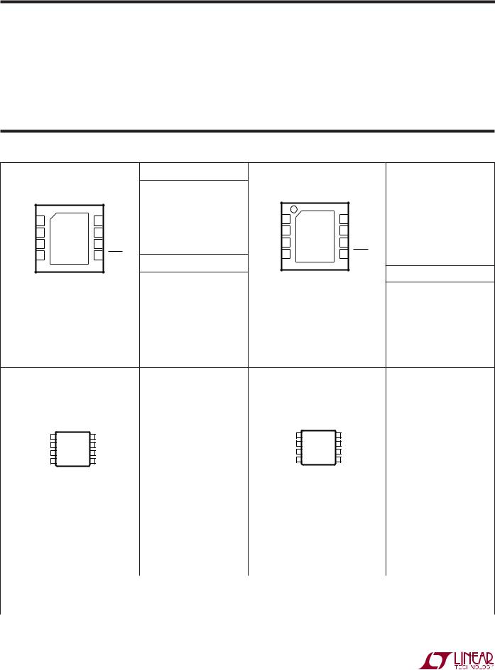
PACKAGE/ORDER IUFORWATIOU
ORDER PART NUMBER |
ORDER PART NUMBER |
|
|
TOP VIEW |
|
LT3020EDD |
|
|
TOP VIEW |
|
LT3020EDD-1.2 |
|
|
|
|
LT3020IDD |
|
|
|
LT3020EDD-1.5 |
|||
|
|
|
|
|
|
|
|
|||
OUT |
1 |
8 |
IN |
|
OUT |
1 |
8 |
IN |
LT3020EDD-1.8 |
|
OUT |
2 |
7 |
IN |
|
OUT |
2 |
7 |
IN |
LT3020IDD-1.2 |
|
|
|
9 |
|
|
OUT |
|
9 |
NC |
LT3020IDD-1.5 |
|
ADJ |
3 |
6 |
NC |
|
3 |
6 |
||||
GND |
4 |
5 |
SHDN |
DD PART MARKING |
GND |
4 |
5 |
SHDN |
LT3020IDD-1.8 |
|
|
|
|
|
|||||||
|
|
|
|
|
|
|
|
DD PART MARKING |
||
|
|
DD PACKAGE |
|
LAEX |
|
|
DD PACKAGE |
|
||
8-LEAD (3mm × 3mm) PLASTIC DFN |
8-LEAD (3mm × 3mm) PLASTIC DFN |
LBKC |
||||||||
TJMAX = 125°C, θJA = 35°C/ W*, θJC = 3°C/ W |
LBYH |
TJMAX = 125°C, θJA = 35°C/ W*, θJC = 3°C/ W |
||||||||
LBKD |
||||||||||
EXPOSED PAD IS GND (PIN 9) CONNECT TO PIN 4 |
|
EXPOSED PAD IS GND (PIN 9) CONNECT TO PIN 4 |
||||||||
*SEE THE APPLICATIONS INFORMATION SECTION |
|
*SEE THE APPLICATIONS INFORMATION SECTION |
LBKF |
|||||||
|
|
|
|
|
||||||
|
|
|
|
|
|
|
|
|
LBYJ |
|
|
|
|
|
|
|
|
|
|
LBYK |
|
|
|
|
|
|
|
|
|
|
LBYM |
|
|
|
|
|
|
ORDER PART NUMBER |
|
|
|
|
|
ORDER PART NUMBER |
|
|
|
|
|
|
LT3020EMS8 |
|
|
|
|
|
LT3020EMS8-1.2 |
|
|
|
|
|
|
LT3020IMS8 |
|
|
|
|
|
LT3020EMS8-1.5 |
|
|
TOP VIEW |
|
|
TOP VIEW |
|
|
|
LT3020EMS8-1.8 |
||||
OUT |
1 |
8 IN |
|
OUT |
1 |
8 IN |
LT3020IMS8-1.2 |
|||||
OUT |
2 |
7 IN |
|
OUT |
2 |
7 IN |
LT3020IMS8-1.5 |
|||||
ADJ |
3 |
6 NC |
|
OUT |
3 |
6 |
NC |
|
||||
|
|
|
|
|
|
|
|
|
|
|
LT3020IMS8-1.8 |
|
GND |
4 |
5 |
|
|
|
GND |
4 |
5 SHDN |
||||
SHDN |
|
|||||||||||
|
|
|
|
|
|
|
||||||
|
MS8 PACKAGE |
|
|
MS8 PACKAGE |
|
|
|
|
||||
|
MS8 PART MARKING |
|
|
|
|
MS8 PART MARKING |
||||||
8-LEAD PLASTIC MSOP |
8-LEAD PLASTIC MSOP |
|||||||||||
TJMAX = 150°C, θJA = 125°C/ W, θJC = 40°C/ W |
|
TJMAX = 150°C, θJA = 125°C/ W, θJC = 40°C/ W |
|
|||||||||
LTAGL |
LTBKG |
|||||||||||
SEE THE APPLICATIONS INFORMATION SECTION |
SEE THE APPLICATIONS INFORMATION SECTION |
|||||||||||
|
|
|
|
|
LTBYN |
|
|
|
|
|
LTBKH |
|
|
|
|
|
|
|
|
|
|
|
|
LTBKJ |
|
|
|
|
|
|
|
|
|
|
|
|
LTBYP |
|
|
|
|
|
|
|
|
|
|
|
|
LTBYQ |
|
|
|
|
|
|
|
|
|
|
|
|
LTBYR |
|
|
|
|
|
|
|
|
|
|||||
Order Options Tape and Reel: Add #TR |
|
|
|
|
|
|
|
|||||
Lead Free: Add #PBF |
Lead Free Tape and Reel: Add #TRPBF |
|
|
|
|
|
|
|||||
Lead Free Part Marking: http://www.linear.com/leadfree/ |
|
|
|
|
|
|
||||||
|
|
|
|
|
|
|
||||||
Consult LTC Marketing for parts specified with wider operating temperature ranges. |
|
|
|
|
|
|
||||||
|
|
|
|
|
|
|
|
|
|
|
3020fc |
|
|
|
|
|
|
|
|
|
|
|
|
|
|
|
|
|
|
|
|
|
|
|
|
|
|
|
2

LT3020/LT3020-1.2/
LT3020-1.5/LT3020-1.8
ELECTRICAL CHARACTERISTICS
The ● denotes specifications which apply over the full operating temperature range, otherwise specifications are TJ = 25°C.
PARAMETER |
CONDITIONS |
|
|
MIN |
TYP |
MAX |
UNITS |
||||||||
|
|
|
|
|
|
|
|
|
|
|
|
|
|
|
|
Minimum Input Voltage (Note 14) |
ILOAD = 100mA, TJ > 0°C |
|
|
0.9 |
1.05 |
V |
|||||||||
|
|
|
ILOAD = 100mA, TJ < 0°C |
|
|
0.9 |
1.10 |
V |
|||||||
ADJ Pin Voltage (Notes 4, 5) |
VIN = 1.5V, ILOAD = 1mA |
|
196 |
200 |
204 |
mV |
|||||||||
|
|
|
1.15V < VIN < 10V, 1mA < ILOAD < 100mA |
● |
193 |
200 |
206 |
mV |
|||||||
Regulated Output Voltage |
LT3020-1.2 |
VIN = 1.5V, ILOAD = 1mA |
|
1.176 |
1.200 |
1.224 |
V |
||||||||
(Note 4) |
|
|
|
|
|
|
|
1.5V < VIN < 10V, 1mA < ILOAD < 100mA |
● |
1.157 |
1.200 |
1.236 |
V |
||
|
|
|
LT3020-1.5 |
VIN = 1.8V, ILOAD = 1mA |
|
1.470 |
1.500 |
1.530 |
V |
||||||
|
|
|
|
|
|
|
|
|
|
1.8V < VIN < 10V, 1mA < ILOAD < 100mA |
● |
1.447 |
1.500 |
1.545 |
V |
|
|
|
LT3020-1.8 |
VIN = 2.1V, ILOAD = 1mA |
|
1.764 |
1.800 |
1.836 |
V |
||||||
|
|
|
|
|
|
|
|
|
|
2.1V < VIN < 10V, 1mA < ILOAD < 100mA |
● |
1.737 |
1.800 |
1.854 |
V |
Line Regulation (Note 6) |
∆VIN = 1.15V to 10V, ILOAD = 1mA |
● |
–1.75 |
0 |
1.75 |
mV |
|||||||||
|
|
|
LT3020-1.2 |
∆VIN = 1.5V to 10V, ILOAD = 1mA |
● |
–10.5 |
0 |
10.5 |
mV |
||||||
|
|
|
LT3020-1.5 |
∆VIN = 1.8V to 10V, ILOAD = 1mA |
● |
–13 |
0 |
13 |
mV |
||||||
|
|
|
LT3020-1.8 |
∆VIN = 2.1V to 10V, ILOAD = 1mA |
● |
–15.8 |
0 |
15.8 |
mV |
||||||
Load Regulation (Note 6) |
VIN = 1.15V, ∆ILOAD = 1mA to 100mA |
|
–1 |
0.4 |
1 |
mV |
|||||||||
|
|
|
LT3020-1.2 |
VIN = 1.5V, ∆ILOAD = 1mA to 100mA |
|
–6 |
1 |
6 |
mV |
||||||
|
|
|
LT3020-1.5 |
VIN = 1.8V, ∆ILOAD = 1mA to 100mA |
|
–7.5 |
1.5 |
7.5 |
mV |
||||||
|
|
|
LT3020-1.8 |
VIN = 2.1V, ∆ILOAD = 1mA to 100mA |
|
–9 |
2 |
9 |
mV |
||||||
Dropout Voltage (Notes 7, 12) |
ILOAD = 10mA |
|
|
|
85 |
115 |
mV |
||||||||
|
|
|
ILOAD = 10mA |
|
● |
|
|
180 |
mV |
||||||
|
|
|
ILOAD = 100mA |
|
|
|
150 |
180 |
mV |
||||||
|
|
|
ILOAD = 100mA |
|
● |
|
|
285 |
mV |
||||||
GND Pin Current |
ILOAD = 0mA |
|
● |
|
120 |
250 |
A |
||||||||
VIN = VOUT(NOMINAL) |
ILOAD = 1mA |
|
|
|
570 |
|
A |
||||||||
(Notes 8, 12) |
ILOAD = 10mA |
|
|
|
920 |
|
A |
||||||||
|
|
|
ILOAD = 100mA |
|
● |
|
2.25 |
3.5 |
mA |
||||||
Output Voltage Noise |
COUT = 2.2 F, ILOAD = 100mA, BW = 10Hz to 100kHz, VOUT = 1.2V |
|
|
245 |
|
VRMS |
|||||||||
ADJ Pin Bias Current |
VADJ = 0.2V, RIPPLE = 1.2V (Notes 6, 9) |
|
|
20 |
50 |
nA |
|||||||||
Shutdown Threshold |
VOUT = Off to On |
|
● |
|
0.61 |
0.9 |
V |
||||||||
|
|
|
VOUT = On to Off |
|
● |
0.25 |
0.61 |
|
V |
||||||
|
|
Pin Current (Note 10) |
V |
|
|
= 0V, VIN = 10V |
|
|
|
±1 |
A |
||||
SHDN |
● |
|
|
||||||||||||
|
SHDN |
|
|
||||||||||||
|
|
|
V |
|
= 10V, VIN = 10V |
● |
|
3 |
9.5 |
A |
|||||
|
|
|
SHDN |
|
|||||||||||
Quiescent Current in Shutdown |
VIN = 6V, V |
|
= 0V |
|
|
3 |
9 |
A |
|||||||
SHDN |
|
|
|||||||||||||
Ripple Rejection (Note 6) |
VIN – VOUT = 1V, VRIPPLE = 0.5VP-P, fRIPPLE = 120Hz, ILOAD = 100mA |
|
|
64 |
|
dB |
|||||||||
|
|
|
LT3020-1.2 VIN – VOUT = 1V, VRIPPLE = 0.5VP-P, fRIPPLE = 120Hz, |
|
|
60 |
|
dB |
|||||||
|
|
|
ILOAD = 100mA |
|
|
|
|
|
|
||||||
|
|
|
LT3020-1.5 VIN – VOUT = 1V, VRIPPLE = 0.5VP-P, fRIPPLE = 120Hz, |
|
|
58 |
|
dB |
|||||||
|
|
|
ILOAD = 100mA |
|
|
|
|
|
|
||||||
|
|
|
LT3020-1.8 VIN – VOUT = 1V, VRIPPLE = 0.5VP-P, fRIPPLE = 120Hz, |
|
|
56 |
|
dB |
|||||||
|
|
|
ILOAD = 100mA |
|
|
|
|
|
|
||||||
3020fc
3

LT3020/LT3020-1.2/
LT3020-1.5/LT3020-1.8
ELECTRICAL CHARACTERISTICS
The ● denotes specifications which apply over the full operating temperature range, otherwise specifications are TJ = 25°C.
PARAMETER |
CONDITIONS |
|
|
MIN |
TYP |
MAX |
UNITS |
Current Limit (Note 12) |
VIN = 10V, VOUT = 0V |
|
|
360 |
|
mA |
|
|
VIN = VOUT(NOMINAL) + 0.5V, ∆VOUT = –5% |
● |
110 |
310 |
|
mA |
|
Input Reverse Leakage Current |
VIN = –10V, VOUT = 0V |
|
|
1 |
10 |
A |
|
Reverse Output Current |
VOUT = 1.2V, VIN = 0V |
|
|
3 |
5 |
A |
|
(Notes 11, 13) |
LT3020-1.2 |
VOUT = 1.2V, VIN = 0V |
|
|
10 |
15 |
A |
|
LT3020-1.5 |
VOUT = 1.5V, VIN = 0V |
|
|
10 |
15 |
A |
|
LT3020-1.8 |
VOUT = 1.8V, VIN = 0V |
|
|
10 |
15 |
A |
Note 1: Absolute Maximum Ratings are those values beyond which the life of a device may be impaired.
Note 2: The LT3020 regulators are tested and specified under pulse load conditions such that TJ ≈ TA. The LT3020E is 100% production tested at TA = 25°C. Performance at –40°C and 125°C is assured by design, characterization and correlation with statistical process controls. The LT3020I is guaranteed over the full –40°C to 125°C operating junction temperature range.
Note 3: This IC includes overtemperature protection that is intended to protect the device during momentary overload conditions. Junction temperature will exceed 125°C when overtemperature protection is active. Continuous operation above the specified maximum operating junction temperature may impair device reliability.
Note 4: Maximum junction temperature limits operating conditions. The regulated output voltage specification does not apply for all possible combinations of input voltage and output current. Limit the output current range if operating at maximum input voltage. Limit the input voltage range if operating at maximum output current.
Note 5: Typically the LT3020 supplies 100mA output current with a 1V input supply. The guaranteed minimum input voltage for 100mA output current is 1.10V.
Note 6: The LT3020 is tested and specified for these conditions with an external resistor divider (20k and 30.1k) setting VOUT to 0.5V. The external resistor divider adds 10 A of output load current. The line regulation and load regulation specifications refer to the change in the 0.2V reference voltage, not the 0.5V output voltage. Specifications for fixed output voltage devices are referred to the output voltage.
Note 7: Dropout voltage is the minimum input to output voltage differential needed to maintain regulation at a specified output current. In dropout the output voltage equals: (VIN – VDROPOUT).
Note 8: GND pin current is tested with VIN = VOUT(NOMINAL) and a current source load. The device is tested while operating in its dropout region.
This condition forces the worst-case GND pin current. GND pin current decreases at higher input voltages.
Note 9: Adjust pin bias current flows out of the ADJ pin.
Note 10: Shutdown pin current flows into the SHDN pin.
Note 11: Reverse output current is tested with IN grounded and OUT forced to the rated output voltage. This current flows into the OUT pin and out of the GND pin. For fixed voltage devices this includes the current in the output resistor divider.
Note 12: The LT3020 is tested and specified for these conditions with an external resistor divider (20k and 100k) setting VOUT to 1.2V. The external resistor divider adds 10 A of load current.
Note 13: Reverse current is higher for the case of (rated_output) < VOUT < VIN, because the no-load recovery circuitry is active in this region and is trying to restore the output voltage to its nominal value.
Note 14: Minimum input voltage is the minimum voltage required by the control circuit to regulate the output voltage and supply the full 100mA rated current. This specification is tested at VOUT = 0.5V. At higher output voltages the minimum input voltage required for regulation will be equal to the regulated output voltage VOUT plus the dropout voltage.
3020fc
4

LT3020/LT3020-1.2/
LT3020-1.5/LT3020-1.8
TYPICAL PERFORWAUCE CHARACTERISTICS
DROPOUT VOLTAGE (mV)
|
Typical Dropout Voltage |
|
|
|
|
|
|
|
|
Dropout Voltage |
|
|
|
|
|
|
|
|
|
|
|
|
|
||||||||||||||||||||||
250 |
|
|
|
|
|
|
|
|
|
|
|
|
|
|
|
|
|
|
|
|
|
|
|
250 |
|
|
|
|
|
|
|
|
|
|
|
|
|
|
|
|
|
|
|
|
|
|
|
|
|
|
|
|
|
|
|
|
|
|
|
|
|
|
|
|
|
|
|
|
|
VOUT = 1.2V |
|
|
|
|
|
|
|
|
|
|
|
|
|
|
|
|
|||||
225 |
|
|
|
|
|
|
|
|
|
|
|
|
|
|
|
|
|
|
|
|
|
|
|
225 |
|
|
|
|
|
|
|
|
|
|
|
|
|
|
|
|
|
||||
|
|
|
|
|
|
|
|
|
|
|
|
|
|
|
|
|
|
|
|
|
|
|
|
|
|
|
|
|
|
|
|
|
|
|
|
|
|
|
|
|
|
||||
|
|
|
|
|
|
|
|
|
|
|
|
|
|
|
|
|
|
|
|
|
|
|
|
|
|
|
|
|
|
|
|
|
|
I |
L = 100mA |
|
|
|
|
||||||
|
|
|
|
|
|
|
|
|
|
|
|
|
|
|
|
|
|
|
|
|
|
|
|
|
|
|
|
|
|
|
|
|
|
|
|
|
|
||||||||
200 |
|
|
|
|
|
|
|
|
|
|
|
|
|
|
|
|
|
|
|
|
|
|
|
200 |
|
|
|
|
|
|
|
|
|
|
|
|
|
|
|
|
|
|
|
|
|
|
|
|
|
|
|
|
TJ = |
125° |
C |
|
|
|
|
|
|
|
|
|
|
(mV) |
|
|
|
|
|
|
|
|
|
|
|
|
|
|
|
|
|
|
|
|
|
||||
|
|
|
|
|
|
|
|
|
|
|
|
|
|
|
|
|
|
|
|
|
|
|
|
|
|
|
|
|
|
|
|
|
|
|
|
|
|||||||||
175 |
|
|
|
|
|
|
|
|
|
|
|
|
|
|
|
|
|
|
|
|
|
|
175 |
|
|
|
|
|
|
|
|
|
|
|
|
|
|
|
|
|
|
|
|
|
|
|
|
|
|
|
|
|
|
|
|
|
|
|
|
|
|
|
|
|
|
|
|
|
|
|
|
|
|
|
|
|
|
|
|
|
|
|
|
|
|
|
|
|
|||
150 |
|
|
|
|
|
|
|
|
|
|
|
|
|
|
|
|
|
|
|
|
|
|
VOLTAGE |
150 |
|
|
|
|
|
|
|
|
|
|
|
|
|
|
|
|
|
|
|
|
|
|
|
|
|
|
|
|
|
|
|
|
|
|
|
|
|
|
|
|
|
|
|
|
|
|
|
|
|
|
|
|
|
|
|
|
|
|
IL = |
50mA |
|
|
|
|
|||
|
|
|
|
|
|
|
|
|
|
|
|
|
|
|
|
|
|
|
|
|
|
|
|
|
|
|
|
|
|
|
|
|
|
|
|
|
|
|
|
||||||
125 |
|
|
|
|
|
|
|
|
|
|
|
|
|
|
|
|
|
|
|
|
|
|
|
125 |
|
|
|
|
|
|
|
|
|
|
|
|
|
|
|
|
|
|
|
|
|
|
|
|
|
|
|
|
|
|
|
|
|
|
|
|
|
|
|
|
|
|
|
|
DROPOUT |
|
|
|
|
|
|
|
|
|
|
|
|
|
|
|
|
IL = |
10mA |
|
|
||
|
|
|
|
|
|
|
|
|
|
|
|
|
° |
|
|
|
|
|
|
|
|
|
|
|
|
|
|
|
|
|
|
|
|
|
|
|
|
||||||||
100 |
|
|
|
|
|
|
|
|
|
|
TJ = 25 C |
|
|
|
|
|
|
|
|
100 |
|
|
|
|
|
|
|
|
|
|
|
|
|
|
|
|
|
|
|
|
|
||||
75 |
|
|
|
|
|
|
|
|
|
|
|
|
|
|
|
|
|
|
|
|
|
|
|
75 |
|
|
|
|
|
|
|
|
|
|
|
|
|
|
|
|
|
|
|
|
|
|
|
|
|
|
|
|
|
|
|
|
|
|
|
|
|
|
|
|
|
|
|
|
|
|
|
|
|
|
|
|
|
|
|
|
|
|
|
|
|
|
|
|
|
||
50 |
|
|
|
|
|
|
|
|
|
|
|
|
|
|
|
|
|
|
|
|
|
|
|
50 |
|
|
|
|
|
|
|
|
|
|
|
|
|
|
|
|
|
|
|
|
|
|
|
|
|
|
|
|
|
|
|
|
|
|
|
|
|
|
|
|
|
|
|
|
|
|
|
|
|
|
|
|
|
|
|
|
|
|
|
IL = |
1mA |
|
|
|
|
||
|
|
|
|
|
|
|
|
|
|
|
|
|
|
|
|
|
|
|
|
|
|
|
|
|
|
|
|
|
|
|
|
|
|
|
|
|
|
|
|
|
|
||||
25 |
|
|
|
|
|
|
|
|
|
|
|
|
|
|
|
|
|
|
|
|
|
|
|
25 |
|
|
|
|
|
|
|
|
|
|
|
|
|
|
|
|
|
|
|
|
|
|
|
|
|
|
|
|
|
|
|
|
|
|
|
|
|
|
|
|
|
|
|
|
|
|
|
|
|
|
|
|
|
|
|
|
|
|
|
|
|
|
|
|
|
||
0 |
|
|
|
|
|
|
|
|
|
|
|
|
|
|
|
|
|
|
|
|
|
|
|
0 |
|
|
|
|
|
|
|
|
|
|
|
|
|
|
|
|
|
|
|
|
|
|
10 |
20 |
30 |
40 |
50 |
60 |
70 |
80 |
90 |
100 |
|
|
|
–25 |
0 |
25 |
50 |
75 |
100 |
125 |
|||||||||||||||||||||||||
0 |
|
–50 |
|||||||||||||||||||||||||||||||||||||||||||
|
|
|
|
|
|
OUTPUT CURRENT (mA) |
|
|
|
|
|
|
|
|
|
|
|
|
|
TEMPERATURE (°C) |
|
|
|
|
|
|
|||||||||||||||||||
|
|
|
|
|
|
|
|
|
|
|
|
|
|
|
|
|
|
|
3020 G01 |
|
|
|
|
|
|
|
|
|
|
|
|
|
|
|
|
|
|
3020 G02 |
|||||||
QUIESCENT CURRENT ( A)
Quiescent Current
250
VIN = 6V 225 VOUT = 1.2V
IL = 0
200
175 |
|
|
|
|
|
|
|
|
|
|
|
|
|
|
|
|
|
|
|
|
|
|
|
|
|
|
|
|
|
|
|
150 |
|
|
|
|
|
|
|
|
|
|
|
|
|
|
|
|
|
|
|
|
|
|
|
|
|
|
|
|
|
|
|
125 |
|
|
|
|
|
|
|
|
|
|
|
|
|
|
|
|
|
|
|
|
|
|
|
|
|
|
|
|
|
|
|
|
|
|
|
V |
|
|
= VIN |
|
|
|
|
||||
100 |
|
|
|
|
SHDN |
|
|
|
|
||||||
|
|
|
|
|
|
|
|
|
|
|
|
|
|
|
|
|
|
|
|
|
|
|
|
|
|
|
|
|
|
|
|
75 |
|
|
|
|
|
|
|
|
|
|
|
|
|
|
|
|
|
|
|
|
|
|
|
|
|
|
|
|
|
|
|
50 |
|
|
|
|
|
|
|
|
|
|
|
|
|
|
|
|
|
|
|
|
|
|
|
|
|
|
|
|
|
|
|
25 |
|
|
|
|
|
|
|
|
|
|
|
|
|
||
|
|
|
|
V |
|
= |
0V |
|
|
|
|||||
|
|
|
|
|
SHDN |
|
|
|
|||||||
0 |
|
|
|
|
|
|
|
|
|
|
|
|
|
|
|
|
–25 |
0 |
25 |
50 |
75 |
|
100 |
125 |
|||||||
–50 |
|
||||||||||||||
TEMPERATURE (°C)
3020 G03
ADJ PIN VOLTAGE (mV)
ADJ Pin Voltage
206
IL = 1mA
204
202
200
198
196
194 –50 –25 0 25 50 75 100 125
TEMPERATURE (°C)
3020 G04
Output Voltage
|
1.830 |
|
|
|
|
|
|
|
|
|
|
|
|
|
|
|
|
IL = 1mA |
|
|
|
|
|
|
|
|
|
|
|
|
|||
|
|
|
|
|
|
|
|
|
|
|
|
|
|
|||
(V) |
1.820 |
|
|
|
|
|
|
|
|
|
|
|
|
|
|
|
|
|
|
|
|
|
|
|
|
|
|
|
|
|
|
||
1.810 |
|
|
|
|
|
|
|
|
|
|
|
|
|
|
|
|
VOLTAGE |
|
|
|
|
|
|
|
|
|
|
|
|
|
|
|
|
1.800 |
|
|
|
|
|
|
|
|
|
|
|
|
|
|
|
|
OUTPUT |
|
|
|
|
|
|
|
|
|
|
|
|
|
|
|
|
1.790 |
|
|
|
|
|
|
|
|
|
|
|
|
|
|
|
|
|
|
|
|
|
|
|
|
|
|
|
|
|
|
|
|
|
|
1.780 |
|
|
|
|
|
|
|
|
|
|
|
|
|
|
|
|
|
|
|
|
|
|
|
|
|
|
|
|
|
|
|
|
|
1.770 |
|
|
|
|
|
|
|
|
|
|
|
|
|
|
|
|
|
–25 |
0 |
25 |
50 |
75 |
100 |
125 |
||||||||
|
–50 |
|||||||||||||||
TEMPERATURE (°C)
3020 G22
Output Voltage
|
1.530 |
|
|
|
|
|
|
|
|
|
|
|
|
|
|
|
|
IL = 1mA |
|
|
|
|
|
|
|
|
|
|
|
|
|||
|
|
|
|
|
|
|
|
|
|
|
|
|
|
|||
(V) |
1.520 |
|
|
|
|
|
|
|
|
|
|
|
|
|
|
|
|
|
|
|
|
|
|
|
|
|
|
|
|
|
|
||
1.510 |
|
|
|
|
|
|
|
|
|
|
|
|
|
|
|
|
VOLTAGE |
|
|
|
|
|
|
|
|
|
|
|
|
|
|
|
|
1.500 |
|
|
|
|
|
|
|
|
|
|
|
|
|
|
|
|
OUTPUT |
|
|
|
|
|
|
|
|
|
|
|
|
|
|
|
|
1.490 |
|
|
|
|
|
|
|
|
|
|
|
|
|
|
|
|
|
|
|
|
|
|
|
|
|
|
|
|
|
|
|
|
|
|
1.480 |
|
|
|
|
|
|
|
|
|
|
|
|
|
|
|
|
|
|
|
|
|
|
|
|
|
|
|
|
|
|
|
|
|
1.470 |
|
|
|
|
|
|
|
|
|
|
|
|
|
|
|
|
|
–25 |
0 |
25 |
50 |
75 |
100 |
125 |
||||||||
|
–50 |
|||||||||||||||
TEMPERATURE (°C)
3020 G23
Output Voltage
|
1.230 |
|
|
|
|
|
|
|
|
|
|
|
|
|
|
|
IL = 1mA |
|
|
|
|
|
|
|
|
|
|
|
|||
|
|
|
|
|
|
|
|
|
|
|
|
|
|||
(V) |
1.220 |
|
|
|
|
|
|
|
|
|
|
|
|
|
|
|
|
|
|
|
|
|
|
|
|
|
|
|
|
||
1.210 |
|
|
|
|
|
|
|
|
|
|
|
|
|
|
|
VOLTAGE |
|
|
|
|
|
|
|
|
|
|
|
|
|
|
|
1.200 |
|
|
|
|
|
|
|
|
|
|
|
|
|
|
|
OUTPUT |
|
|
|
|
|
|
|
|
|
|
|
|
|
|
|
1.190 |
|
|
|
|
|
|
|
|
|
|
|
|
|
|
|
|
|
|
|
|
|
|
|
|
|
|
|
|
|
|
|
|
1.180 |
|
|
|
|
|
|
|
|
|
|
|
|
|
|
|
|
|
|
|
|
|
|
|
|
|
|
|
|
|
|
|
1.170 |
|
|
|
|
|
|
|
|
|
|
|
|
|
|
|
|
–25 |
0 |
25 |
50 |
75 |
100 |
125 |
|||||||
|
–50 |
||||||||||||||
TEMPERATURE (°C)
3020 G24
|
Quiescent Current |
|
|
|
|
|
|
|
|
|
|
GND Pin Current |
|
|
|
|
|
|
|
|
|
|
|
|
|
||||||||||||||||||||||||
|
1000 |
|
|
|
|
|
|
|
|
|
|
|
|
|
|
|
|
|
|
|
|
|
|
|
2500 |
|
|
|
|
|
|
|
|
|
|
|
|
|
|
|
|
|
|
|
|
|
|
|
|
|
|
VOUT = 1.2V |
|
|
|
|
|
|
|
|
|
|
|
|
|
|
|
|
|
|
|
|
|
|
|
|
|
|
|
|
|
|
|
|
|
|
|
|
|
VOUT = 1.2V |
|
||||||||
|
|
|
|
|
|
|
|
|
|
|
|
|
|
|
|
|
|
|
|
|
|
|
|
|
|
|
|
|
|
|
|
|
|
|
|
|
|
|
|
|
|
||||||||
|
900 |
|
IL = 0 |
|
|
|
|
|
|
|
|
|
|
|
|
|
|
|
|
|
|
|
|
2250 |
|
|
|
|
|
|
|
|
|
|
|
|
|
|
|
|
|
|
|
TJ = 25°C |
|
|
|||
|
|
|
|
|
|
|
|
|
|
|
|
|
|
|
|
|
|
|
|
|
|
|
|
|
|
|
|
|
|
|
|
|
|
|
|
|
|
|
|
|
|
|
|||||||
CURRENTQUIESCENT( A) |
800 |
|
TJ = 25°C |
|
|
|
|
|
|
|
|
|
|
|
|
|
|
|
|
|
|
2000 |
|
|
|
|
|
|
|
|
|
|
|
|
|
|
|
|
|
|
|
|
|
|
|
|
|||
|
|
|
|
|
|
|
|
|
|
|
|
|
|
|
|
|
|
|
|
|
|
|
|
|
|
|
|
|
|
|
|
|
|
|
|
|
|
|
|
|
|
|
|||||||
|
|
|
|
|
|
|
|
|
|
|
|
|
|
|
|
|
|
|
|
|
|
|
|
|
|
|
|
|
|
|
|
|
|
|
|
|
|
|
|
|
|
|
|
|
|
|
|||
|
|
|
|
|
|
|
|
|
|
|
|
|
|
|
|
|
|
|
|
|
|
|
|
|
|
|
|
|
|
|
|
|
|
|
|
|
|
|
|
|
|
|
|
|
|
||||
700 |
|
|
|
|
|
|
|
|
|
|
|
|
|
|
|
|
|
|
|
|
|
|
|
1750 |
|
|
|
|
|
|
|
RL |
= 12 |
Ω |
|
|
|
|
|
|
|
|
|
|
|
||||
|
|
|
|
|
|
|
|
|
|
|
|
|
|
|
|
|
|
|
|
|
|
|
|
|
|
|
|
|
|
IL = 100mA |
|
|
|
|
|
|
|
|
|
|
|
||||||||
|
|
|
|
|
|
|
|
|
|
|
|
|
|
|
|
|
|
|
|
|
|
|
|
CURRENTPINGNDA)( |
|
|
|
|
|
|
|
|
|
|
|
|
|
|
|
|
|
|
|||||||
|
600 |
|
|
|
|
|
|
|
|
|
|
|
|
|
|
|
|
|
|
|
|
|
|
|
1500 |
|
|
|
|
|
|
|
|
|
|
|
|
|
|
|
|
|
|
|
|
|
|
|
|
|
|
|
|
|
|
|
|
|
|
|
|
|
|
|
|
|
|
|
|
|
|
|
|
|
|
|
|
|
|
|
|
|
|
|
|
|
|
|
|
|
|
|
|
|
|
|
|
||
|
500 |
|
|
|
|
|
|
|
|
|
|
|
|
|
|
|
|
|
|
|
|
|
|
|
1250 |
|
|
|
|
|
|
|
|
|
|
|
|
|
|
|
|
|
|
|
|
|
|
|
|
|
|
|
|
|
|
|
|
|
|
|
|
|
|
|
|
|
|
|
|
|
|
|
|
|
|
|
|
|
RL = 24Ω |
|
|
|
|
|
|
|
|
|
|
|
|
|
|
||||||
|
|
|
|
|
|
|
|
|
|
|
|
|
|
|
|
|
|
|
|
|
|
|
|
|
|
|
|
|
|
|
|
|
|
|
|
|
|
|
|
|
|
|
|
|
|||||
|
400 |
|
|
|
|
|
|
|
|
|
|
|
|
|
|
|
|
|
|
|
|
|
|
|
1000 |
|
|
|
|
|
IL = 50mA |
|
|
|
|
|
|
|
|
|
|
|
|
|
|
||||
|
|
|
|
|
|
|
|
|
|
|
|
|
|
|
|
|
|
|
|
|
|
|
|
|
|
|
|
|
|
|
|
|
|
|
|
|
|
|
|
|
|
|
|||||||
|
300 |
|
|
|
|
|
|
|
|
|
|
|
|
|
|
|
|
|
|
|
|
|
|
|
750 |
|
|
|
|
|
|
|
|
|
|
|
|
|
|
|
|
|
|
|
|
|
|
||
|
|
|
|
|
|
|
|
|
|
|
|
|
|
|
|
|
|
|
|
|
|
|
|
|
|
|
|
RL = |
120 |
Ω |
|
|
|
|
|
|
|
|
|
|
|
|
|
|
|||||
|
200 |
|
|
|
|
|
|
|
|
|
|
|
|
|
|
|
|
|
|
|
|
|
|
|
500 |
|
|
|
|
IL = |
10mA |
|
|
|
|
|
|
|
|
|
|
|
|
|
|
|
|||
|
|
|
|
|
|
|
|
|
|
|
|
|
|
|
|
|
|
|
|
|
|
|
|
|
|
|
|
|
|
|
|
|
|
|
|
|
|
|
|||||||||||
|
|
|
|
|
|
|
|
|
|
|
|
|
|
|
|
|
|
|
|
|
|
|
|
|
|
|
|
|
|
|
|
|
|
|
|
|
|
|
|
|
|
||||||||
|
|
|
|
|
|
|
|
|
VSHDN = VIN |
|
|
|
|
|
|
|
|
|
|
|
|
|
|
|
|
|
|
|
|
|
|
||||||||||||||||||
|
|
|
|
|
|
|
|
|
|
|
|
|
|
|
|
|
|
|
|
|
|
|
|
|
|
|
|
|
|
|
|
|
|
|
|
|
|
|
|
|
|
||||||||
|
100 |
|
|
|
|
|
|
|
|
|
|
|
|
|
|
|
|
|
|
|
|
|
|
|
250 |
|
|
|
R |
L = 1.2k, IL = 1mA |
|
|
|
|
|
|
|
|
|
|
|
||||||||
|
|
|
|
|
|
|
|
|
|
|
|
|
|
|
|
|
|
|
|
|
|
|
|
|
|
|
|
|
|
|
|
|
|
|
|
|
|
||||||||||||
|
|
|
|
|
|
|
|
|
V |
|
|
= 0V |
|
|
|
|
|
|
|
|
|
|
|
|
|
|
|
|
|
|
|
|
|
|
|||||||||||||||
|
0 |
|
|
|
|
|
|
|
|
SHDN |
|
|
|
|
|
|
|
|
0 |
|
|
|
|
|
|
|
|
|
|
|
|
|
|
|
|
|
|
|
|
|
|
|
|
||||||
|
|
|
|
|
|
|
|
|
|
|
|
|
|
|
|
|
|
|
|
|
|
|
|
|
|
|
|
|
|
|
|
|
|
|
|
|
|
|
|
|
|
|
|
|
|
|
|
||
|
|
1 |
2 |
3 |
|
4 |
5 |
|
|
6 |
|
7 |
8 |
9 |
10 |
|
1 |
2 |
3 |
4 |
|
|
5 |
6 |
7 |
|
8 |
9 |
10 |
||||||||||||||||||||
|
0 |
|
|
|
|
0 |
|
|
|
||||||||||||||||||||||||||||||||||||||||
|
|
|
|
|
|
|
INPUT VOLTAGE (V) |
|
|
|
|
|
|
|
|
|
|
|
INPUT VOLTAGE (V) |
|
|
|
|
|
|||||||||||||||||||||||||
|
|
|
|
|
|
|
|
|
|
|
|
|
|
|
|
|
|
|
|
|
3020 G05 |
|
|
|
|
|
|
|
|
|
|
|
|
|
|
|
|
|
|
|
|
|
3020 G06 |
||||||
3020fc
5
 Loading...