


LTC1149
LTC1149-3.3/LTC1149-5
High Efficiency Synchronous
Step-Down Switching Regulators
FEATURES
■Operation to 48V Input Voltage
■Ultrahigh Efficiency: Up to 95%
■Current Mode Operation for Excellent Line and Load Transient Response
■High Efficiency Maintained over Wide Current Range
■Logic-Controlled Micropower Shutdown
■Short-Circuit Protection
■Very Low Dropout Operation: 100% Duty Cycle
■Synchronous FET Switching for High Efficiency
■Adaptive Nonoverlap Gate Drives
■Available in 16-Pin Narrow SO Package
APPLICATIOUS
■Notebook and Palmtop Computers
■Portable Instruments
■Battery-Operated Digital Devices
■Industrial Power Distribution
■Avionics Systems
■Telecom Power Supplies
, LTC and LT are registered trademarks of Linear Technology Corporation.
Burst Mode is a trademark of Linear Technology Corporation.
DESCRIPTIOU
The LTC®1149 series is a family of synchronous stepdown switching regulator controllers featuring automatic Burst ModeTM operation to maintain high efficiencies at low output currents. These devices drive external complementary power MOSFETs at switching frequencies up to 250kHz using a constant off-time current-mode architecture.
Special onboard regulation and level-shift circuitry allow operation at input voltages from dropout to 48V (60V absolute max). The constant off-time architecture maintains constant ripple current in the inductor, easing the design of wide input range converters. Current mode operation provides excellent line and load transient response. The operating current level is user-program- mable via an external current sense resistor.
The LTC1149 series incorporates automatic power saving Burst Mode operation when load currents drop below the level required for continuous operation. Standby power is reduced to only about 8mW at VIN = 12V. In shutdown, both MOSFETs are turned off.
TYPICAL APPLICATIOU
|
|
|
|
|
VIN |
|
|
|
|
|
|
|
|
|
|
|
+ |
CIN |
|
|
|
LTC1149-5 Efficiency |
|
|
1N4148 |
|
|
1N4148 |
|
|
100 |
|
|
||
|
|
VIN |
|
100μF |
|
|
|
|
|||
|
|
|
|
|
|
|
|
||||
|
|
CAP |
PGATE |
|
P-CHANNEL |
100V |
|
|
FIGURE 1 CIRCUIT |
|
|
|
0.068μF |
|
|
IRFR9024 |
|
|
|
|
VIN = 12V |
|
|
|
|
|
|
|
|
|
|
|
|
||
+ |
|
VCC |
PDRIVE |
0.047μF |
|
|
|
|
90 |
|
|
3.3μF |
|
VCC |
D1 |
L* |
RSENSE** |
|
|
|
|
|
|
|
|
|
(%) |
|
|
|
|||||
|
|
LTC1149-5 |
1N5819 |
62μH |
0.05Ω |
VOUT |
|
VIN = 24V |
|
||
>2V = SHUTDOWN |
1000pF |
|
|
EFFICIENCY |
|
|
|||||
SHDN2 |
|
|
|
5V/2A |
80 |
|
|
||||
|
|
|
|
|
|
|
|
|
|
||
|
|
|
SENSE+ |
|
|
|
|
|
|
|
|
0V = NORMAL |
SHDN1 |
|
|
|
|
|
|
|
|
||
|
|
|
|
|
|
|
|
|
|
||
|
|
ITH |
SENSE– |
|
|
+ |
|
|
70 |
|
|
3300μF |
|
NGATE |
|
N-CHANNEL |
COUT |
|
|
|
|||
|
CT |
|
|
|
|
|
|
||||
|
CT |
|
IRFR024 |
|
220μF |
|
|
|
|
||
1k |
SGND |
P, RGNDS |
|
|
|
|
|
|
|
|
|
470pF |
|
|
|
|
|
|
|
60 |
|
|
|
|
|
|
|
|
|
|
|
|
|
||
|
|
|
|
|
|
|
|
|
0.2 |
2 |
|
|
|
|
|
|
*COILTRONICS CTX62-2-MP |
|
|
0.02 |
|||
|
|
|
|
|
**KRL SL-1-C1-0R050J |
1149 F01 |
|
|
LOAD CURRENT (A) |
|
|
|
|
|
|
|
|
|
|
|
|
|
|
|
|
|
|
|
|
|
|
|
|
|
1149 TA01 |
Figure 1. High Efficiency Step-Down Regulator
1
LTC1149 |
|
LTC1149-3.3/LTC1149-5 |
|
ABSOLUTE WAXIWUW |
RATIUGS |
Input Supply Voltage (Pin 2)...................... |
|
– 15V to 60V |
VCC Output Current (Pin 3) .................................. |
|
50mA |
VCC Input Voltage (Pin 5)........................................ |
|
16V |
Continuous Output Current (Pins 4, 13) |
.............. 50mA |
|
Sense Voltages (Pins 8, 9) |
|
|
VIN ³ 12.7V .......................................... |
|
13V to – 0.3V |
VIN < 12.7V ............................. |
(VCC + 0.3V) to – 0.3V |
|
Shutdown Voltages (Pins 10, 15) ............................. |
|
7V |
Operating Temperature Range .................... |
|
0 ° C to 70°C |
Extended Commercial |
|
– 40 ° C to 85°C |
Temperature Range ............................... |
|
|
Junction Temperature (Note 1) ............................ |
|
125°C |
Storage Temperature Range ................ |
|
– 65 ° C to 150°C |
Lead Temperature (Soldering, 10 sec)................. |
300°C |
|
PACKAGE/ORDER IUFORWATIOU
|
|
|
TOP VIEW |
|
|
|
ORDER PART |
PGATE |
|
1 |
|
|
16 |
CAP |
NUMBER |
|
|
|
|
|
|
SHDN2 |
|
VIN |
|
2 |
|
|
15 |
LTC1149CN |
|
|
|
|
|
|
RGND |
||
VCC |
|
3 |
|
|
14 |
||
|
|
|
|
|
|
||
PDRIVE |
|
4 |
|
|
13 |
NGATE |
LTC1149CN-3.3 |
|
|
|
|
|
|
|
|
VCC |
|
5 |
|
|
12 |
PGND |
LTC1149CN-5 |
|
|
|
|
|
|
||
CT |
|
6 |
|
|
11 |
SGND |
LTC1149CS |
|
|
|
|
|
|
VFB / |
|
ITH |
|
7 |
|
|
10 |
LTC1149CS-3.3 |
|
|
|
|
SHDN1* |
||||
|
|
|
|
|
|||
SENSE– |
|
8 |
|
|
9 |
SENSE+ |
LTC1149CS-5 |
|
|
|
|
|
|
|
|
N PACKAGE |
S PACKAGE |
|
|||||
16-LEAD PDIP 16-LEAD PLASTIC SO |
|
||||||
|
*FIXED OUTPUT VERSIONS |
|
|||||
TJMAX = 125°C, θJA = 70°C/ W (N)
TJMAX = 125°C, θJA = 110°C/ W (S)
Consult factory for Industrial and Military grade parts.
ELECTRICAL CHARACTERISTICS TA = 25°C, VIN = 12V, V10 = 0V (Note 2), unless otherwise noted.
SYMBOL |
PARAMETER |
CONDITIONS |
|
MIN |
TYP |
MAX |
UNITS |
|
|
|
|
|
|
|
|
|
|
V10 |
Feedback Voltage (LTC1149 Only) |
VIN = 9V |
● |
1.21 |
1.25 |
1.29 |
V |
|
I10 |
Feedback Current (LTC1149 Only) |
|
● |
|
0.2 |
1 |
μA |
|
VOUT |
Regulated Output Voltage |
VIN = 9V |
|
|
|
|
|
|
|
LTC1149-3.3 |
ILOAD = 700mA |
● |
3.23 |
3.33 |
3.43 |
V |
|
|
LTC1149-5 |
ILOAD = 700mA |
● |
4.9 |
5.05 |
5.2 |
V |
|
VOUT |
Output Voltage Line Regulation |
VIN = 9V to 48V, ILOAD = 50mA |
|
– 40 |
0 |
40 |
mV |
|
|
Output Voltage Load Regulation |
|
|
|
|
|
|
|
|
LTC1149-3.3 |
5mA < ILOAD < 2A |
● |
|
40 |
65 |
mV |
|
|
LTC1149-5 |
5mA < ILOAD < 2A |
● |
|
60 |
100 |
mV |
|
|
Burst Mode Output Ripple |
ILOAD = 0A |
|
|
50 |
|
mVP-P |
|
I2 |
Input DC Supply Current (Note 3) |
|
|
|
|
|
|
|
|
Normal Mode |
VIN = 12V |
|
|
2.0 |
2.8 |
mA |
|
|
|
|
VIN = 48V |
|
|
2.2 |
3.0 |
mA |
|
Burst Mode |
VIN = 12V |
|
|
0.6 |
0.9 |
mA |
|
|
|
|
VIN = 48V |
|
|
0.8 |
1.1 |
mA |
|
Shutdown |
VIN = 12V, V15 = 2V |
|
|
135 |
170 |
μA |
|
|
|
|
VIN = 48V, V15 = 2V |
|
|
300 |
390 |
μA |
VCC |
Internal Regulator Voltage |
VIN = 12V to 48V |
● |
9.75 |
10.25 |
11 |
V |
|
|
(Sets MOSFET Gate Drive Levels) |
I3 = 20mA |
|
|
|
|
|
|
V2 – V3 |
VCC Dropout Voltage |
VIN = 5V, I3 = 10mA |
|
|
200 |
250 |
mV |
|
VIN – V1 |
P-Gate to Source Voltage (Off) |
VIN = 12V |
● |
– 0.2 |
0 |
|
V |
|
|
|
|
VIN = 48V |
● |
– 0.2 |
0 |
|
V |
2

LTC1149
LTC1149-3.3/LTC1149-5
ELECTRICAL CHARACTERISTICS TA = 25°C, VIN = 12V, V10 = 0V (Note 2), unless otherwise noted.
SYMBOL |
PARAMETER |
CONDITIONS |
|
|
|
MIN |
TYP |
MAX |
UNITS |
|||||
|
|
|
|
|
|
|
|
|
|
|
|
|||
V9 – V8 |
Current Sense Threshold Voltage |
|
|
|
|
|
|
|
|
|
|
|||
|
|
LTC1149 |
V8 = 5V, V10 = 1.32V (Forced) |
|
|
|
25 |
|
mV |
|||||
|
|
|
|
|
V8 = VOUT – 100mV |
|
|
● |
130 |
150 |
170 |
mV |
||
|
|
LTC1149-3.3 |
V8 = 3.5V (Forced) |
|
|
|
|
25 |
|
mV |
||||
|
|
|
|
|
V8 = VOUT – 100mV |
|
|
● |
130 |
150 |
170 |
mV |
||
|
|
LTC1149-5 |
V8 = 5.3V (Forced) |
|
|
|
|
25 |
|
mV |
||||
|
|
|
|
|
V8 = VOUT – 100mV |
|
|
● |
130 |
150 |
170 |
mV |
||
V10 |
Shutdown 1 Threshold |
|
|
|
|
|
|
0.5 |
0.8 |
2 |
V |
|||
|
|
LTC1149-3.3, LTC1149-5 |
|
|
|
|
|
|
||||||
V15 |
Shutdown 2 Threshold |
|
|
|
|
|
|
0.8 |
1.4 |
2 |
V |
|||
I15 |
Shutdown 2 Input Current |
V15 = 5V |
|
|
|
|
18 |
25 |
μA |
|||||
I |
6 |
C |
T |
Pin Discharge Current |
V |
OUT |
In Regulation, V |
– = V |
OUT |
|
50 |
70 |
90 |
μA |
|
|
|
|
|
SENSE |
|
|
|
|
μA |
||||
|
|
|
|
|
VOUT = 0V |
|
|
|
|
2 |
10 |
|||
tOFF |
Off-Time (Note 4) |
CT = 390pF, ILOAD = 700mA |
|
|
4 |
5 |
6 |
μs |
||||||
tr, tf |
Driver Output Transition Times |
CL = 3000pF (Pins 4, 13), VIN = 6V |
|
|
100 |
200 |
ns |
|||||||
– 40°C ≤ TA ≤ 85°C (Note 5), unless otherwise noted.
SYMBOL |
PARAMETER |
CONDITIONS |
MIN |
TYP |
MAX |
UNITS |
|
|
|
|
|
|
|
|
|
V10 |
Feedback Voltage LTC1149 Only |
|
|
1.2 |
1.25 |
1.3 |
V |
VOUT |
Regulated Output Voltage |
VIN = 9V |
|
|
|
|
|
|
LTC1149-3.3 |
ILOAD = 700mA |
|
3.17 |
3.33 |
3.43 |
V |
|
LTC1149-5 |
ILOAD = 700mA |
|
4.85 |
5.05 |
5.2 |
V |
I2 |
Input DC Supply Current (Note 3) |
|
|
|
|
|
|
|
Normal Mode |
VIN = 12V |
|
|
2.0 |
3.2 |
mA |
|
|
VIN = 48V |
|
|
2.2 |
3.5 |
mA |
|
Burst Mode |
VIN = 12V |
|
|
0.6 |
1.05 |
mA |
|
|
VIN = 48V |
|
|
0.8 |
1.30 |
mA |
|
Shutdown |
VIN = 12V, V15 = 2V |
|
|
135 |
230 |
μA |
|
|
VIN = 48V, V15 = 2V |
|
|
300 |
520 |
μA |
VCC |
Internal Regulator Voltage |
VIN = 12V to 48V |
|
9.75 |
10.25 |
11 |
V |
|
(Sets MOSFET Gate Drive Levels) |
I3 = 20mA |
|
|
|
|
|
V9 – V8 |
Current Sense Threshold Voltage |
Low Threshold (Forced) |
|
125 |
25 |
175 |
mV |
|
|
High Threshold (Forced) |
|
150 |
mV |
||
V15 |
Shutdown 2 Threshold |
|
|
0.8 |
1.4 |
2 |
V |
tOFF |
Off-Time (Note 4) |
CT = 390pF, ILOAD = 700mA, VIN = 10V |
|
3.8 |
5 |
6 |
μs |
The ● denotes specifications which apply over the full operating temperature range.
Note 1: TJ is calculated from the ambient temperature TA and power dissipation PD according to the following formulas:
LTC1149CN, LTC1149CN-3.3, LTC1149CN-5: TJ = TA + (PD )(70°C/W) LTC1149CS, LTC1149CS-3.3, LTC1149CS-5: TJ = TA + (PD)(110°C/W)
Note 2: Pin 10 is a shutdown pin on the LTC1149-3.3 and LTC1149-5 fixed output voltage versions and must be at ground potential for testing.
Note 3: Dynamic supply current is higher due to the gate charge being delivered at the switching frequency. The allowable operating frequency may be limited by power dissipation at high input voltages. See Typical Performance Characteristics and Applications Information.
Note 4: In applications where RSENSE is placed at ground potential, the offtime increases approximately 40%.
Note 5: The LTC1149, LTC1149-3.3, and LTC1149-5 are not tested and not quality assurance sampled at – 40°C and 85°C. These specifications are guaranteed by design and/or correlation.
3
LTC1149
LTC1149-3.3/LTC1149-5
TYPICAL PERFORWAUCE CHARACTERISTICS
Efficiency vs Input Voltage
|
100 |
|
|
|
|
|
|
|
|
FIGURE |
1 CIRCUIT |
|
|
|
|
|
|
ILOAD |
= 1A |
|
|
|
|
(%) |
95 |
|
|
|
|
|
|
|
|
|
|
|
|
||
|
|
|
|
|
|
|
|
EFFICIENCY |
90 |
|
|
|
|
|
|
|
|
|
|
|
|
|
|
|
85 |
|
|
|
|
|
|
|
|
|
|
|
|
|
|
|
80 |
|
|
|
|
|
|
|
|
|
|
|
|
|
|
0 10 20 30 40 50 INPUT VOLTAGE (V)
1149 G01
DC Supply Current
|
3.0 |
|
|
|
|
|
|
|
|
|
|
|
|
|
|
(mA) |
2.5 |
|
|
|
|
|
|
|
|
ACTIVE |
|
MODE |
|
||
|
|
|
|
|
|||
|
|
|
|
|
|||
|
|
|
|
|
|
||
CURRENT |
2.0 |
|
|
|
|
|
|
|
|
|
|
|
|
||
1.5 |
|
|
|
|
|
|
|
SUPPLY |
|
|
|
|
|
|
|
1.0 |
|
|
|
|
|
|
|
|
|
|
SLEEP |
|
MODE |
|
|
|
|
|
|
|
|
||
|
0.5 |
|
|
|
|
|
|
|
|
|
|
|
|
|
|
|
0 |
|
|
|
|
|
|
|
|
|
|
|
|
|
0 10 20 30 40 50 INPUT VOLTAGE (V)
1149 G04
Gate Charge Supply Current
|
30 |
|
|
|
|
|
|
|
|
|
|
|
|
|
|
|
|
|
|
|
|
|
|
(mA) |
25 |
|
|
|
|
|
|
|
|
|
|
|
|
|
|
|
|
|
|
|
|
||
|
|
|
|
|
|
|
|
|
|
|
|
CURRENT |
20 |
|
|
|
|
|
|
|
|
|
|
|
|
|
|
|
|
|
|
|
|
|
|
|
|
|
Q |
P + QN = 100nC |
|
|
|
|
|
||
CHARGE |
15 |
|
|
|
|
|
|
|
|
|
|
|
|
|
|
|
|
|
|
|
|
||
10 |
|
|
|
|
|
|
|
|
|
|
|
|
|
|
|
|
|
|
|
|
|
||
GATE |
|
|
|
|
|
|
|
|
|
|
|
5 |
|
|
|
|
Q |
P + QN = 50nC |
|
|
|||
|
|
|
|
|
|
|
|
|
|
|
|
|
|
|
|
|
|
|
|
|
|
|
|
|
0 |
|
|
|
|
|
|
|
|
|
|
|
|
100 |
150 |
200 |
|
250 |
|||||
|
50 |
|
|||||||||
OPERATING FREQUENCY (kHz)
1149 G07
Line Regulation |
Load Regulation |
|
60 |
FIGURE 1 CIRCUIT |
|
|
|
|
20 |
|
|
FIGURE 1 CIRCUIT |
|||
|
|
|
|
|
|
|
|
|
|||||
|
40 |
ILOAD = 1A |
|
|
|
|
|
0 |
|
|
VIN = 24V |
|
|
|
|
|
|
|
|
|
|
|
|
|
|
||
(mV) |
20 |
|
|
|
|
|
(mV) |
–20 |
|
|
|
|
|
0 |
|
|
|
|
|
–40 |
|
|
|
|
|
||
OUT |
|
|
|
|
|
OUT |
|
|
|
|
|
||
|
|
|
|
|
|
|
|
|
|
|
|
||
V |
|
|
|
|
|
|
V |
|
|
|
|
|
|
|
–20 |
|
|
|
|
|
|
–60 |
|
|
|
|
|
|
–40 |
|
|
|
|
|
|
–80 |
|
|
|
|
|
|
–60 |
10 |
20 |
30 |
40 |
50 |
–100 |
0.5 |
1.0 |
1.5 |
2.0 |
2.5 |
|
|
0 |
|
0 |
||||||||||
|
|
|
INPUT VOLTAGE (V) |
|
|
|
|
|
LOAD CURRENT (A) |
|
|
||
|
|
|
|
|
|
1149 G02 |
|
|
|
|
|
|
1149 G03 |
|
|
|
|
|
|
|
|
|
|
|
|
|
|
|
|
|
|
|
|
|
|
|
|
Operating Frequency |
|
|
|
|
|
|
|
|||||||||||
|
Supply Current in Shutdown |
|
|
|
|
|
|
vs (VIN – VOUT) |
|
|
|
|
|
|
|
|
|
|
|
|||||||||||||||||||||||
|
400 |
|
|
|
|
|
|
|
|
|
|
|
|
|
|
|
|
|
|
|
|
|
2.0 |
|
|
|
|
|
|
|
|
|
|
|
|
|
|
|
|
|
|
|
|
|
|
VSD2 = |
|
2V |
|
|
|
|
|
|
|
|
|
|
|
|
|
|
|
|
|
|
|
|
|
|
|
|
|
|
|
|
|
|
|
|
|
|
|||
|
|
|
|
|
|
|
|
|
|
|
|
|
|
|
|
|
|
|
|
|
|
|
VOUT = |
5V |
|
|
|
|
|
|
|
|
|
|
|
|
|
|
||||
|
|
|
|
|
|
|
|
|
|
|
|
|
|
|
|
|
|
|
|
|
|
|
|
|
|
|
|
|
|
|
|
|
|
|
|
|
|
|
|
|
||
|
|
|
|
|
|
|
|
|
|
|
|
|
|
|
|
|
|
|
|
|
|
|
|
|
|
|
|
|
|
|
|
T = 0°C |
|
|
|
|
|
|
|
|||
A)(CURRENTSUPPLYμ |
100 |
|
|
|
|
|
|
|
|
|
|
|
|
|
|
|
|
|
|
|
|
FREQUENCYNORMALIZED |
0.5 |
|
|
|
|
|
|
|
|
|
|
|
|
|
|
|
|
|
|
|
|
300 |
|
|
|
|
|
|
|
|
|
|
|
|
|
|
|
|
|
|
|
|
|
1.5 |
|
|
|
|
|
|
|
|
|
|
|
|
|
|
|
|
|
|
|
|
|
|
|
|
|
|
|
|
|
|
|
|
|
|
|
|
|
|
|
|
|
|
|
|
|
|
|
|
|
|
|
|
|
T = 25 |
|
°C |
|
|
|
|||
|
|
|
|
|
|
|
|
|
|
|
|
|
|
|
|
|
|
|
|
|
|
|
|
|
|
|
|
|
|
|
|
|
|
|
|
|
|
|
|
|||
|
200 |
|
|
|
|
|
|
|
|
|
|
|
|
|
|
|
|
|
|
|
|
|
1.0 |
|
|
|
|
|
|
|
|
T = 70°C |
|
|
|
|||||||
|
|
|
|
|
|
|
|
|
|
|
|
|
|
|
|
|
|
|
|
|
|
|
|
|
|
|
|
|
|
|
|
|
|
|
|
|
||||||
|
|
|
|
|
|
|
|
|
|
|
|
|
|
|
|
|
|
|
|
|
|
|
|
|
|
|
|
|
|
|
|
|
|
|
|
|
|
|
|
|
||
|
|
|
|
|
|
|
|
|
|
|
|
|
|
|
|
|
|
|
|
|
|
|
|
|
|
|
|
|
|
|
|
|
|
|
|
|
|
|
|
|
||
|
0 |
|
|
|
|
|
|
|
|
|
|
|
|
|
|
|
|
|
|
|
|
|
0 |
|
|
|
|
|
|
|
|
|
|
|
|
|
|
|
|
|
|
|
|
|
|
|
|
|
|
|
|
|
|
|
|
|
|
|
|
|
|
|
|
|
|
|
|
|
|
|
|
|
|
|
|
|
|
|
|
|
|
|
|
||
|
|
|
10 |
20 |
|
30 |
|
|
40 |
50 |
|
|
|
5 |
10 |
15 |
20 |
25 |
||||||||||||||||||||||||
|
0 |
|
|
|
|
0 |
||||||||||||||||||||||||||||||||||||
|
|
|
|
|
|
|
|
INPUT VOLTAGE (V) |
|
|
|
|
|
|
|
|
|
|
|
|
(VIN – VOUT) VOLTAGE (V) |
|
|
|
||||||||||||||||||
|
|
|
|
|
|
|
|
|
|
|
|
|
|
|
|
|
|
1149 G05 |
|
|
|
|
|
|
|
|
|
|
|
|
|
|
|
|
|
|
1149 G06 |
|||||
|
Off-Time vs VOUT |
|
|
|
|
|
|
|
|
|
|
|
|
Current Sense Threshold Voltage |
||||||||||||||||||||||||||||
|
80 |
|
|
|
|
|
|
|
|
|
|
|
|
|
|
|
|
|
|
|
|
|
160 |
|
|
|
|
|
|
|
|
|
|
|
|
|
|
|
|
|
|
|
|
|
|
|
|
|
|
|
|
|
|
|
|
|
|
|
|
|
|
|
|
|
|
|
|
|
|
|
|
|
|
|
|
|
|
|
|
|
|
||||
|
70 |
|
|
|
|
|
|
|
|
|
|
|
|
|
|
|
|
|
|
|
|
|
140 |
|
|
|
|
|
|
|
|
|
|
|
|
|
|
|
|
|
|
|
|
|
|
|
|
|
|
|
|
|
|
|
|
|
|
|
|
|
|
|
|
|
|
|
|
|
|
|
|
|
|
|
|
|
|
|
|
|
|
|
|||
|
|
|
|
|
|
|
|
|
|
|
|
|
|
|
|
|
|
|
|
|
|
|
|
|
|
|
|
|
|
|
MAXIMUM |
|
|
|
||||||||
s)(TIME-OFFμ |
60 |
|
|
|
|
|
|
|
|
|
|
|
|
|
|
|
|
|
|
|
|
VOLTAGESENSE(mV) |
120 |
|
|
|
|
|
|
|
|
|
|
THRESHOLD |
|
|
|
|||||
|
|
|
|
|
|
|
|
|
|
|
|
|
|
|
|
|
|
|
|
|
|
|
|
|
|
|
|
|
|
|
|
|
||||||||||
|
|
|
|
|
|
|
|
|
|
|
|
|
|
|
|
|
|
|
|
|
|
|
|
|
|
|
|
|
|
|
|
|
|
|
|
|
|
|
||||
|
|
|
|
|
|
|
|
|
|
|
|
|
|
|
|
|
|
|
|
|
|
|
|
|
|
|
|
|
|
|
|
|
|
|
|
|
||||||
50 |
|
|
|
|
|
|
|
|
|
|
|
|
|
|
|
|
|
|
|
|
100 |
|
|
|
|
|
|
|
|
|
|
|
|
|
|
|
|
|
|
|
||
|
|
|
|
|
|
|
|
|
|
|
|
|
|
|
|
|
|
|
|
|
|
|
|
|
|
|
|
|
|
|
|
|
|
|
|
|
|
|
||||
|
|
|
|
|
|
|
|
|
|
|
|
|
|
|
|
|
|
|
|
|
|
|
|
|
|
|
|
|
|
|
|
|
|
|
|
|
|
|
|
|
||
|
40 |
|
|
|
|
|
|
|
|
|
|
|
|
|
|
|
|
|
|
|
|
|
80 |
|
|
|
|
|
|
|
|
|
|
|
|
|
|
|
|
|
|
|
|
|
|
|
|
|
|
|
|
|
|
|
|
|
|
|
|
|
|
|
|
|
|
|
|
|
|
|
|
|
|
|
|
|
|
|
|
|
|
|
|
||
|
|
|
|
|
|
|
|
|
|
|
|
|
|
|
|
|
|
|
|
|
|
|
|
|
|
|
|
|
|
|
|
|
|
|
|
|
|
|
||||
|
30 |
|
|
|
|
|
|
|
|
|
|
|
|
|
|
|
|
|
|
|
|
|
60 |
|
|
|
|
|
|
|
|
|
|
|
|
|
|
|
|
|
|
|
|
|
|
|
|
|
|
|
|
|
|
|
|
|
|
|
|
|
|
|
|
|
|
|
|
|
|
|
|
|
|
|
|
|
|
|
|
|
|
|
|
||
|
|
|
|
|
|
|
|
|
|
|
|
|
|
|
|
|
|
|
|
|
|
|
|
|
|
|
|
|
|
|
|
|
|
|
|
|
|
|
||||
|
20 |
|
|
|
|
|
|
|
|
|
|
|
|
|
|
|
|
|
|
|
|
|
40 |
|
|
|
|
|
|
|
|
|
|
|
|
|
|
|
|
|
|
|
|
|
|
|
|
|
|
|
|
|
|
|
|
|
|
|
|
|
|
|
|
|
|
|
|
|
|
|
|
|
|
|
|
|
|
|
|
|
|
|
|||
|
|
|
|
|
|
|
|
|
|
|
|
|
|
|
|
|
|
|
|
|
|
|
|
|
|
|
|
|
|
|
MINIMUM |
|
|
|
||||||||
|
|
|
|
|
|
|
|
|
|
|
|
|
|
|
|
|
|
|
|
|
|
|
|
|
|
|
|
|
|
|
|
|
||||||||||
|
|
|
|
|
|
|
|
|
|
|
|
|
|
|
|
|
|
|
|
|
|
|
|
|
|
|
|
|
|
|
|
|
|
THRESHOLD |
|
|
|
|||||
|
10 |
|
|
|
|
|
|
|
|
|
|
|
|
LTC1149-5 |
|
|
|
|
20 |
|
|
|
|
|
|
|
|
|
|
|
|
|
||||||||||
|
|
|
|
|
|
|
|
|
|
|
|
|
|
|
|
|
|
|
|
|
|
|
|
|
|
|
|
|
|
|
|
|
|
|
|
|||||||
|
|
|
|
|
|
|
|
|
|
|
|
|
|
|
|
|
|
|
|
|
|
|
|
|
|
|
|
|
|
|
|
|
|
|||||||||
|
|
|
|
|
|
|
|
|
|
|
|
|
|
|
|
|
|
|
|
|
|
|
|
|
|
|
|
|
|
|
|
|
|
|
|
|
|
|
|
|
|
|
|
0 |
|
|
|
|
|
LTC1149-3.3 |
|
|
|
|
|
|
|
|
|
|
|
|
0 |
|
|
|
|
|
|
|
|
|
|
|
|
|
|
|
|
|
|
|
|||
|
|
|
|
|
|
|
|
|
|
|
|
|
|
|
|
|
|
|
|
|
|
|
|
|
|
|
|
|
|
|
|
|
|
|
|
|
||||||
|
|
|
|
|
|
|
|
|
|
|
|
|
|
|
|
|
|
|
|
|
|
|
|
|
|
|
|
|
|
|
|
|
|
|
|
|
|
|
|
|
||
|
|
1 |
2 |
|
3 |
|
|
4 |
5 |
|
|
20 |
40 |
60 |
80 |
100 |
||||||||||||||||||||||||||
|
0 |
|
|
|
|
0 |
||||||||||||||||||||||||||||||||||||
|
|
|
|
|
|
|
|
OUTPUT VOLTAGE (V) |
|
|
|
|
|
|
|
|
|
|
|
|
|
TEMPERATURE (°C) |
|
|
|
|||||||||||||||||
|
|
|
|
|
|
|
|
|
|
|
|
|
|
|
|
|
|
1149 G08 |
|
|
|
|
|
|
|
|
|
|
|
|
|
|
|
|
|
|
1149 G09 |
|||||
4

LTC1149 LTC1149-3.3/LTC1149-5
PIU FUUCTIOUS
PGATE (Pin 1): Level-Shifted Gate Drive Signal for Top P-Channel MOSFET. The voltage swing at Pin 1 is from VIN to VIN – VCC.
VIN (Pin 2): Main Supply Input Pin.
VCC (Pin 3): Output Pin of Low Dropout 10V Regulator. Pin 3 is not protected against DC short circuits.
PDRIVE (Pin 4): High Current Gate Drive for Top P-Channel MOSFET. The voltage swing at Pin 4 is from VCC to ground.
VCC (Pin 5): Regulated 10V Input for Driver and Control Supplies. Must be closely decoupled to power ground.
CT (Pin 6): External capacitor CT from Pin 6 to ground sets the operating frequency. (The frequency is also dependent on the ratio VOUT/VIN.)
ITH (Pin 7): Gain Amplifier Decoupling Point. The current comparator threshold increases with the Pin 7 voltage.
SENSE– (Pin 8): Connects to internal resistive divider which sets the output voltage in LTC1149-3.3 and LTC1149-5 versions. Pin 8 is also the (–) input for the current comparator.
SENSE+ (Pin 9): The (+) Input for the Current Comparator. A built-in offset between Pins 8 and 9 in conjunction with RSENSE sets the current trip threshold.
SHDN1/VFB (Pin 10): In fixed output voltage versions, Pin 10 serves as a shutdown pin for the control circuitry only (VCC is not affected). Taking Pin 10 of the LTC1149-3.3 or LTC1149-5 high holds both MOSFETs off. Must be at ground potential for normal operation.
For the LTC1149 adjustable version, Pin 10 serves as the feedback pin from an external resistive divider used to set the output voltage.
SGND (Pin 11): Small-Signal Ground. Must be routed separately from other grounds to the (–) terminal of COUT.
PGND (Pin 12): Driver Power Ground. Connects to source of N-channel MOSFET and the (–) terminal of CIN.
NGATE (Pin 13): High Current Drive for Bottom N-channel MOSFET. The voltage swing at Pin 13 is from ground to VCC.
RGND (Pin 14): Low Dropout Regulator Ground. Connects to power ground.
SHDN2 (Pin 15): Master Shutdown Pin. Taking Pin 15 high shuts down VCC and all control circuitry; requires a logic signal with tr, tf < 1μs.
CAP (Pin 16): Charge Compensation Pin. A capacitor from Pin 16 to VCC provides the charge required by the P-drive level-shift capacitor during supply transitions. The Pin 16 capacitor must be larger than the Pin 4 capacitor.
OPERATIOU (Refer to Functional Diagram)
The LTC1149 series uses a current mode, constant offtime architecture to synchronously switch an external pair of complementary power MOSFETs. Operating frequency is set by an external capacitor at the timing capacitor, Pin 6.
The output voltage is sensed either by an internal voltage divider connected to SENSE–, Pin 8 (LTC1149-3.3 and LTC1149-5) or an external divider returned to VFB Pin 10 (LTC1149). A voltage comparator V, and a gain block G, compare the divided output voltage with a reference voltage of 1.25V. To optimize efficiency, the LTC1149 series automatically switches between two modes of operation, burst and continuous. The voltage comparator is the primary control element for Burst Mode operation, while the gain block controls the output voltage in continuous mode.
A low dropout 10V regulator provides the operating voltage VCC for the MOSFET drivers and control circuitry. The driver outputs at Pins 4 and 13 are referenced to ground, which fulfills the N-channel MOSFET gate drive requirement. The P-channel gate drive at Pin 1 must be referenced to the main supply input VIN, which is accomplished by level-shifting the Pin 4 signal via an internal 500k resistor and external capacitor.
During the switch “ON” cycle in continuous mode, current comparator C monitors the voltage between Pins 8 and 9 connected across an external shunt in series with the inductor. When the voltage across the shunt reaches its threshold value, the PGATE output is switched to VIN, turning off the P-channel MOSFET. The timing capacitor connected to Pin 6 is now allowed to discharge at a rate determined by the off-time controller. The discharge
5
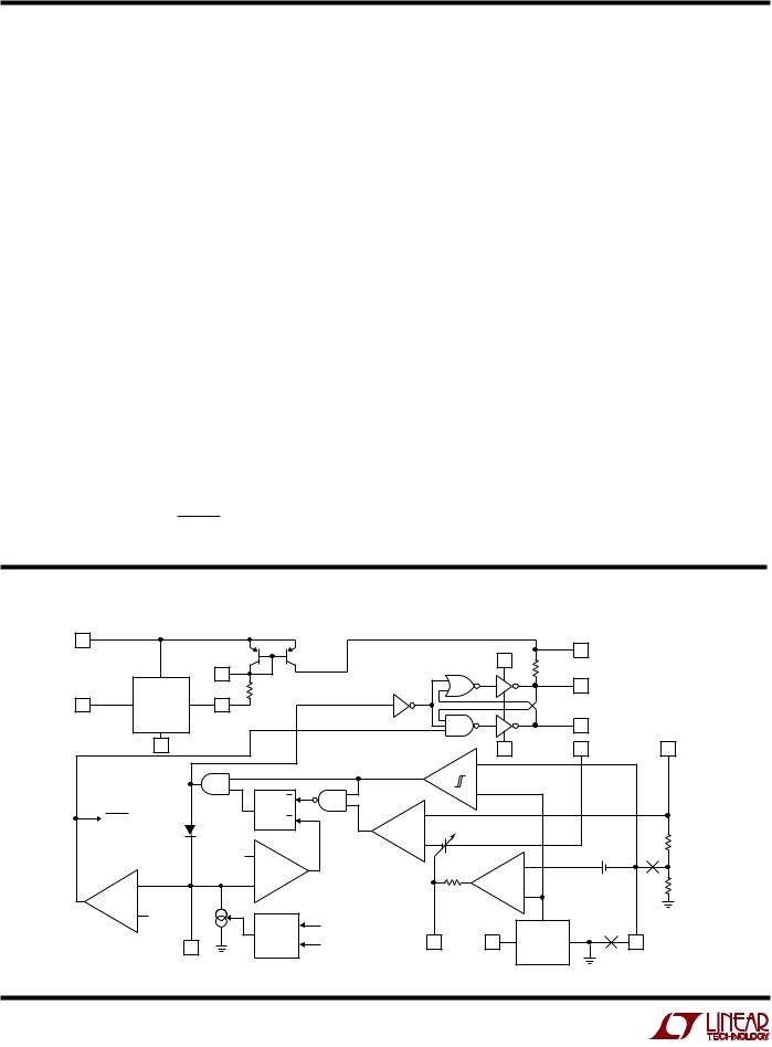
LTC1149 LTC1149-3.3/LTC1149-5
OPERATIOU (Refer to Functional Diagram)
current is made proportional to the output voltage (measured by Pin 8) to model the inductor current, which decays at a rate which is also proportional to the output voltage. While the timing capacitor is discharging, the NGATE output is high, turning on the N-channel MOSFET.
When the voltage on the timing capacitor has discharged past VTH1, comparator T trips, setting the flip-flop. This causes the NGATE output to go low (turning off the N-channel MOSFET) and the PGATE output to also go low (turning the P-channel MOSFET back on). The cycle then repeats.
As the load current increases, the output voltage decreases slightly. This causes the output of the gain stage to increase the current comparator threshold, thus tracking the load current.
The sequence of events for Burst Mode operation is very similar to continuous operation with the cycle interrupted by the voltage comparator. When the output voltage is at orabovethedesiredregulatedvalue,theP-channelMOSFET is held off by comparator V and the timing capacitor continues to discharge below VTH1. When the timing capacitor discharges past VTH2, voltage comparator S
trips, causing the internal SLEEP line to go low and the N-channel MOSFET to turn off.
The circuit now enters sleep mode with both power MOSFETs turned off. In sleep mode, much of the circuitry is turned off, dropping the supply current from several milliamperes (with the MOSFETs switching) to 600μA. When the output capacitor has discharged by the amount of hysteresis in comparator V, the P-channel MOSFET is again turned on and this process repeats. To avoid the operation of the current loop interfering with Burst Mode operation, a built-in offset is incorporated in the gain stage. This prevents the current comparator threshold from increasing until the output voltage has dropped below a minimum threshold.
To prevent both the external MOSFETs from ever being turned on at the same time, feedback is incorporated to sense the state of the driver output pins. Before the N-gate output can go high, the P-drive output must also be high. Likewise, the P-drive output is prevented from going low when the N-gate output is high.
Using constant off-time architecture, the operating frequency is a function of the input voltage. To minimize the frequency variation as dropout is approached, the offtime controller increases the discharge current as VIN drops below VOUT + 1.5V. In dropout the P-channel MOSFET is turned on continuously.
FUUCTIOUAL DIAGRAW Pin 10 connection shown for LTC1149-3.3 and LTC1149-5; changes create LTC1149.
VIN
2 |
|
|
|
|
|
|
|
|
|
1 |
PGATE |
|
|
|
|
|
CAP |
|
|
|
5 |
VCC |
|
|
|
||
|
|
|
|
|
|
500k |
|
|
|
|
|||
|
|
|
16 |
|
|
|
|
|
|
|
|
|
|
|
|
|
|
|
|
|
|
|
4 |
PDRIVE |
|
|
|
SHDN2 |
LOW |
|
VCC |
500k |
|
|
|
|
|
|
|
||
|
|
|
|
|
|
|
|
|
|
||||
15 |
DROPOUT |
3 |
|
|
|
|
|
|
|
|
|
|
|
10V |
|
|
|
|
|
|
|
|
|
|
|
||
|
|
|
|
|
|
|
|
|
|
|
|
|
|
|
REGULATOR |
|
|
|
|
|
|
|
13 |
NGATE |
|
|
|
|
14 |
RGND |
|
|
|
|
12 PGND |
|
9 |
SENSE+ |
8 |
SENSE– |
|
|
|
|
|
|
|
|
– |
|
|
|
|
|
|
|
|
|
|
|
|
|
V |
|
|
|
|
|
|
|
|
|
|
R |
|
|
+ |
|
|
|
|
|
|
|
|
|
|
|
|
|
|
|
|
|
|
|
|
SLEEP |
|
|
|
Q |
|
– |
|
|
|
|
|
|
|
|
|
|
S |
|
|
|
|
|
|
|
|
||
|
|
|
|
C |
|
|
|
|
|
|
|
||
|
|
|
|
|
|
25mV TO 150mV |
|
|
|
|
|
||
|
|
|
|
|
|
+ |
|
|
|
|
|
||
|
|
|
VTH1 |
– |
|
|
|
|
|
VOS |
|
|
|
|
|
|
|
|
|
– |
|
|
|
|
|||
|
|
|
|
T |
|
|
13k |
|
|
|
|
|
|
|
|
|
|
|
|
|
|
|
|
|
|
||
+ |
|
|
|
+ |
|
|
G |
+ |
|
|
|
|
100k |
S |
|
|
|
|
|
|
|
|
|
|
|
|
|
|
|
|
|
|
|
|
|
|
|
|
|
|
|
– |
VTH2 |
|
|
|
VIN |
|
|
|
1.25V |
|
|
|
|
|
|
|
|
OFF-TIME |
|
|
|
|
|
|
|
|
|
|
|
6 |
|
CONTROL |
SENSE– |
7 |
11 |
REFERENCE |
|
10 |
|
|
|
|
|
|
|
|
ITH |
SGND |
|
|
|
SHDN1 |
|
|
|
|
|
CT |
|
|
|
|
|
|
|
|
|||
|
|
|
|
|
|
|
|
|
|
(VFB) |
|
|
|
|
|
|
|
|
|
|
|
|
|
|
|
1149 FD |
|
6
 Loading...