


Linear Technology LTC1199LIS8, LTC1199LCMS8, LTC1199IS8, LTC1199IMS8, LTC1199CS8 Datasheet
...FEATURES
■8-Pin MSOP and SO Packages
■10-Bit Resolution at 500ksps
■Single Supply: 5V or 3V
■Low Power at Full Speed: 25mW Typ at 5V 2.2mW Typ at 2.7V
■Auto Shutdown Reduces Power Linearly at Lower Sample Rates
■10-Bit Upgrade to 8-Bit LTC1196/LTC1198
■SPI and MICROWIRETM Compatible Serial I/O
■Low Cost
APPLICATIOUS
■High Speed Data Acquisition
■Portable or Compact Instrumentation
■Low Power or Battery-Operated Instrumentation
LTC1197/LTC1197L
LTC1199/LTC1199L
10-Bit, 500ksps ADCs in MSOP with Auto Shutdown
DESCRIPTIOU
The LTC®1197/LTC1197L/LTC1199/LTC1199L are 10-bit A/D converters with sampling rates up to 500kHz. They have 2.7V (L) and 5V versions and are offered in 8-pin MSOP and SO packages. Power dissipation is typically only 2.2mW at 2.7V (25mW at 5V) during full speed operation. The automatic power down reduces supply current linearly as sample rate is reduced. These 10-bit, switched-capacitor, successive approximation ADCs include a sample-and-hold. The LTC1197/LTC1197L have a differential analog input with an adjustable reference pin. The LTC1199/LTC1199L offer a software-selectable 2-channel MUX.
The 3-wire serial I/O, MSOP and SO-8 packages, 2.7V operation and extremely high sample rate-to-power ratio make these ADCs ideal choices for compact, low power high speed systems.
These circuits can be used in ratiometric applications or with external references. The high impedance analog inputs and the ability to operate with reduced spans below 1V full scale (LTC1197/LTC1197L) allow direct connection to signal sources in many applications, eliminating the need for gain stages.
 , LTC and LT are registered trademarks of Linear Technology Corporation.
MICROWIRE is a trademark of National Semiconductor Corporation.
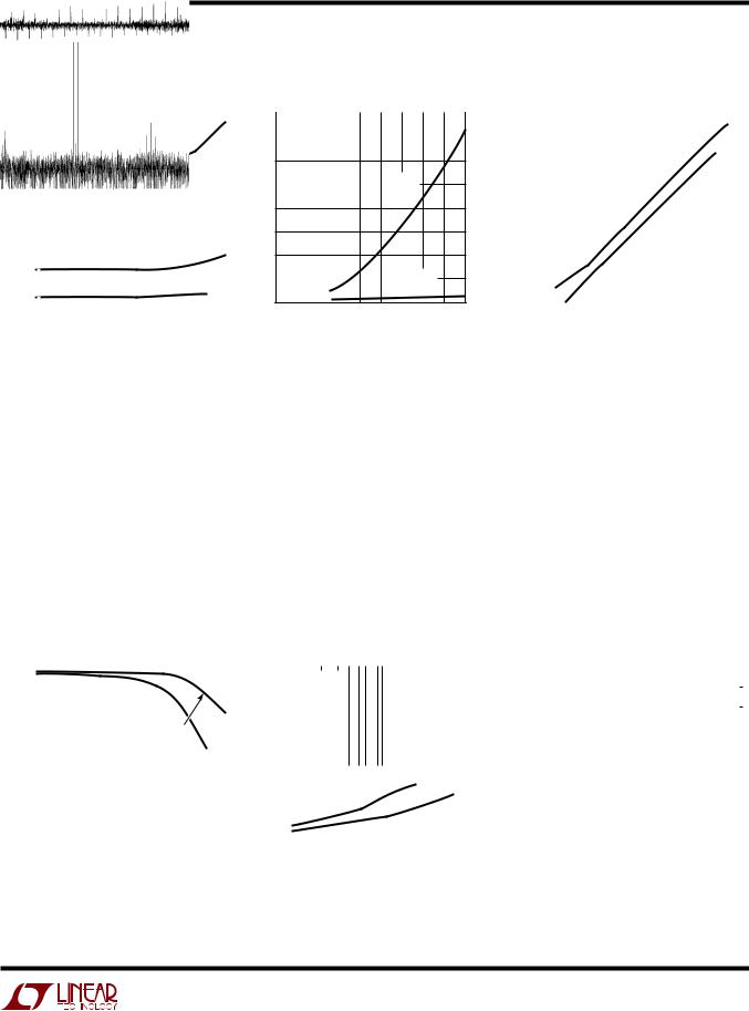
TYPICAL APPLICATIOU
Single 2.7V Supply, 250ksps, 10-Bit Sampling ADC
|
|
|
|
|
|
|
|
|
|
|
|
|
|
|
|
1 F |
|||||
|
|
|
|
|
|
|
|
|
|
|
|
|
|
|
|
|
|
|
|
2.7V |
|
|
|
|
|
|
|
|
|
|
|
|
|
|
|
|
|
|
|
|
|
||
|
|
|
|
|
|
|
|
|
|
|
|
|
|
|
|
|
|
|
|
||
|
|
|
|
|
|
|
|
|
|
|
|
|
|
|
|
|
|
|
|
|
|
|
|
|
|
|
|
|
|
|
|
|
|
|
|
|
|
|
|
|
|
|
|
|
|
|
|
|
|
|
|
|
|
|
|
|
|
|
|
|
|
|
|
|
|
|
|
|
|
|
|
|
|
|
|
|
|
|
|
|
|
|
|
|
|
|
|
|
|
|
|
|
|
|
|
|
LTC1197L |
|
|
|
|||||||||
|
|
|
|
1 |
|
|
|
|
|
|
|
|
|
|
8 |
|
|
|
|||
|
|
|
|
|
|
|
|
|
|
|
|
|
|
|
|
|
|||||
|
|
|
|
CS |
|
|
|
VCC |
|
|
|
||||||||||
|
|
|
|
|
2 |
|
|
|
7 |
|
|
|
|||||||||
ANALOG INPUT |
+IN |
|
|
|
CLK |
|
|
|
|||||||||||||
|
3 |
|
|
|
6 |
|
|
||||||||||||||
|
|
|
|
|
|
|
|
|
|
|
|
|
|||||||||
0V TO 2.7V RANGE |
– IN |
|
|
DOUT |
|
|
|
||||||||||||||
|
|
|
|
4 |
|
|
5 |
|
|
||||||||||||
|
|
|
|
GND |
|
|
|
VREF |
|
|
|
||||||||||
|
|
|
|
|
|
|
|
|
|
|
1197/99 TA01 |
||||||||||
|
|
|
|
|
|
|
|
|
|
|
|
|
|
|
|
|
|
|
|
|
|
|
|
|
|
|
|
|
|
|
|
|
|
|
|
|
|
|
|
|
|
|
|
SERIAL DATA LINK TO ASIC, PLD, MPU, DSP OR SHIFT REGISTERS
Supply Current vs Sampling Frequency
10000
A) |
1000 |
|
|
|
|
|
|
|
|
|
|
|
|
|
|
|
|
|
|
|
|
|
|
||
|
|
|
|
|
VCC = 5V |
|
|
|
|
|||
( |
|
|
|
fCLK = 7.2MHz |
|
|
|
|
||||
CURRENT |
|
|
|
|
|
|
|
|||||
100 |
|
|
|
|
|
|
|
|
|
|
|
|
SUPPLY |
|
|
|
|
|
|
|
|
|
|
|
|
10 |
|
|
|
|
|
fCLK = |
3.5MHz |
|
|
|||
|
|
|
|
|
|
|
|
|
|
|
|
|
|
|
|
|
|
|
|
VCC = 2.7V |
|
|
|
||
|
1 |
|
|
|
|
|
|
|
|
|
|
|
|
|
|
|
|
|
|
|
|
|
|
|
|
|
0.1 |
|
|
|
|
|
|
|
|
|
|
|
|
|
0.1 |
1 |
10 |
100 |
1000 |
||||||
|
0.01 |
|||||||||||
SAMPLING FREQUENCY (kHz)
1197/99 G03
1
LTC1197/LTC1197L
LTC1199/LTC1199L
ABSOLUTE
WAXIWUW
RATIUGS (Notes 1, 2)
Supply Voltage (VCC) ............................................... |
12V |
Operating Temperature Range |
|
Voltage |
|
LTC1197C/LTC1197LC |
0°C to 70°C |
Analog Input ..................... |
GND – 0.3V to VCC + 0.3V |
LTC1199C/LTC1199LC........................... |
|
Digital Input ................................ |
GND – 0.3V to 12V |
LTC1197I/LTC1197LI |
– 45°C to 85°C |
Digital Output .................... |
GND – 0.3V to VCC + 0.3V |
LTC1199I/LTC1199LI ........................ |
|
Power Dissipation .............................................. |
500mW |
Lead Temperature (Soldering, 10 sec)................. |
300°C |
Storage Temperature Range ................. |
– 65°C to 150°C |
|
|
PACKAGE/ORDER IUFORWATIOU
|
|
|
|
ORDER PART |
|
|
|
|
|
|
|
|
ORDER PART |
|||
|
|
|
|
NUMBER |
|
|
|
|
|
TOP VIEW |
|
NUMBER |
||||
|
|
TOP VIEW |
|
|
|
|
|
|
|
|
|
|
|
|
|
|
|
|
|
LTC1197CMS8 |
|
|
|
|
|
|
|
|
LTC1197CS8 |
||||
|
|
|
CS |
1 |
|
|
8 |
VCC |
||||||||
|
|
|
|
|
|
|||||||||||
CS |
1 |
8 VCC |
|
|
|
|
|
|
|
|
||||||
LTC1197IMS8 |
+IN |
2 |
|
|
7 |
CLK |
LTC1197IS8 |
|||||||||
+IN |
2 |
7 CLK |
|
|
||||||||||||
|
|
|
|
|||||||||||||
–IN |
3 |
6 DOUT |
LTC1197LCMS8 |
– IN |
3 |
|
|
6 |
DOUT |
LTC1197LCS8 |
||||||
GND |
4 |
5 VREF |
|
|
|
|
|
|
|
|||||||
LTC1197LIMS8 |
GND |
4 |
|
|
5 |
VREF |
LTC1197LIS8 |
|||||||||
|
|
MS8 PACKAGE |
|
|
|
|
|
|
|
|
||||||
|
|
8-LEAD PLASTIC MSOP |
|
|
|
|
|
|
S8 PACKAGE |
|
|
|
||||
|
|
MS8 PART MARKING |
|
|
|
|
|
S8 PART MARKING |
||||||||
TJMAX = 150°C, θJA = 210°C/W |
|
|
|
8-LEAD PLASTIC SO |
|
|||||||||||
|
|
|
|
LTKV |
LTBL |
|
TJMAX = 150°C, θJA = 175°C/W |
1197 |
1197L |
|||||||
|
|
|
|
LTKW |
LTJA |
|
|
|
|
|
|
|
|
1197I |
1197LI |
|
|
|
|
|
|
|
|
|
|
|
|
|
|
|
|||
|
|
|
|
ORDER PART |
|
|
|
|
|
|
|
|
ORDER PART |
|||
|
|
TOP VIEW |
|
NUMBER |
|
|
|
|
|
TOP VIEW |
|
NUMBER |
||||
|
|
|
LTC1199CMS8 |
|
|
|
|
|
|
|
|
LTC1199CS8 |
||||
|
|
|
8 VCC |
CS |
1 |
|
|
8 |
VCC |
|||||||
CS |
1 |
|||||||||||||||
|
|
|
|
|
|
|
||||||||||
CH0 |
2 |
7 CLK |
LTC1199IMS8 |
CH0 |
2 |
|
|
7 |
CLK |
LTC1199IS8 |
||||||
CH1 |
3 |
6 DOUT |
LTC1199LCMS8 |
|
|
|
|
|
|
|
|
LTC1199LCS8 |
||||
CH1 |
3 |
|
|
6 |
DOUT |
|||||||||||
GND |
4 |
5 DIN |
|
|
||||||||||||
|
|
|
|
LTC1199LIMS8 |
|
|
|
|
|
|
|
|
LTC1199LIS8 |
|||
|
|
MS8 PACKAGE |
|
GND |
4 |
|
|
5 |
DIN |
|||||||
|
|
|
|
|
|
|
|
|
|
|||||||
|
|
8-LEAD PLASTIC MSOP |
|
|
|
|
|
|
S8 PACKAGE |
|
|
|
||||
|
|
MS8 PART MARKING |
|
|
|
|
|
S8 PART MARKING |
||||||||
TJMAX = 150°C, θJA = 210°C/W |
|
|
|
|
|
|||||||||||
|
|
|
8-LEAD PLASTIC SO |
|
||||||||||||
|
|
|
|
LTFL |
LTCM |
|
TJMAX = 150°C, θJA = 175°C/W |
1199 |
1199L |
|||||||
|
|
|
|
LTWB |
LTWC |
|
|
|
|
|
|
|
|
1199I |
1199LI |
|
|
|
|
|
|
|
|
|
|
|
|
|
|
|
|
|
|
Consult factory for parts specified with wider operating temperature ranges.
RECOWWEUDED OPERATIUG COUDITIOUS The ● denotes the specifications which apply over the full operating temperature range, otherwise specifications are at TA = 25°C.
|
|
|
|
|
|
|
|
|
LTC1197 |
|
|
LTC1199 |
|
|
|
SYMBOL |
PARAMETER |
CONDITIONS |
MIN |
TYP |
MAX |
MIN |
TYP |
MAX |
|
UNITS |
|||||
|
|
|
|
|
|
|
|
|
|
|
|
|
|
|
|
VCC |
Supply Voltage |
|
|
4 |
|
9 |
4 |
|
6 |
|
V |
||||
VCC = 5V |
Operation |
|
|
|
|
|
|
|
|
|
|
||||
fCLK |
Clock Frequency |
|
● |
0.05 |
|
7.2 |
0.05 |
|
7.2 |
|
MHz |
||||
tCYC |
Total Cycle Time |
|
|
14 |
|
|
16 |
|
|
|
CLK |
||||
tSMPL |
Analog Input Sampling Time |
|
|
1.5 |
|
|
1.5 |
|
|
|
CLK |
||||
thCS |
|
|
Hold Time |
|
Low After Last CLK↑ |
|
|
13 |
|
|
13 |
|
|
|
ns |
|
CS |
|
|
|
|
|
|
|
|||||||
2

LTC1197/LTC1197L
LTC1199/LTC1199L
RECOWWEUDED OPERATIUG COUDITIOUS The ● denotes the specifications which apply over the full operating temperature range, otherwise specifications are at TA = 25°C.
|
|
|
|
|
|
|
|
|
|
|
|
LTC1197 |
|
|
LTC1199 |
|
|
|
SYMBOL |
|
PARAMETER |
CONDITIONS |
|
MIN |
TYP |
MAX |
MIN |
TYP |
MAX |
|
UNITS |
||||||
VCC = 5V |
Operation |
|
|
|
|
|
|
|
|
|
|
|||||||
tsuCS |
|
|
|
Setup Time |
CS |
↓ Before First CLK↑ |
|
|
26 |
|
|
26 |
|
|
|
ns |
||
|
|
|
|
|
(See Figures 1, 2) |
|
|
|
|
|
|
|
|
|
|
|||
thDI |
|
Hold Time DIN After CLK↑ |
LTC1199 |
|
|
|
|
26 |
|
|
|
ns |
||||||
tsuDI |
|
Setup Time DIN Stable Before CLK↑ |
LTC1199 |
|
|
|
|
26 |
|
|
|
ns |
||||||
tWHCLK |
|
CLK High Time |
fCLK = fCLK(MAX) |
|
40% |
|
|
40% |
|
|
|
1/fCLK |
||||||
tWLCLK |
|
CLK Low Time |
fCLK = fCLK(MAX) |
|
40% |
|
|
40% |
|
|
|
1/fCLK |
||||||
|
|
|
|
|
|
|
|
|
|
|
|
|
|
|
|
|
|
|
tWHCS |
|
|
|
CS |
High Time Between Data Transfer Cycles |
|
|
32 |
|
|
32 |
|
|
|
ns |
|||
|
|
|
|
|
|
Low Time During Data Transfer |
|
|
13 |
|
|
15 |
|
|
|
CLK |
||
tWLCS |
|
|
|
CS |
|
|
|
|
|
|
|
|||||||
|
|
|
|
|
|
|
|
|
|
|
|
|
|
LTC1197L |
|
|
LTC1199L |
|
|
|
SYMBOL |
|
PARAMETER |
CONDITIONS |
MIN |
TYP |
MAX |
MIN |
TYP |
MAX |
|
UNITS |
|||||||||
|
|
|
|
|
|
|
|
|
|
|
|
|
|
|
|
|
|
|
|
|
VCC |
|
Supply Voltage |
|
|
2.7 |
|
4 |
2.7 |
|
4 |
|
V |
||||||||
VCC = 2.7V Operation |
|
|
|
|
|
|
|
|
|
|
||||||||||
fCLK |
|
Clock Frequency |
|
● |
0.01 |
|
3.5 |
0.01 |
|
3.5 |
|
MHz |
||||||||
tCYC |
|
Total Cycle Time |
|
|
14 |
|
|
16 |
|
|
|
CLK |
||||||||
tSMPL |
|
Analog Input Sampling Time |
|
|
1.5 |
|
|
1.5 |
|
|
|
CLK |
||||||||
thCS |
|
|
|
|
Hold Time |
|
|
Low After Last CLK↑ |
|
|
40 |
|
|
40 |
|
|
|
ns |
||
|
|
|
CS |
|
|
|
|
|
|
|
||||||||||
tsuCS |
|
|
|
Setup Time |
|
|
↓ Before First CLK↑ |
|
|
78 |
|
|
78 |
|
|
|
ns |
|||
|
|
|
CS |
|
|
|
|
|
|
|
||||||||||
|
|
|
|
|
(See Figures 1, 2) |
|
|
|
|
|
|
|
|
|
|
|||||
thDI |
|
Hold Time DIN After CLK↑ |
LTC1199L |
|
|
|
|
78 |
|
|
|
ns |
||||||||
tsuDI |
|
Setup Time DIN Stable Before CLK↑ |
LTC1199L |
|
|
|
|
78 |
|
|
|
ns |
||||||||
tWHCLK |
|
CLK High Time |
fCLK = fCLK(MAX) |
|
40% |
|
|
40% |
|
|
|
1/fCLK |
||||||||
tWLCLK |
|
CLK Low Time |
fCLK = fCLK(MAX) |
|
40% |
|
|
40% |
|
|
|
1/fCLK |
||||||||
|
|
|
|
|
High Time Between Data Transfer Cycles |
|
|
96 |
|
|
96 |
|
|
|
ns |
|||||
tWHCS |
|
CS |
|
|
|
|
|
|
|
|||||||||||
|
|
|
|
|
|
Low Time During Data Transfer |
|
|
13 |
|
|
15 |
|
|
|
CLK |
||||
tWLCS |
|
|
CS |
|
|
|
|
|
|
|
||||||||||
COUVERTER AUD WULTIPLEXER CHARACTERISTICS
The ● denotes the specifications which apply over the full operating temperature range, otherwise specifications are at TA = 25°C.
VCC = 5V, VREF = 5V, fCLK = fCLK(MAX) as defined in Recommended Operating Conditions, unless otherwise noted.
|
|
|
|
LTC1197 |
|
LTC1199 |
|
|
|
PARAMETER |
CONDITIONS |
|
MIN |
TYP |
MAX |
MIN |
TYP |
MAX |
UNITS |
Offset Error |
|
● |
|
|
±2 |
|
|
±2 |
LSB |
Linearity Error |
(Note 3) |
● |
|
|
±1 |
|
|
±1 |
LSB |
Gain Error |
|
● |
|
|
±4 |
|
|
±4 |
LSB |
No Missing Codes Resolution |
|
● |
10 |
|
|
10 |
|
|
Bits |
|
|
|
|
|
|
|
|
|
|
Analog Input Range |
|
|
|
|
– 0.05V to VCC + 0.05V |
|
V |
||
Reference Input Range |
LTC1197, VCC ≤ 6V |
|
0.2 |
|
VCC + 0.05V |
|
|
|
V |
|
LTC1197, VCC > 6V |
|
0.2 |
|
6 |
|
|
|
V |
Analog Input Leakage Current |
(Note 4) |
● |
|
|
±1 |
|
|
±1 |
µA |
|
|
|
|
|
|
|
|
|
|
3

LTC1197/LTC1197L
LTC1199/LTC1199L
COUVERTER AUD WULTIPLEXER CHARACTERISTICS
The ● denotes the specifications which apply over the full operating temperature range, otherwise specifications are at TA = 25°C.
VCC = 2.7V, VREF = 2.5V (LTC1197L), fCLK = fCLK(MAX) as defined in Recommended Operating Conditions, unless otherwise noted.
|
|
|
|
LTC1197L |
|
LTC1199L |
|
|
|
PARAMETER |
CONDITIONS |
|
MIN |
TYP |
MAX |
MIN |
TYP |
MAX |
UNITS |
Offset Error |
|
● |
|
|
±2 |
|
|
±2 |
LSB |
|
|
|
|
|
|
|
|
|
|
Linearity Error |
(Note 3) |
● |
|
|
±1 |
|
|
±1 |
LSB |
|
|
|
|
|
|
|
|
|
|
Gain Error |
|
● |
|
|
±4 |
|
|
±4 |
LSB |
|
|
|
|
|
|
|
|
|
|
No Missing Codes Resolution |
|
● |
10 |
|
|
10 |
|
|
Bits |
|
|
|
|
|
|
|
|
|
|
Analog Input Range |
|
|
|
|
– 0.05V to VCC + 0.05V |
|
V |
||
Reference Input Range |
LTC1197L |
|
0.2 |
|
VCC + 0.05V |
|
|
|
V |
Analog Input Leakage Current |
(Note 4) |
● |
|
|
±1 |
|
|
±1 |
A |
|
|
|
|
|
|
|
|
|
|
DYUAWIC ACCURACY
VCC = 5V, VREF = 5V, fCLK = fCLK(MAX) as defined in Recommended Operating Conditions, unless otherwise noted.
|
|
|
|
LTC1197 |
|
|
LTC1199 |
|
|
SYMBOL |
PARAMETER |
CONDITIONS |
MIN |
TYP |
MAX |
MIN |
TYP |
MAX |
UNITS |
S/(N + D) |
Signal-to-Noise Plus |
100kHz Input Signal |
|
60 |
|
|
60 |
|
dB |
|
Distortion Ratio |
|
|
|
|
|
|
|
|
|
|
|
|
|
|
|
|
|
|
THD |
Total Harmonic Distortion |
100kHz Input Signal |
|
– 64 |
|
|
– 64 |
|
dB |
|
First 5 Harmonics |
|
|
|
|
|
|
|
|
|
|
|
|
|
|
|
|
|
|
|
Peak Harmonic or Spurious Noise |
100kHz Input Signal |
|
– 68 |
|
|
– 68 |
|
dB |
|
|
|
|
|
|
|
|
|
|
IMD |
Intermodulation Distortion |
fIN1 = 97.046kHz, fIN2 = 102.905kHz |
|
|
|
|
|
|
|
|
|
2nd Order Terms |
|
– 65 |
|
|
– 65 |
|
dB |
|
|
3rd Order Terms |
|
– 70 |
|
|
– 70 |
|
dB |
|
|
|
|
|
|
|
|
|
|
VCC = 2.7V, VREF = 2.5V, fCLK = fCLK(MAX) as defined in Recommended Operating Conditions, unless otherwise noted.
|
|
|
|
LTC1197L |
|
|
LTC1199L |
|
|
SYMBOL |
PARAMETER |
CONDITIONS |
MIN |
TYP |
MAX |
MIN |
TYP |
MAX |
UNITS |
|
|
|
|
|
|
|
|
|
|
S/(N + D) |
Signal-to-Noise Plus |
50kHz Input Signal |
|
58 |
|
|
58 |
|
dB |
|
Distortion Ratio |
|
|
|
|
|
|
|
|
|
|
|
|
|
|
|
|
|
|
THD |
Total Harmonic Distortion |
50kHz Input Signal |
|
– 60 |
|
|
– 60 |
|
dB |
|
First 5 Harmonics |
|
|
|
|
|
|
|
|
|
|
|
|
|
|
|
|
|
|
|
Peak Harmonic or Spurious Noise |
50kHz Input Signal |
|
– 63 |
|
|
– 63 |
|
dB |
|
|
|
|
|
|
|
|
|
|
IMD |
Intermodulation Distortion |
fIN1 = 48.5kHz, fIN2 = 51.5kHz |
|
|
|
|
|
|
|
|
|
2nd Order Terms |
|
– 60 |
|
|
– 60 |
|
dB |
|
|
3rd Order Terms |
|
– 65 |
|
|
– 65 |
|
dB |
|
|
|
|
|
|
|
|
|
|
4

LTC1197/LTC1197L
LTC1199/LTC1199L
DIGITAL AND DC ELECTRICAL CHARACTERISTICS |
The ● denotes the specifications which apply |
U |
over the full operating temperature range, otherwise specifications are at TA = 25°C. VCC = 5V, VREF = 5V, unless otherwise noted.
|
|
|
|
|
|
|
|
LTC1197 |
|
|
LTC1199 |
|
|
SYMBOL |
PARAMETER |
|
CONDITIONS |
|
MIN |
TYP |
MAX |
MIN |
TYP |
MAX |
UNITS |
||
|
|
|
|
|
|
|
|
|
|
|
|
|
|
VIH |
High Level Input Voltage |
|
VCC = 5.25V |
● |
2.4 |
|
|
2.4 |
|
|
V |
||
VIL |
Low Level Input Voltage |
|
VCC = 4.75V |
● |
|
|
0.8 |
|
|
0.8 |
V |
||
IIH |
High Level Input Current |
|
VIN = VCC |
● |
|
|
2.5 |
|
|
2.5 |
A |
||
IIL |
Low Level Input Current |
|
VIN = 0V |
● |
|
|
– 2.5 |
|
|
– 2.5 |
A |
||
VOH |
High Level Output Voltage |
|
VCC = 4.75V, IO = 10 A |
● |
4.5 |
4.74 |
|
4.5 |
4.74 |
|
V |
||
|
|
|
VCC = 4.75V, IO = 360 A |
● |
2.4 |
4.72 |
|
2.4 |
4.72 |
|
V |
||
VOL |
Low Level Output Voltage |
|
VCC = 4.75V, IO = 1.6mA |
● |
|
|
0.4 |
|
|
0.4 |
V |
||
IOZ |
Hi-Z Output Leakage |
|
|
= High |
|
|
|
±3 |
|
|
±3 |
A |
|
|
CS |
|
● |
|
|
|
|
||||||
ISOURCE |
Output Source Current |
|
VOUT = 0V |
|
|
– 25 |
|
|
– 25 |
|
mA |
||
ISINK |
Output Sink Current |
|
VOUT = VCC |
|
|
45 |
|
|
45 |
|
mA |
||
IREF |
Reference Current (LTC1197) |
|
|
= VCC |
|
|
0.001 |
3 |
|
|
|
A |
|
|
CS |
|
● |
|
|
|
|
||||||
|
|
|
fSMPL = fSMPL(MAX) |
● |
|
0.5 |
1 |
|
|
|
mA |
||
ICC |
Supply Current |
|
|
|
|
0.001 |
3 |
|
0.001 |
3 |
A |
||
|
CS |
= VCC |
● |
|
|
||||||||
|
|
|
fSMPL = fSMPL(MAX) |
● |
|
4.5 |
8 |
|
5 |
8.5 |
mA |
||
PD |
Power Dissipation |
|
fSMPL = fSMPL(MAX) |
|
|
22.5 |
|
|
25 |
|
mW |
||
The ● denotes the specifications which apply over the full operating temperature range, otherwise specifications are at TA = 25°C.
VCC = 2.7V, VREF = 2.5V, unless otherwise noted.
|
|
|
|
|
|
|
|
LTC1197L |
|
|
LTC1199L |
|
|
SYMBOL |
PARAMETER |
|
CONDITIONS |
|
MIN |
TYP |
MAX |
MIN |
TYP |
MAX |
UNITS |
||
VIH |
High Level Input Voltage |
|
VCC = 3.6V |
● |
1.9 |
|
|
1.9 |
|
|
V |
||
VIL |
Low Level Input Voltage |
|
VCC = 2.7V |
● |
|
|
0.45 |
|
|
0.45 |
V |
||
IIH |
High Level Input Current |
|
VIN = VCC |
● |
|
|
2.5 |
|
|
2.5 |
A |
||
IIL |
Low Level Input Current |
|
VIN = 0V |
● |
|
|
– 2.5 |
|
|
– 2.5 |
A |
||
VOH |
High Level Output Voltage |
|
VCC = 2.7V, IO = 10 A |
● |
2.3 |
2.60 |
|
2.3 |
2.60 |
|
V |
||
|
|
|
VCC = 2.7V, IO = 360 A |
● |
2.1 |
2.45 |
|
2.1 |
2.45 |
|
V |
||
VOL |
Low Level Output Voltage |
|
VCC = 2.7V, IO = 400 A |
● |
|
|
0.3 |
|
|
0.3 |
V |
||
IOZ |
Hi-Z Output Leakage |
|
|
= High |
|
|
|
±3 |
|
|
±3 |
A |
|
|
CS |
|
● |
|
|
|
|
||||||
ISOURCE |
Output Source Current |
|
VOUT = 0V |
|
|
– 6.5 |
|
|
– 6.5 |
|
mA |
||
ISINK |
Output Sink Current |
|
VOUT = VCC |
|
|
11 |
|
|
11 |
|
mA |
||
IREF |
Reference Current (LTC1197L) |
|
|
|
= VCC |
|
|
0.001 |
3.0 |
|
|
|
A |
|
CS |
● |
|
|
|
|
|||||||
|
|
|
fSMPL = fSMPL(MAX) |
● |
|
0.250 |
0.5 |
|
|
|
mA |
||
ICC |
Supply Current |
|
|
= VCC |
|
|
0.001 |
3 |
|
0.001 |
3 |
A |
|
|
CS |
● |
|
|
|||||||||
|
|
|
fSMPL = fSMPL(MAX) |
● |
|
0.8 |
2 |
|
0.8 |
2 |
mA |
||
PD |
Power Dissipation |
|
fSMPL = fSMPL(MAX) |
|
|
2.2 |
|
|
2.2 |
|
mW |
||
5

LTC1197/LTC1197L
LTC1199/LTC1199L
AC CHARACTERISTICS
The ● denotes the specifications which apply over the full operating temperature range, otherwise specifications are at TA = 25°C.
VCC = 5V, VREF = 5V, fCLK = fCLK(MAX) as defined in Recommended Operating Conditions, unless otherwise noted.
|
|
|
|
|
|
|
LTC1197 |
|
|
LTC1199 |
|
|
SYMBOL |
PARAMETER |
CONDITIONS |
|
MIN |
TYP |
MAX |
MIN |
TYP |
MAX |
UNITS |
||
|
|
|
|
|
|
|
|
|
|
|
|
|
tCONV |
Conversion Time (See Figures 1, 2) |
|
● |
|
|
1.4 |
|
|
1.4 |
µs |
||
fSMPL(MAX) |
Maximum Sampling Frequency |
|
● |
500 |
|
|
450 |
|
|
kHz |
||
tdDO |
Delay Time, CLK↑ to DOUT Data Valid |
CLOAD = 20pF |
|
|
68 |
78 |
|
68 |
78 |
ns |
||
|
|
|
|
|
● |
|
|
100 |
|
|
100 |
ns |
tdis |
Delay Time, |
|
↑ to DOUT Hi-Z |
|
|
|
75 |
150 |
|
75 |
150 |
ns |
CS |
|
● |
|
|
||||||||
ten |
Delay Time, CLK↓ to DOUT Enabled |
CLOAD = 20pF |
● |
|
40 |
68 |
|
40 |
68 |
ns |
||
thDO |
Time Output Data Remains |
CLOAD = 20pF |
● |
15 |
55 |
|
15 |
55 |
|
ns |
||
|
Valid After CLK↑ |
|
|
|
|
|
|
|
|
|
||
tr |
DOUT Rise Time |
CLOAD = 20pF |
● |
|
10 |
20 |
|
10 |
20 |
ns |
||
tf |
DOUT Fall Time |
CLOAD = 20pF |
● |
|
10 |
20 |
|
10 |
20 |
ns |
||
CIN |
Input Capacitance |
Analog Input On Channel |
|
|
20 |
|
|
20 |
|
pF |
||
|
|
|
|
Analog Input Off Channel |
|
|
5 |
|
|
5 |
|
pF |
|
|
|
|
Digital Input |
|
|
5 |
|
|
5 |
|
pF |
The ● denotes the specifications which apply over the full operating temperature range, otherwise specifications are at TA = 25°C.
VCC = 2.7V, VREF = 2.5V, fCLK = fCLK(MAX) as defined in Recommended Operating Conditions, unless otherwise noted.
|
|
|
|
|
|
|
LTC1197L |
|
|
LTC1199L |
|
|
SYMBOL |
PARAMETER |
CONDITIONS |
|
MIN |
TYP |
MAX |
MIN |
TYP |
MAX |
UNITS |
||
|
|
|
|
|
|
|
|
|
|
|
|
|
tCONV |
Conversion Time (See Figures 1, 2) |
|
● |
|
|
2.9 |
|
|
2.9 |
µs |
||
fSMPL(MAX) |
Maximum Sampling Frequency |
|
● |
250 |
|
|
210 |
|
|
kHz |
||
tdDO |
Delay Time, CLK↑ to DOUT Data Valid |
CLOAD = 20pF |
|
|
130 |
180 |
|
130 |
180 |
ns |
||
|
|
|
|
|
● |
|
|
250 |
|
|
250 |
ns |
tdis |
Delay Time, |
|
↑ to DOUT Hi-Z |
|
|
|
120 |
250 |
|
120 |
250 |
ns |
CS |
|
● |
|
|
||||||||
ten |
Delay Time, CLK↓ to DOUT Enabled |
CLOAD = 20pF |
● |
|
100 |
200 |
|
100 |
200 |
ns |
||
thDO |
Time Output Data Remains |
CLOAD = 20pF |
● |
30 |
120 |
|
30 |
120 |
|
ns |
||
|
Valid After CLK↑ |
|
|
|
|
|
|
|
|
|
||
tr |
DOUT Rise Time |
CLOAD = 20pF |
● |
|
15 |
40 |
|
15 |
40 |
ns |
||
tf |
DOUT Fall Time |
CLOAD = 20pF |
● |
|
15 |
40 |
|
15 |
40 |
ns |
||
CIN |
Input Capacitance |
Analog Input On Channel |
|
|
20 |
|
|
20 |
|
pF |
||
|
|
|
|
Analog Input Off Channel |
|
|
5 |
|
|
5 |
|
pF |
|
|
|
|
Digital Input |
|
|
5 |
|
|
5 |
|
pF |
Note 1: Absolute Maximum Ratings are those values beyond which the life of a device may be impaired.
Note 2: All voltage values are with respect to GND.
Note 3: Integral nonlinearity is defined as deviation of a code from a straight line passing through the actual endpoints of the transfer curve. The deviation is measured from the center of the quantization band.
Note 4: Channel leakage current is measured after the channel selection.
6
LTC1197/LTC1197L
LTC1199/LTC1199L
TYPICAL PERFORWAUCE CHARACTERISTICS
SUPPLY CURRENT (mA)
|
Supply Current vs Clock Rate* |
|
|
|
|
|||||||||||||||||||||
20 |
|
|
|
|
|
|
|
|
|
|
|
|
|
|
|
|
|
|
|
|
|
|
|
|
|
|
|
|
|
|
|
|
|
|
|
|
|
|
|
|
|
|
|
|
|
|
|
|
|
|
|
|
|
18 |
|
|
|
|
|
|
|
|
|
|
|
|
|
|
|
|
|
|
|
|
|
|
|
|
|
|
|
|
|
|
|
|
|
|
|
|
|
|
|
|
|
|
|
|
|
|
|
|
|
|
|
|
|
16 |
|
|
|
|
|
|
|
|
|
|
|
VCC = 9V |
|
|
|
|
|
|
|
|
|
(mA) |
||||
|
|
|
|
|
|
|
|
|
|
|
|
|
|
|
|
|
|
|
|
|||||||
14 |
|
|
|
|
|
|
|
|
|
|
|
|
|
|
|
|
|
|
|
|
|
|
|
|
|
|
|
|
|
|
|
|
|
|
|
|
|
|
|
|
|
|
|
|
|
|
|
|
|
|
|
||
12 |
|
|
|
|
|
|
|
|
|
|
|
|
|
|
|
|
|
|
|
|
|
|
|
|
|
CURRENT |
|
|
|
|
|
|
|
|
|
|
|
|
|
|
|
|
|
|
|
|
|
|
|
|
|
|
|
10 |
|
|
|
|
|
|
|
|
|
|
|
|
|
|
|
|
|
|
|
|
|
|
|
|
|
SUPPLY |
|
|
|
|
|
|
|
|
|
|
|
|
|
|
|
|
|
|
|
|
|
|
|
|
|
||
8 |
|
|
|
|
|
|
|
|
|
|
|
|
|
|
|
|
|
|
|
|
|
|
|
|
|
|
|
|
|
|
|
|
|
|
|
|
|
|
|
|
|
|
|
|
|
|
|
|
|
|
|
|
|
6 |
|
|
|
|
|
|
|
|
|
|
|
|
|
|
|
|
|
|
|
|
|
|
|
|
|
|
|
|
|
|
|
|
|
|
|
|
|
|
|
|
|
|
|
|
|
|
|
|
|
|
|
|
|
4 |
|
|
|
|
|
|
|
|
|
|
|
VCC = 5V |
|
|
|
|
|
|
|
|
|
|
||||
|
|
|
|
|
|
|
|
|
|
|
|
|
|
|
|
|
|
|
|
|
||||||
2 |
|
|
|
|
|
|
|
|
|
|
|
|
|
|
|
|
|
|
|
|
|
|
|
|
|
|
|
|
|
|
|
|
|
|
VCC = 2.7V |
|
|
|
|
|
|
|
|
|
|||||||||
|
|
|
|
|
|
|
|
|
|
|
|
|
|
|
|
|
|
|||||||||
|
|
|
|
|
|
|
|
|
|
|
|
|
|
|
|
|
|
|
||||||||
0 |
|
|
|
|
|
|
|
|
|
|
|
|
|
|
|
|
|
|
|
|
|
|
|
|
|
|
|
|
|
|
|
|
100 |
1000 |
|
|
|
|
10000 |
||||||||||||||
10 |
|
|
|
|
|
|
|
|
|
|||||||||||||||||
FREQUENCY (kHz)
1197/99 G01
Supply Current vs Supply Voltage
16 |
|
|
|
|
|
|
|
|
|
80 |
|
fCLK = 3.5MHz |
|
||||||||
|
|
|
|
|||||||
14 |
|
TA = 25°C |
|
70 |
||||||
|
|
|||||||||
12 |
|
|
|
|
|
|
|
|
|
|
|
|
|
|
|
|
|
|
|
|
|||
10 |
|
|
|
|
|
|
|
ACTIVE |
|
||
|
|
|
|
|
|
|
MODE |
|
|
||
|
|
|
|
|
|
|
|
|
|||
8 |
|
|
|
|
|
|
|
|
|
|
|
6 |
|
|
|
|
|
|
|
|
|
|
|
4 |
|
|
|
|
|
|
|
|
|
|
|
|
|
|
|
|
|
|
|
|
|
|
|
2 |
|
|
|
|
|
|
|
SHUTDOWN |
|||
|
|
|
|
|
|
|
|||||
|
|
|
|
|
|
|
MODE |
||||
|
|
|
|
|
|
|
|
||||
0 |
|
|
|
|
|
|
|
|
|
|
|
|
|
|
|
|
|
|
|
||||
0 |
1 |
2 |
3 |
4 |
5 |
6 |
7 |
|
|
|
SUPPLY VOLTAGE (V) |
|
|||
60 |
SHUTDOWN |
|
|
||
50 |
CURRENT |
|
40 |
||
|
||
30 |
(nA) |
|
20 |
||
|
10
0
8 9
1197/99 G02
|
|
Supply Current |
|
|
|
|
||||||||
|
|
vs Sampling Frequency |
|
|
|
|
||||||||
10000 |
|
|
|
|
|
|
|
|
|
|
|
|
|
|
|
|
|
|
|
|
|
|
|
|
|
|
|
||
A) |
1000 |
|
|
|
|
|
|
|
|
|
|
|
|
|
|
|
|
|
|
|
VCC = 5V |
|
|
|
|
|
|||
( |
|
|
|
|
fCLK = 7.2MHz |
|
|
|
|
|
||||
CURRENT |
|
|
|
|
|
|
|
|
|
|||||
100 |
|
|
|
|
|
|
|
|
|
|
|
|
|
|
SUPPLY |
|
|
|
|
|
|
|
|
|
|
|
|
|
|
10 |
|
|
|
|
|
|
fCLK = |
3.5MHz |
|
|
|
|||
|
|
|
|
|
|
|
|
|
|
|
|
|
|
|
|
|
|
|
|
|
|
|
VCC = 2.7V |
|
|
|
|
||
|
1 |
|
|
|
|
|
|
|
|
|
|
|
|
|
|
|
|
|
|
|
|
|
|
|
|
|
|
|
|
|
0.1 |
|
|
|
|
|
|
|
|
|
|
|
|
|
|
|
0.1 |
1 |
10 |
100 |
1000 |
||||||||
|
0.01 |
|||||||||||||
SAMPLING FREQUENCY (kHz)
1197/99 G03
|
INL Plot |
|
|
|
|
|
|
|
|
DNL Plot |
|
|
|
|
|
|
|
||||||
|
1.0 |
|
|
|
|
|
|
|
|
|
|
|
1.0 |
|
|
|
|
|
|
|
|
|
|
|
|
|
VCC = VREF = 5V |
|
|
|
|
|
|
|
|
|
VCC = VREF = 5V |
|
|
|
|
|
|
||||
|
|
|
fCLK = 7.2MHz |
|
|
|
|
|
|
|
|
|
fCLK = 7.2MHz |
|
|
|
|
|
|
||||
|
0.5 |
|
TA = 25°C |
|
|
|
|
|
|
|
|
0.5 |
|
TA = 25°C |
|
|
|
|
|
|
|
||
(LSBs) |
|
|
|
|
|
|
|
|
|
|
(LSBs) |
|
|
|
|
|
|
|
|
|
|
||
0 |
|
|
|
|
|
|
|
|
|
|
0 |
|
|
|
|
|
|
|
|
|
|
||
|
|
|
|
|
|
|
|
|
|
|
|
|
|
|
|
|
|
|
|
||||
INL |
|
|
|
|
|
|
|
|
|
|
|
DNL |
|
|
|
|
|
|
|
|
|
|
|
|
– 0.5 |
|
|
|
|
|
|
|
|
|
|
|
– 0.5 |
|
|
|
|
|
|
|
|
|
|
|
|
|
|
|
|
|
|
|
|
|
|
|
|
|
|
|
|
|
|
|
|
||
|
–1.0 |
|
|
|
|
|
|
|
|
|
|
|
–1.0 |
|
|
|
|
|
|
|
|
|
|
|
0 |
128 |
256 |
384 |
512 |
640 |
768 |
896 |
1024 |
|
0 |
128 |
256 |
384 |
512 |
640 |
768 |
896 |
1024 |
||||
|
|
|
|
|
|
CODE |
|
|
|
|
|
|
|
|
|
|
|
CODE |
|
|
|
|
|
|
|
|
|
|
|
|
|
|
1197/99 G04 |
|
|
|
|
|
|
|
|
|
1197/99 G26 |
||||
|
LTC1197 4096 Point FFT |
|
|
|
|
||||
|
0 |
|
|
|
|
|
|
|
|
|
–10 |
|
|
|
fSMPL = 500kHz |
|
|
|
|
|
|
|
|
fIN = 97.045898kHz |
|
|
|
||
|
|
|
|
|
|
|
|||
|
– 20 |
|
|
|
|
|
|
|
|
|
|
|
|
|
|
|
|
|
|
(dB) |
– 30 |
|
|
|
|
|
|
|
|
|
|
|
|
|
|
|
|
||
– 40 |
|
|
|
|
|
|
|
|
|
AMPLITUDE |
|
|
|
|
|
|
|
|
|
– 50 |
|
|
|
|
|
|
|
|
|
|
|
|
|
|
|
|
|
|
|
|
– 60 |
|
|
|
|
|
|
|
|
|
|
|
|
|
|
|
|
|
|
|
– 70 |
|
|
|
|
|
|
|
|
|
|
|
|
|
|
|
|
|
|
|
– 80 |
|
|
|
|
|
|
|
|
|
|
|
|
|
|
|
|
|
|
|
– 90 |
|
|
|
|
|
|
|
|
|
|
|
|
|
|
|
|
|
|
|
–100 |
|
|
|
|
|
|
|
|
|
|
50 |
100 |
150 |
200 |
250 |
|||
|
0 |
||||||||
FREQUENCY (kHz)
1197/99 G06
|
|
ENOBs vs Frequency |
|
|
THD vs Frequency |
||||||||||||||||||||||||||||||||||||||||||||||||
|
10 |
|
|
|
|
|
|
|
|
|
|
|
|
|
|
|
|
|
|
|
|
|
|
|
|
|
|
|
0 |
|
|
|
|
|
|
|
|
|
|
|
|
|
|
|
|
|
|
|
|
|
|
|
|
|
9 |
|
|
|
|
|
|
|
|
|
|
|
|
|
|
|
|
|
|
|
|
|
|
|
|
|
|
|
– 10 |
TA = |
25°C |
|
|
|
|
|
|
|
|
|
|
|
|
|
|
|
|
|
|
|
|||
|
|
|
|
|
|
|
|
|
|
|
|
|
|
|
|
|
|
|
|
|
|
|
|
|
|
|
|
|
|
|
|
|
|
|
|
|
|
|
|
|
|
|
|
|
|
|
|
|
|
|
|
||
|
|
|
|
|
|
|
|
|
|
|
|
|
|
|
|
|
|
|
|
|
|
|
|
|
|
|
|
|
|
|
|
|
|
|
|
|
|
|
|
|
|
|
|
|
|
|
|
|
|
|
|
||
|
8 |
|
|
|
|
|
|
|
|
|
|
VCC = 2.7V |
|
|
|
|
|
|
|
|
|
|
|
|
|
|
|
|
|
|
|
|
|
|
|
|
|
|
|
|
|
|
|
|
|
||||||||
|
|
|
|
|
|
|
|
|
|
|
|
|
|
|
|
|
|
|
|
|
|
|
|
|
|
|
|
|
|
|
|
|
|
|
|
|
|
|
|
|
|
|
|
|
|||||||||
|
|
|
|
|
|
|
|
|
fSMPL = 250kHz |
|
|
|
|
|
|
|
|
|
– 20 |
|
|
|
|
|
|
|
|
|
|
|
|
|
|
|
|
|
|
|
|
|
|
|
|
||||||||||
|
7 |
|
|
|
|
|
|
|
|
|
|
|
|
|
|
|
|
|
|
|
|
|
|
|
|
|
|
|
|
|
|
|
|
|
|
|
|
|
|
|
|
|
|||||||||||
|
|
|
|
|
|
|
|
|
|
|
|
|
|
VCC = 5V |
|
|
|
|
|
|
|
|
|
|
|
|
|
|
|
|
|
|
|
|
|
|
|
|
|
|
|
|
|
|
|
|
|
||||||
|
|
|
|
|
|
|
|
|
|
|
|
|
|
|
|
|
|
|
|
|
|
|
|
|
|
|
|
|
|
|
|
|
|
|
|
|
|
|
|
|
|
|
|
|
|
|
|||||||
ENOBs |
6 |
|
|
|
|
|
|
|
|
|
|
fSMPL = 500kHz |
|
|
|
|
|
|
|
THD(dB) |
– 30 |
|
|
|
|
|
|
|
|
|
|
|
|
|
|
|
|
|
|
|
|
|
|
|
|
||||||||
|
|
|
|
|
|
|
|
|
|
|
|
|
|
|
|
|
|
|
|
|
|
|
|
|
|
|
|
|
|
|
|
|
|
|
|
|
|
|
|
|
|||||||||||||
|
|
|
|
|
|
|
|
|
|
|
|
|
|
|
|
|
|
|
|
|
|
|
|
|
|
– 40 |
|
|
|
|
|
VCC = |
2.7V |
|
|
|
|
|
|
|
|
|
|
|
|
||||||||
5 |
|
|
|
|
|
|
|
|
|
|
|
|
|
|
|
|
|
|
|
|
|
|
|
|
|
|
|
|
|
|
|
|
|
|
|
|
|
|
|
|
|
|
|
||||||||||
|
|
|
|
|
|
|
|
|
|
|
|
|
|
|
|
|
|
|
|
|
|
|
|
|
|
|
|
|
|
|
|
|
|
|
|
|
|
|
|
|
|
|
|
|
|
|
|
|
|
|
|
||
|
4 |
|
|
|
|
|
|
|
|
|
|
|
|
|
|
|
|
|
|
|
|
|
|
|
|
|
|
|
– 50 |
|
|
|
fSMPL = 250kHz |
|
|
|
|
|
|
|
|
|
|
|
|||||||||
|
|
|
|
|
|
|
|
|
|
|
|
|
|
|
|
|
|
|
|
|
|
|
|
|
|
|
|
||||||||||||||||||||||||||
|
|
|
|
|
|
|
|
|
|
|
|
|
|
|
|
|
|
|
|
|
|
|
|
|
|
|
|
|
|
|
|
|
|
|
|
|
|
|
|
|
|
||||||||||||
|
3 |
|
|
|
|
|
|
|
|
|
|
|
|
|
|
|
|
|
|
|
|
|
|
|
|
|
|
|
– 60 |
|
|
|
|
|
|
|
|
|
|
|
|
|
|
|
|
|
|
|
|
|
|
|
|
|
|
|
|
|
|
|
|
|
|
|
|
|
|
|
|
|
|
|
|
|
|
|
|
|
|
|
|
|
|
|
|
|
|
|
|
|
|
|
|
|
|
|
|
|
|
|
|
|
|
|
|
||
|
2 |
|
|
|
|
|
|
|
|
|
|
|
|
|
|
|
|
|
|
|
|
|
|
|
|
|
|
|
|
|
|
|
|
|
|
|
|
|
|
|
|
|
|
|
|
|
|
|
|
|
|
|
|
|
|
|
|
|
|
|
|
|
|
|
|
|
|
|
|
|
|
|
|
|
|
|
|
|
|
|
|
|
|
|
|
|
|
|
|
|
|
|
|
|
|
|
|
|
|
|
|
|
|
|
|
||
|
|
|
|
|
|
|
|
|
|
|
|
|
|
|
|
|
|
|
|
|
|
|
|
|
|
|
|
– 70 |
|
|
|
|
|
|
|
|
|
|
|
|
|
|
VCC = 5V |
|
|
|
|
||||||
|
|
|
|
|
|
|
|
|
|
|
|
|
|
|
|
|
|
|
|
|
|
|
|
|
|
|
|
|
|
|
|
|
|
|
|
|
|
|
|
|
|
|
|
|
|
||||||||
|
|
|
|
|
|
|
|
|
|
|
|
|
|
|
|
|
|
|
|
|
|
|
|
|
|
|
|
|
|
|
|
|
|
|
|
|
|
|
|
|
|
|
|
|
|
|
|||||||
|
1 |
|
|
|
|
|
|
|
|
|
|
|
|
|
|
|
|
|
|
|
|
|
|
|
|
|
|
|
|
|
|
|
|
|
|
|
|
|
|
|
|
|
fSMPL = 500kHz |
|
|
|
|
|
|||||
|
|
|
|
|
|
|
|
|
|
|
|
|
|
|
|
|
|
|
|
|
|
|
|
|
|
|
|
|
|
|
|
|
|
|
|
|
|
|
|
|
|
|
|
|
|
|
|||||||
|
|
|
|
|
|
|
|
|
|
|
|
|
|
|
|
|
|
|
|
|
|
|
|
|
|
|
|
– 80 |
|
|
|
|
|
|
|
|
|
|
|
|
|
|
|
|
|
|
|
||||||
|
0 |
|
|
|
|
|
|
|
|
|
|
|
|
|
|
|
|
|
|
|
|
|
|
|
|
|
|
|
|
|
|
|
|
|
|
|
|
|
|
|
|
|
|
|
|
|
|
|
|
|
|
|
|
|
|
|
|
|
|
|
|
|
|
|
|
|
|
|
|
|
|
|
|
|
|
|
|
|
|
|
|
|
|
|
|
|
|
|
|
|
|
|
|
|
|
|
|
|
|
|
|
|
|
|
|
||
1 |
10 |
100 |
1000 |
10 |
100 |
1000 |
|
FREQUENCY (kHz) |
|
|
FREQUENCY (kHz) |
|
|
|
|
|
1197/99 G07 |
|
|
1197/99 G08 |
*Part is continuously sampling, spending only a minimum amount of time in shutdown.
|
Intermodulation Distortion Plot |
|
|
|
|||||
|
0 |
|
|
|
|
|
|
|
|
|
–10 |
|
|
|
fSMPL = 500kHz |
|
|
|
|
|
|
|
|
fIN1 = 97.045898kHz |
|
|
|
||
|
|
|
|
|
|
|
|||
|
– 20 |
|
|
|
fIN2 = 102.905273kHz |
|
|
||
|
|
|
|
|
|
|
|
|
|
|
|
|
|
|
|
|
|
|
|
(dB) |
– 30 |
|
|
|
|
|
|
|
|
|
|
|
|
|
|
|
|
||
– 40 |
|
|
|
|
|
|
|
|
|
AMPLITUDE |
|
|
|
|
|
|
|
|
|
– 50 |
|
|
|
|
|
|
|
|
|
|
|
|
|
|
|
|
|
|
|
|
– 60 |
|
|
|
|
|
|
|
|
|
|
|
|
|
|
|
|
|
|
|
– 70 |
|
|
|
|
|
|
|
|
|
|
|
|
|
|
|
|
|
|
|
– 80 |
|
|
|
|
|
|
|
|
|
|
|
|
|
|
|
|
|
|
|
– 90 |
|
|
|
|
|
|
|
|
|
|
|
|
|
|
|
|
|
|
|
–100 |
|
|
|
|
|
|
|
|
|
|
50 |
|
|
|
|
|
|
|
|
0 |
100 |
150 |
200 |
250 |
||||
FREQUENCY (kHz)
1197/99 G09
7
LTC1197/LTC1197L
LTC1199/LTC1199L
TYPICAL PERFORWAUCE CHARACTERISTICS
|
|
LTC1197L Change in Linearity |
|
|
|||||||||||||||||||||
|
|
vs Supply Voltage |
|
|
|
|
|
|
|
|
|
|
|
|
|
||||||||||
|
1.0 |
|
|
|
|
|
|
|
|
|
|
|
|
|
|
|
|
|
|
|
|
|
|
|
|
|
0.8 |
|
VREF = 2.5V |
|
|
|
|
|
|
|
|
|
|
|
|
|
|
|
|
||||||
(LSBs) |
|
fCLK = 3.5MHz |
|
|
|
|
|
|
|
|
|
|
|
|
|
|
|
|
|||||||
|
|
|
|
|
|
|
|
|
|
|
|
|
|
|
|
||||||||||
0.6 |
|
|
|
|
|
|
|
|
|
|
|
|
|
|
|
|
|
|
|
|
|
|
|
|
|
|
|
|
|
|
|
|
|
|
|
|
|
|
|
|
|
|
|
|
|
|
|
|
|
|
|
LINEARITYIN |
0.4 |
|
|
|
|
|
|
|
|
|
|
|
|
|
|
|
|
|
|
|
|
|
|
|
|
|
|
|
|
|
|
|
|
|
|
|
|
|
|
|
|
|
|
|
|
|
|
|
|||
– 0.2 |
|
|
|
|
|
|
|
|
|
|
|
|
|
|
|
|
|
|
|
|
|
|
|
||
|
0.2 |
|
|
|
|
|
|
|
|
|
|
|
|
|
|
|
|
|
|
|
|
|
|
|
|
CHANGE |
0 |
|
|
|
|
|
|
|
|
|
|
|
|
|
|
|
|
|
|
|
|
|
|
|
|
– 0.6 |
|
|
|
|
|
|
|
|
|
|
|
|
|
|
|
|
|
|
|
|
|
|
|
||
|
|
|
|
|
|
|
|
|
|
|
|
|
|
|
|
|
|
|
|
|
|
|
|||
|
– 0.4 |
|
|
|
|
|
|
|
|
|
|
|
|
|
|
|
|
|
|
|
|
|
|
|
|
|
|
|
|
|
|
|
|
|
|
|
|
|
|
|
|
|
|
|
|
|
|
|
|
||
|
– 0.8 |
|
|
|
|
|
|
|
|
|
|
|
|
|
|
|
|
|
|
|
|
|
|
|
|
|
|
|
|
|
|
|
|
|
|
|
|
|
|
|
|
|
|
|
|
|
|
|
|
||
|
|
|
|
|
|
|
|
|
|
|
|
|
|
|
|
|
|
|
|
|
|
|
|
||
|
– 1.0 |
|
|
|
|
|
|
|
|
|
|
|
|
|
|
|
|
|
|
|
|
|
|
|
|
|
|
1 |
|
|
|
|
|
|
3 |
|
|
|
|
4 |
|
|
|
|
|||||||
|
0 |
|
|
|
|
2 |
|
|
|
|
|
|
|
5 |
|||||||||||
|
|
|
|
|
|
|
SUPPLY VOLTAGE (V) |
|
|
|
|
|
|
|
|
||||||||||
|
|
|
|
|
|
|
|
|
|
|
|
|
|
|
|
|
|
|
|
|
1197/99 G10 |
||||
|
LTC1197 Change in Linearity |
|
|
||||||||||||||||||||||
|
vs Supply Voltage |
|
|
|
|
|
|
|
|
|
|
|
|
|
|||||||||||
|
1.0 |
|
|
|
|
|
|
|
|
|
|
|
|
|
|
|
|
|
|
|
|
|
|
|
|
|
0.8 |
|
VREF = 4V |
|
|
|
|
|
|
|
|
|
|
|
|
|
|
|
|
|
|
|
|||
|
|
fCLK = 7MHz |
|
|
|
|
|
|
|
|
|
|
|
|
|
|
|
|
|
|
|||||
|
|
|
|
|
|
|
|
|
|
|
|
|
|
|
|
|
|
|
|
||||||
|
|
|
|
|
|
|
|
|
|
|
|
|
|
|
|
|
|
|
|
|
|||||
(LSBs) |
0.6 |
|
TA = 25°C |
|
|
|
|
|
|
|
|
|
|
|
|
|
|
|
|
|
|
|
|||
|
|
|
|
|
|
|
|
|
|
|
|
|
|
|
|
|
|
|
|
||||||
0.4 |
|
|
|
|
|
|
|
|
|
|
|
|
|
|
|
|
|
|
|
|
|
|
|
|
|
|
|
|
|
|
|
|
|
|
|
|
|
|
|
|
|
|
|
|
|
|
|
|
|
||
LINEARITYIN |
– 0.2 |
|
|
|
|
|
|
|
|
|
|
|
|
|
|
|
|
|
|
|
|
|
|
|
|
|
0.2 |
|
|
|
|
|
|
|
|
|
|
|
|
|
|
|
|
|
|
|
|
|
|
|
|
CHANGE |
0 |
|
|
|
|
|
|
|
|
|
|
|
|
|
|
|
|
|
|
|
|
|
|
|
|
– 0.6 |
|
|
|
|
|
|
|
|
|
|
|
|
|
|
|
|
|
|
|
|
|
|
|
|
|
|
|
|
|
|
|
|
|
|
|
|
|
|
|
|
|
|
|
|
|
|
|
|
|
||
|
– 0.4 |
|
|
|
|
|
|
|
|
|
|
|
|
|
|
|
|
|
|
|
|
|
|
|
|
|
|
|
|
|
|
|
|
|
|
|
|
|
|
|
|
|
|
|
|
|
|
|
|
|
|
|
– 0.8 |
|
|
|
|
|
|
|
|
|
|
|
|
|
|
|
|
|
|
|
|
|
|
|
|
|
|
|
|
|
|
|
|
|
|
|
|
|
|
|
|
|
|
|
|
|
|
|
|
|
|
|
|
|
|
|
|
|
|
|
|
|
|
|
|
|
|
|
|
|
|
|
|
|
|
|
|
|
– 1.0 |
|
|
|
|
|
|
|
|
|
|
|
|
|
|
|
|
|
|
|
|
|
|
|
|
|
|
1 |
2 |
3 |
|
|
|
5 |
|
|
|
7 |
8 |
|
9 |
|
|||||||||
|
0 |
4 |
|
6 |
|
|
|||||||||||||||||||
|
|
|
|
|
|
|
SUPPLY VOLTAGE (V) |
|
|
|
|
|
|
|
|
||||||||||
|
|
|
|
|
|
|
|
|
|
|
|
|
|
|
|
|
|
|
|
|
1197/99 G13 |
||||
|
LTC1197 Linearity Error |
|
|
|
|
|
|
|
|
||||||||||||||||
|
vs Reference Voltage |
|
|
|
|
|
|
|
|
|
|
||||||||||||||
|
2.0 |
|
|
|
|
|
|
|
|
|
|
|
|
|
|
|
|
|
|
|
|
|
|
|
|
|
|
|
|
|
|
|
|
|
|
|
|
|
|
|
|
|
VCC = 5V |
|
|
|
|||||
|
|
|
|
|
|
|
|
|
|
|
|
|
|
|
|
|
fCLK = 7.2MHz |
|
|
|
|||||
(LSBs)ERROR |
1.0 |
|
|
|
|
|
|
|
|
|
|
|
|
|
|
|
TA = 25°C |
|
|
|
|||||
LINEARITY |
1.5 |
|
|
|
|
|
|
|
|
|
|
|
|
|
|
|
|
|
|
|
|
|
|
|
|
|
|
|
|
|
|
|
|
|
|
|
|
|
|
|
|
|
|
|
|
|
|
|
|
||
0.5 |
|
|
|
|
|
|
|
|
|
|
|
|
|
|
|
|
|
|
|
|
|
|
|
|
|
|
|
|
|
|
|
|
|
|
|
|
|
|
|
|
|
|
|
|
|
|
|
|
|
||
|
|
|
|
|
|
|
|
|
|
|
|
|
|
|
|
|
|
|
|
|
|
|
|
||
|
0 |
|
|
|
|
|
|
|
|
|
|
|
|
|
|
|
|
|
|
|
|
|
|
|
|
|
|
|
1 |
|
|
|
|
2 |
|
3 |
|
|
|
|
4 |
|
|
5 |
|||||||
|
0 |
|
|
|
|
|
|
|
|
|
|
|
|
||||||||||||
REFERENCE VOLTAGE (V)
LTC1197L Change in Offset vs Supply Voltage
|
2.0 |
|
|
|
|
|
|
|
|
|
|
|
|
|
VREF = 2.5V |
|
|
|
|
|
|
|
|
(LSBs) |
1.5 |
|
fCLK = 3.5MHz |
|
|
|
|
|
|
|
|
|
|
|
|
|
|
|
|
||||
1.0 |
|
|
|
|
|
|
|
|
|
|
|
|
|
|
|
|
|
|
|
|
|
|
|
OFFSET |
0.5 |
|
|
|
|
|
|
|
|
|
|
|
|
|
|
|
|
|
|
|
|
||
0 |
|
|
|
|
|
|
|
|
|
|
|
|
|
|
|
|
|
|
|
|
|
||
IN |
|
|
|
|
|
|
|
|
|
|
|
CHANGE |
– 0.5 |
|
|
|
|
|
|
|
|
|
|
|
|
|
|
|
|
|
|
|
|
|
|
|
–1.0 |
|
|
|
|
|
|
|
|
|
|
|
|
|
|
|
|
|
|
|
|
|
|
|
–1.5 |
|
|
|
|
|
|
|
|
|
|
|
|
|
|
|
|
|
|
|
|
|
|
|
– 2.0 |
|
|
|
|
|
|
|
|
|
|
|
|
1 |
2 |
3 |
4 |
5 |
|||||
|
0 |
||||||||||
SUPPLY VOLTAGE (V)
1197/99 G11
|
|
LTC1197 Change in Offset |
||||||||||
|
|
vs Supply Voltage |
||||||||||
|
2.0 |
|
|
|
|
|
|
|
|
|
|
|
|
|
|
VREF = 4V |
|
|
|
|
|
|
|
||
|
1.5 |
|
fCLK = 7MHz |
|
|
|
|
|
|
|
||
|
|
|
|
|
|
|
|
|||||
(LSBs) |
1.0 |
|
TA = 25°C |
|
|
|
|
|
|
|
||
|
|
|
|
|
|
|
|
|
|
|
||
|
|
|
|
|
|
|
|
|
|
|
||
0.5 |
|
|
|
|
|
|
|
|
|
|
|
|
OFFSET |
|
|
|
|
|
|
|
|
|
|
|
|
|
|
|
|
|
|
|
|
|
|
|
||
0 |
|
|
|
|
|
|
|
|
|
|
|
|
|
|
|
|
|
|
|
|
|
|
|
||
IN |
– 0.5 |
|
|
|
|
|
|
|
|
|
|
|
CHANGE |
|
|
|
|
|
|
|
|
|
|
|
|
|
|
|
|
|
|
|
|
|
|
|
||
–1.0 |
|
|
|
|
|
|
|
|
|
|
|
|
|
|
|
|
|
|
|
|
|
|
|
||
|
|
|
|
|
|
|
|
|
|
|
|
|
|
–1.5 |
|
|
|
|
|
|
|
|
|
|
|
|
|
|
|
|
|
|
|
|
|
|
|
|
|
– 2.0 |
|
|
|
|
|
|
|
|
|
|
|
|
|
|
|
|
|
|
|
|
|
|
|
|
0 |
1 |
2 |
3 |
4 |
5 |
6 |
7 |
8 |
9 |
|
|
|
SUPPLY VOLTAGE (V) |
|
|
|
|||
|
|
|
|
|
|
|
|
1197/99 G14 |
|
|
LTC1197 Offset Error |
|
|
|
|
|||||||
|
vs Reference Voltage |
|
|
|
|
|||||||
|
2.5 |
|
|
|
|
|
|
|
|
|
|
|
|
|
|
|
|
|
|
|
|
VCC = 5V |
|
|
|
|
|
|
|
|
|
|
|
|
fCLK = 7.2MHz |
|
|
|
(LSBs) |
2.0 |
|
|
|
|
|
|
|
TA = 25°C |
|
|
|
|
|
|
|
|
|
|
|
|
||||
1.5 |
|
|
|
|
|
|
|
|
|
|
|
|
ERROR |
|
|
|
|
|
|
|
|
|
|
|
|
|
|
|
|
|
|
|
|
|
|
|
|
|
OFFSET |
1.0 |
|
|
|
|
|
|
|
|
|
|
|
|
|
|
|
|
|
|
|
|
|
|
|
|
|
0.5 |
|
|
|
|
|
|
|
|
|
|
|
|
|
|
|
|
|
|
|
|
|
|
|
|
|
0 |
|
|
|
|
|
|
|
|
|
|
|
|
|
1 |
2 |
3 |
4 |
|
5 |
|||||
|
0 |
|
||||||||||
REFERENCE VOLTAGE (V)
1197/99 F16 |
1197/99 G17 |
|
LTC1197L Change in Gain Error |
|||||||||
|
vs Supply Voltage |
|
|
|
|
|||||
|
1.0 |
|
|
|
|
|
|
|
|
|
|
0.8 |
|
VREF = 2.5V |
|
|
|
|
|
|
|
(LSBs) |
|
fCLK = 3.5MHz |
|
|
|
|
|
|
||
0.6 |
|
|
|
|
|
|
|
|
|
|
|
|
|
|
|
|
|
|
|
||
0.4 |
|
|
|
|
|
|
|
|
|
|
ERROR |
|
|
|
|
|
|
|
|
|
|
0.2 |
|
|
|
|
|
|
|
|
|
|
|
|
|
|
|
|
|
|
|
||
|
|
|
|
|
|
|
|
|
|
|
GAIN |
0 |
|
|
|
|
|
|
|
|
|
|
|
|
|
|
|
|
|
|
||
– 0.2 |
|
|
|
|
|
|
|
|
|
|
IN |
|
|
|
|
|
|
|
|
|
|
|
|
|
|
|
|
|
|
|
||
|
|
|
|
|
|
|
|
|
|
|
CHANGE |
– 0.4 |
|
|
|
|
|
|
|
|
|
|
|
|
|
|
|
|
|
|
||
– 0.6 |
|
|
|
|
|
|
|
|
|
|
|
|
|
|
|
|
|
|
|
||
|
|
|
|
|
|
|
|
|
|
|
|
– 0.8 |
|
|
|
|
|
|
|
|
|
|
|
|
|
|
|
|
|
|
|
|
|
– 1.0 |
|
|
|
|
|
|
|
|
|
|
|
1 |
2 |
3 |
4 |
5 |
||||
|
0 |
|||||||||
|
|
|
|
SUPPLY VOLTAGE (V) |
|
|
||||
|
|
|
|
|
|
|
|
|
|
1197/99 G12 |
|
|
LTC1197 Change in Gain Error |
||||||||||
|
|
vs Supply Voltage |
||||||||||
|
2.0 |
|
|
|
|
|
|
|
|
|
|
|
|
|
|
VREF = 4V |
|
|
|
|
|
|
|
||
(LSBs) |
1.5 |
|
fCLK = 7MHz |
|
|
|
|
|
|
|
||
|
|
|
|
|
|
|
|
|||||
1.0 |
|
TA = 25°C |
|
|
|
|
|
|
|
|||
|
|
|
|
|
|
|
|
|
||||
ERROR |
|
|
|
|
|
|
|
|
|
|
|
|
0.5 |
|
|
|
|
|
|
|
|
|
|
|
|
|
|
|
|
|
|
|
|
|
|
|
|
|
IN GAIN |
0 |
|
|
|
|
|
|
|
|
|
|
|
|
|
|
|
|
|
|
|
|
|
|
||
– 0.5 |
|
|
|
|
|
|
|
|
|
|
|
|
|
|
|
|
|
|
|
|
|
|
|
||
CHANGE |
–1.0 |
|
|
|
|
|
|
|
|
|
|
|
|
|
|
|
|
|
|
|
|
|
|
|
|
|
–1.5 |
|
|
|
|
|
|
|
|
|
|
|
|
|
|
|
|
|
|
|
|
|
|
|
|
|
– 2.0 |
|
|
|
|
|
|
|
|
|
|
|
|
|
|
|
|
|
|
|
|
|
|
|
|
0 1 2 3 4 5 6 7 8 9 SUPPLY VOLTAGE (V)
1197/99 G15
LTC1197 Gain Error vs Reference Voltage
|
2.0 |
|
|
|
|
|
|
|
|
|
|
|
|
|
|
|
|
|
|
|
|
VCC = 5V |
|
|
|
|
|
|
|
|
|
|
|
|
fCLK = 7.2MHz |
|
|
|
|
1.5 |
|
|
|
|
|
|
|
TA = 25°C |
|
|
|
(LSBs) |
|
|
|
|
|
|
|
|
|
|
|
|
|
|
|
|
|
|
|
|
|
|
|
|
|
ERRORGAIN |
1.0 |
|
|
|
|
|
|
|
|
|
|
|
|
|
|
|
|
|
|
|
|
|
|
|
|
|
0.5 |
|
|
|
|
|
|
|
|
|
|
|
|
|
|
|
|
|
|
|
|
|
|
|
|
|
0 |
|
|
|
|
|
|
|
|
|
|
|
|
|
1 |
2 |
3 |
4 |
|
5 |
|||||
|
0 |
|
||||||||||
REFERENCE VOLTAGE (V)
1197/99 F18
8

LTC1197/LTC1197L
LTC1199/LTC1199L
TYPICAL PERFORWAUCE CHARACTERISTICS
LINEARITY ERROR (LSBs)
|
Linearity vs Temperature |
|
Offset vs Temperature |
|
|
Gain Error vs Temperature |
||||||||||||||||||||||||||||||
0.5 |
|
|
|
|
|
|
|
|
|
|
|
|
0 |
|
|
|
|
|
|
|
|
|
|
|
|
0 |
|
|
|
|
|
|
|
|
|
|
|
|
|
VCC = 5V |
|
|
|
|
|
|
|
– 0.1 |
|
V |
CC |
= 5V |
|
|
|
|
|
|
|
|
|
VCC = 5V |
|
|
|
|
|
|
|||||
|
|
|
|
|
|
|
|
|
|
|
|
|
|
|
|
|
|
|||||||||||||||||||
|
|
|
VREF = 5V |
|
|
|
|
|
|
|
|
|
|
|
|
|
|
|
|
|
|
|
|
VREF = 5V |
|
|
|
|
|
|
||||||
|
|
|
|
|
|
|
|
|
|
|
|
VREF = 5V |
|
|
|
|
|
|
|
– 0.2 |
|
|
|
|
|
|
|
|||||||||
|
|
|
|
|
|
|
|
|
|
|
|
|
|
|
|
|
|
|||||||||||||||||||
0.4 |
|
|
fCLK = 7.2MHz |
|
|
|
|
|
|
(LSBs)VOLTAGE |
– 0.2 |
|
fCLK = 7.2MHz |
|
|
|
|
|
|
(LSBs)ERROR |
– 0.8 |
|
fCLK = 7.2MHz |
|
|
|
|
|
|
|||||||
|
|
|
|
|
|
|
|
|
|
|
|
|
|
|
|
|
|
|
|
|
|
|||||||||||||||
|
|
|
|
|
|
|
|
|
|
|
|
|
|
|
||||||||||||||||||||||
|
|
|
|
|
|
|
|
|
|
|
|
|
|
|
|
|
|
|
|
|
|
|
|
|
|
|
|
|
|
|
|
|
|
|||
0.3 |
|
|
|
|
|
|
|
|
|
|
|
|
– 0.3 |
|
|
|
|
|
|
|
|
|
|
|
|
– 0.4 |
|
|
|
|
|
|
|
|
|
|
|
|
|
|
|
|
|
|
|
|
|
|
|
|
|
|
|
|
|
|
|
|
|
|
|
|
|
|
|
|
|
|
|
|
|||
|
|
|
|
|
|
|
|
|
|
|
|
|
|
|
|
|
|
|
|
|
|
|
|
|
|
|
|
|
|
|
|
|
|
|||
|
|
|
|
|
|
|
|
|
|
|
|
– 0.4 |
|
|
|
|
|
|
|
|
|
|
|
|
– 0.6 |
|
|
|
|
|
|
|
|
|
|
|
|
|
|
|
|
|
|
|
|
|
|
|
|
|
|
|
|
|
|
|
|
|
|
|
|
|
|
|
|
|
|
|
|
|
|||
|
|
|
|
|
|
|
|
|
|
|
|
|
|
|
|
|
|
|
|
|
|
|
|
|
|
|
|
|
|
|
|
|
|
|||
|
|
|
|
|
|
|
|
|
|
|
|
|
– 0.5 |
|
|
|
|
|
|
|
|
|
|
|
|
|
|
|
|
|
|
|
|
|
|
|
|
|
|
|
|
|
|
|
|
|
|
|
|
|
|
|
|
|
|
|
|
|
|
|
|
|
|
|
|
|
|
|
|
|
|
|
|
|
|
|
|
|
|
|
|
|
|
|
|
|
|
|
|
|
|
|
|
|
|
|
|
|
|
|
|
|
|
|
|
|
|
|
|
|
0.2 |
|
|
|
|
|
|
|
|
|
|
|
OFFSET |
– 0.6 |
|
|
|
|
|
|
|
|
|
|
|
GAIN |
|
|
|
|
|
|
|
|
|
|
|
|
|
|
|
|
|
|
|
|
|
|
|
|
|
|
|
|
|
|
|
|
|
|
|
|
|
|
|
|
|
|
|
|
||||
|
|
|
|
|
|
|
|
|
|
|
|
|
|
|
|
|
|
|
|
|
|
|
|
|
|
|
|
|
|
|
|
|
||||
|
|
|
|
|
|
|
|
|
|
|
|
– 0.7 |
|
|
|
|
|
|
|
|
|
|
|
– 1.0 |
|
|
|
|
|
|
|
|
|
|
||
|
|
|
|
|
|
|
|
|
|
|
|
|
|
|
|
|
|
|
|
|
|
|
|
|
|
|
|
|
|
|
|
|
|
|
||
|
|
|
|
|
|
|
|
|
|
|
|
|
|
|
|
|
|
|
|
|
|
|
|
|
|
|
|
|
|
|
|
|
|
|
||
0.1 |
|
|
|
|
|
|
|
|
|
|
|
|
– 0.8 |
|
|
|
|
|
|
|
|
|
|
|
|
– 1.2 |
|
|
|
|
|
|
|
|
|
|
|
|
|
|
|
|
|
|
|
|
|
|
|
|
|
|
|
|
|
|
|
|
|
|
|
|
|
|
|
|
|
|
|
|
|||
|
|
|
|
|
|
|
|
|
|
|
|
|
|
|
|
|
|
|
|
|
|
|
|
|
|
|
|
|
|
|
|
|
|
|||
|
|
|
|
|
|
|
|
|
|
|
|
|
– 0.9 |
|
|
|
|
|
|
|
|
|
|
|
|
|
|
|
|
|
|
|
|
|
|
|
|
|
|
|
|
|
|
|
|
|
|
|
|
|
|
|
|
|
|
|
|
|
|
|
|
|
|
|
|
|
|
|
|
|
|
||
0 |
|
|
|
|
|
|
|
|
|
|
|
|
|
|
|
|
|
|
|
|
|
|
|
|
– 1.4 |
|
|
|
|
|
|
|
|
|
|
|
|
|
|
|
|
|
|
|
|
|
|
|
– 1.0 |
|
|
|
|
|
|
|
|
|
|
|
|
|
|
|
|
|
|
|
|
|
|
||
|
|
|
|
|
|
|
|
|
|
|
|
|
|
|
|
|
|
|
|
|
|
|
|
|
|
|
|
|
|
|
|
|
|
|||
–55 – 30 – 5 20 45 70 95 120 |
–55 – 30 – 5 20 45 70 95 120 |
–55 – 30 – 5 20 45 70 95 120 |
TEMPERATURE (°C) |
TEMPERATURE (°C) |
TEMPERATURE (°C) |
1197/99 G19 |
1197/99 G20 |
1197/99 G21 |
Minimum Clock Frequency for 0.1LSB Error* vs Temperature
|
1000 |
|
|
|
|
|
|
|
|
|
|
|
|
|
|
|
|
|
|
|
|
|
|
|
|
|
|
|
V |
REF = 5V |
|
|
|
|
|
|
|
|
|
|
|
|
|
|
|||||||
|
|
|
|
|
|
|
|
|
|
|
|
|
|
|
|
|
|
||||||||
(kHz) |
|
|
|
V |
CC = 5V |
|
|
|
|
|
|
|
|
|
|
|
|
|
|
||||||
100 |
|
|
|
|
|
|
|
|
|
|
|
|
|
|
|
|
|
|
|
|
|
|
|
|
|
FREQUENCY |
|
|
|
|
|
|
|
|
|
|
|
|
|
|
|
|
|
|
|
|
|
|
|
|
|
|
|
|
|
|
|
|
|
|
|
|
|
|
|
|
|
|
|
|
|
|
|
|
|
||
10 |
|
|
|
|
|
|
|
|
|
|
|
|
|
|
|
|
|
|
|
|
|
|
|
|
|
CLOCK |
|
|
|
|
|
|
|
|
|
|
|
|
|
|
|
|
|
|
|
|
|
|
|
|
|
|
|
|
|
|
|
|
|
|
|
|
|
|
|
|
|
|
|
|
|
|
|
|
|
|
|
MINIMUM |
1 |
|
|
|
|
|
|
|
|
|
|
|
|
|
|
|
|
|
|
|
|
|
|
|
|
|
|
|
|
|
|
|
|
|
|
|
|
|
|
|
|
|
|
|
|
|
|
|
|
|
|
|
0.1 |
|
|
|
|
|
|
|
|
|
|
|
|
|
|
|
|
|
|
|
|
|
|
|
|
|
|
|
|
|
|
|
|
|
|
|
5 25 45 65 85 |
105 125 |
|||||||||||||
|
– 55 – 35 – 15 |
||||||||||||||||||||||||
|
|
|
|
|
|
|
|
|
|
|
|
|
TEMPERATURE (°C) |
|
|
|
|||||||||
|
|
|
|
|
|
|
|
|
|
|
|
|
|
|
|
|
|
|
|
|
|
|
1197/99 G22 |
||
|
Acquisition Time |
|
|
|
|||||||||||||||||||||
|
vs Source Resistance |
|
|
|
|||||||||||||||||||||
|
100 |
|
|
|
|
|
|
|
|
|
|
|
|
|
|
|
|
|
|
|
|
|
|
|
|
|
|
VCC = VREF = 5V |
|
|
|
|
|
|
|
|
|
||||||||||||||
|
|
|
|
|
|
|
|
|
|
|
|
|
|||||||||||||
|
|
|
|
TA = 25°C |
|
|
|
|
|
|
|
|
|
|
|
|
|
|
|||||||
( s) |
10 |
|
|
|
|
|
|
|
|
|
|
|
|
|
|
|
|
|
|
|
|
|
|
|
|
TIME |
|
|
|
|
VIN |
+ |
+ INPUT |
|
|
|
|
|
|
||||||||||||
ACQUISITION |
|
|
|
|
|
|
RSOURCE |
|
|
|
|
|
|
|
|
|
|||||||||
1 |
|
|
|
|
COM |
|
|
|
|
|
|
|
|||||||||||||
|
|
|
|
|
|
|
|
|
|
|
|
|
|
|
|
|
|
|
|
|
|||||
|
|
|
|
|
|
|
|
|
|
|
|
|
|
|
|
|
|
|
|
|
|
|
|
|
|
|
|
|
|
|
|
|
|
|
|
|
|
|
|
|
|
|
|
|
|
|
|
|
|
|
|
|
0.1 |
|
|
|
|
|
|
|
|
|
|
|
|
|
|
|
|
|
|
|
|
|
|
|
|
|
|
|
|
|
|
|
|
|
|
1000 |
|
|
10000 |
||||||||||||
|
100 |
|
|
|
|
|
|
|
|
|
|||||||||||||||
|
|
|
|
|
|
|
|
|
SOURCE RESISTANCE (Ω) |
|
|
|
|||||||||||||
|
|
|
|
|
|
|
|
|
|
|
|
|
|
|
|
|
|
|
|
|
|
|
1197/99 G25 |
||
LOGIC THRESHOLD (V)
MAXIMUM CLOCK FREQUENCY (MHz)
Digital Input Threshold vs Supply Voltage
5
TA = 25°C
4
3
2
1
0
0 |
2 |
4 |
6 |
8 |
10 |
SUPPLY VOLTAGE (V)
1197/99 G23
Maximum Clock Frequency vs Supply Voltage
11
10VREF = 2.5V TA = 25°C
9
8
7
6
5
4
3
2
1
0
0 |
1 |
2 |
3 |
4 |
5 |
6 |
7 |
8 |
9 |
10 |
SUPPLY VOLTAGE (V)
1197/99 G26
|
Input Channel Leakage Current |
||||||||||||||||||||||||
|
vs Temperature |
|
|
|
|
|
|
|
|
|
|||||||||||||||
|
100 |
|
|
|
|
|
|
|
|
|
|
|
|
|
|
|
|
|
|
|
|
|
|
|
|
|
|
|
|
|
VREF = 5V |
|
|
|
|
|
|
|
|
|
|
|
|
|
|||||||
|
|
|
|
|
VCC = 5V |
|
|
|
|
|
|
|
|
|
|
|
|
|
|||||||
(nA) |
10 |
|
|
|
|
|
|
|
|
|
|
|
|
|
|
|
|
|
|
|
|
|
|
|
|
|
|
|
|
|
|
|
|
|
|
|
|
|
|
|
|
|
|
|
|
|
|
|
|
||
|
|
|
|
|
|
|
|
|
|
|
|
|
|
|
|
|
|
|
|
|
|
|
|
||
|
|
|
|
|
|
|
|
|
|
|
|
|
ON CHANNEL |
|
|
|
|
|
|
|
|||||
CURRENT |
1 |
|
|
|
|
|
|
|
|
|
|
|
|
|
|
|
|
|
OFF CHANNEL |
|
|||||
LEAKAGE |
|
|
|
|
|
|
|
|
|
|
|
|
|
|
|
|
|
|
|
|
|
|
|
|
|
0.1 |
|
|
|
|
|
|
|
|
|
|
|
|
|
|
|
|
|
|
|
|
|
|
|
|
|
|
|
|
|
|
|
|
|
|
|
|
|
|
|
|
|
|
|
|
|
|
|
|
|
||
|
|
|
|
|
|
|
|
|
|
|
|
|
|
|
|
|
|
|
|
|
|
|
|
||
|
|
|
|
|
|
|
|
|
|
|
|
|
|
|
|
|
|
|
|
|
|
|
|
|
|
|
0.01 |
|
|
|
|
|
|
|
|
|
|
|
|
|
|
|
|
|
|
|
|
|
|
|
|
|
|
|
|
|
|
|
|
|
|
|
|
|
|
|
|
|
|
|
|
|
|
|
|
|
|
|
0.001 |
|
|
|
|
|
|
|
|
|
|
|
|
|
|
|
|
|
|
|
|
|
|
|
|
|
|
|
|
|
|
|
25 |
|
50 |
75 |
100 |
125 |
|||||||||||||
|
0 |
|
|
|
|
|
|||||||||||||||||||
|
|
|
|
|
|
|
|
|
|
|
|
|
TEMPERATURE (°C) |
|
|
|
|
||||||||
|
|
|
|
|
|
|
|
|
|
|
|
|
|
|
|
|
|
|
|
|
|
1197/99 G24 |
|||
|
|
Maximum Clock Frequency† |
|
|
|
|
|||||||||||||||||||
|
|
vs Source Resistance |
|
|
|
|
|
|
|
||||||||||||||||
10000 |
|
|
|
|
|
|
|
|
|
|
|
|
|
|
|
|
|
|
|
|
|
|
|
|
|
|
|
|
|
|
|
|
|
|
|
|
|
|
|
|
|
|
|
|
|
|
|
|
|
||
(kHz)FREQUENCY |
|
|
|
|
|
|
|
|
|
|
|
|
|
|
|
|
|
VREF = VCC = 5V |
|
|
|||||
|
|
|
|
|
|
|
|
|
|
|
|
|
|
|
|
|
TA = 25°C |
|
|
|
|
||||
|
|
|
|
|
|
|
|
|
|
|
|
|
|
|
|
|
|
|
|
|
|
||||
CLOCK |
1000 |
|
|
|
|
|
|
|
|
|
|
|
|
|
|
|
|
|
|
|
|
|
|
|
|
|
|
|
|
|
|
|
|
|
|
|
|
|
|
|
|
|
|
|
|
|
|
|
|
|
|
|
|
|
|
|
|
|
|
|
|
|
|
|
|
|
|
|
|
|
|
|
|
|
|
|
|
MAXIMUM |
|
|
|
|
VIN |
|
|
R |
|
|
|
|
|
|
|
|
|
|
|
|
|
|
|
||
|
|
|
|
|
|
|
SOURCE |
|
|
|
|
|
|
|
|
|
|
|
|
||||||
|
|
|
|
|
|
|
|
|
+ INPUT |
|
|
|
|
|
|
|
|
|
|
|
|
||||
|
|
|
|
|
|
|
|
|
|
|
|
– INPUT |
|
|
|
|
|
|
|
|
|
|
|
|
|
|
|
|
|
|
|
|
|
|
|
|
|
|
– |
|
|
|
|
|
|
|
|
|
|
|
|
|
100 |
|
|
|
|
|
|
|
|
|
|
|
|
|
|
|
|
|
|
|
|
|
|
|
|
|
|
|
|
|
|
|
|
|
|
|
|
|
|
|
|
|
|
|
|
|
|
|
|
|
|
|
|
|
|
|
|
|
|
|
|
|
|
|
|
|
|
|
|
|
|
|
|
|
|
|
|
|
|
|
|
|
|
|
|
|
|
|
|
|
|
|
|
|
|
|
|
|
|
|
|
|
|
|
|
|
|
|
|
|
|
|
|
|
|
|
1000 |
|
|
|
|
|
10000 |
||||||
|
100 |
|
|
|
|
|
|
|
|
|
|
|
|
|
|||||||||||
|
|
|
|
|
|
|
|
|
|
|
|
SOURCE RESISTANCE (Ω) |
|
|
|
|
|||||||||
|
|
|
|
|
|
|
|
|
|
|
|
|
|
|
|
|
|
|
|
|
1197/99 G27 |
||||
*As the CLK frequency is decreased from 2MHz, minimum CLK frequency ( error ≤ 0.1LSB) represents the frequency at which a 0.1LSB shift in any code translation from its 2MHz value is first detected.
†Maximum CLK frequency represents the clock frequency at which a 0.1LSB shift in the error at any code transition from its 3.5MHz value is first detected.
9
 Loading...