


LT1375CN8-5
Linear Technology LT1375CN8-5, LT1375CN8, LT1376CS8, LT1376CS, LT1375IS8-5 Datasheet
...
1
LT1375/LT1376
1.5A, 500kHz Step-Down
Switching Regulators
■
Constant 500kHz Switching Frequency
■
Easily Synchronizable
■
Uses All Surface Mount Components
■
Inductor Size Reduced to 5
µ
H
■
Saturating Switch Design: 0.4Ω
■
Effective Supply Current: 2.5mA
■
Shutdown Current: 20µA
■
Cycle-by-Cycle Current Limiting
■
Portable Computers
■
Battery-Powered Systems
■
Battery Charger
■
Distributed Power
The LT
®
1375/LT1376 are 500kHz monolithic buck mode
switching regulators. A 1.5A switch is included on the die
along with all the necessary oscillator, control and logic
circuitry. High switching frequency allows a considerable
reduction in the size of external components. The topology
is current mode for fast transient response and good loop
stability. Both fixed output voltage and adjustable parts are
available.
A special high speed bipolar process and new design
techniques achieve high efficiency at high switching fre-
quency. Efficiency is maintained over a wide output cur-
rent range by using the output to bias the circuitry
and by
utilizing a supply boost
capacitor to saturate the power
switch. A shutdown signal will reduce supply current to
20µA on both parts. The LT1375 can be externally syn-
chronized from 550kHz to 1MHz with logic level inputs.
The LT1375/LT1376 fit into standard 8-pin PDIP and SO
packages, as well as a fused lead 16-pin SO with much
lower thermal resistance. Full cycle-by-cycle short-cir-
cuit protection and thermal shutdown are provided.
Standard surface mount external parts are used, includ-
ing the inductor and capacitors.
For low input voltage applications with 3.3V output, see
LT1507. This is a functionally identical part that can
operate with input voltages between 4.5V and 12V.
, LTC and LT are registered trademarks of Linear Technology Corporation.
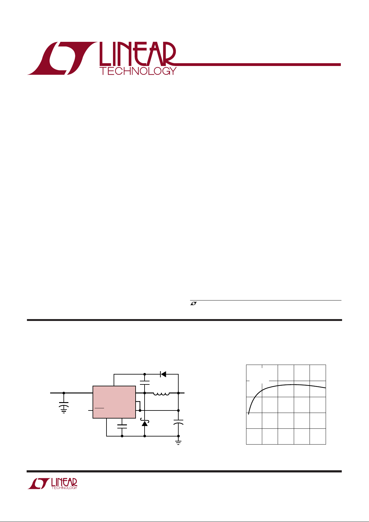
5V Buck Converter
LOAD CURRENT (A)
0
EFFICIENCY (%)
100
90
80
70
60
50
1.00
1375/76 TA02
0.25
0.50
0.75
1.25
V
OUT
= 5V
V
IN
= 10V
L = 10µH
Efficiency vs Load Current
BOOST
LT1376-5
V
IN
OUTPUT**
5V, 1.25A
* RIPPLE CURRENT ≥ I
OUT
/2
** INCREASE L1 TO 10µH FOR LOAD CURRENTS ABOVE 0.6A AND TO 20µH ABOVE 1A
†
FOR INPUT VOLTAGE BELOW 7.5V, SOME RESTRICTIONS MAY APPLY.
SEE APPLICATIONS INFORMATION.
INPUT
6V
†
TO 25V
1375/76 TA01
C2
0.1µF
C
C
3.3nF
D2
1N5818
C1
100µF, 10V
SOLID
TANTALUM
C3*
10µF TO
50µF
D2
1N914
L1**
5µH
V
SW
FB
BIAS
GND
V
C
DEFAULT
= ON
SHDN
+
+
FEATURES
APPLICATIO S
U
DESCRIPTIO
U
TYPICAL APPLICATIO
U
2
LT1375/LT1376
ABSOLUTE MAXIMUM RATINGS
W
WW
U
Input Voltage
LT1375/LT1376.................................................. 25V
LT1375HV/LT1376HV ........................................ 30V
BOOST Pin Voltage
LT1375/LT1376.................................................. 35V
LT1375HV/LT1376HV ........................................ 40V
SHDN Pin Voltage..................................................... 7V
BIAS Pin Voltage ...................................................... 7V
FB Pin Voltage (Adjustable Part)............................ 3.5V
FB Pin Current (Adjustable Part)............................ 1mA
Sense Voltage (Fixed 5V Part) .................................. 7V
SYNC Pin Voltage ..................................................... 7V
Operating Ambient Temperature Range
LT1375C/LT1376C ................................. 0°C to 70°C
LT1375I/LT1376I............................... –40°C to 85°C
Operating Junction Temperature Range
LT1375C/LT1376C ............................... 0°C to 125° C
LT1375I/LT1376I............................. –40°C to 125°C
Storage Temperature Range................ –65° C to 150°C
Lead Temperature (Soldering, 10 sec)................. 300°C
(Note 1)
PACKAGE/ORDER INFORMATION
W
UU
TOP VIEW
S PACKAGE
16-LEAD PLASTIC NARROW SO
1
2
3
4
5
6
7
8
16
15
14
13
12
11
10
9
GND
NC
BOOST
V
IN
V
SW
BIAS
NC
GND
GND
NC
V
C
FB/SENSE
GND
SHDN
NC
GND
ORDER PART NUMBER
θ
JA
=50°C/W WITH FUSED CORNER PINS
CONNECTED TO GROUND PLANE OR LARGE
LANDS
1
2
3
4
8
7
6
5
TOP VIEW
BOOST
V
IN
V
SW
BIAS
N8 PACKAGE
8-LEAD PDIP
S8 PACKAGE
8-LEAD PLASTIC SO
V
C
FB/SENSE
GND
SHDN
θ
JA
= 100°C/W (N8)
θ
JA
= 120°C/W TO 150°C/W DEPENDING ON
PC BOARD LAYOUT (S8)
1
2
3
4
8
7
6
5
TOP VIEW
V
C
FB/SENSE
GND
SYNC
N8 PACKAGE
8-LEAD PDIP
S8 PACKAGE
8-LEAD PLASTIC SO
BOOST
V
IN
V
SW
SHDN
θ
JA
= 100°C/W (N8)
θ
JA
= 120°C/W TO 150°C/W DEPENDING ON
PC BOARD LAYOUT (S8)
LT1375CN8
LT1375CN8-5
LT1375CS8
LT1375CS8-5
LT1375HVCS8
ORDER PART NUMBER
ORDER PART NUMBER
LT1375IN8
LT1375IN8-5
LT1375IS8
LT1375IS8-5
LT1375HVIS8
LT1376CN8
LT1376CN8-5
LT1376CS8
LT1376CS8-5
LT1376HVCS8
LT1376IN8
LT1376IN8-5
LT1376IS8
LT1376IS8-5
LT1376HVIS8
S8 PART MARKING S8 PART MARKING
1375I
1375I5
375HVI
1375
13755
1375HV
1376
13765
1376HV
1376I
1376I5
376HVI
LT1376CS
LT1376IS
LT1376HVCS
LT1376HVIS
Consult factory for Military grade parts.
3
LT1375/LT1376
ELECTRICAL CHARACTERISTICS
The ● denotes specifications which apply over the full operating
temperature range, otherwise specifications are at T
A
= 25°C. T
J
= 25°C, V
IN
= 15V, V
C
= 1.5V, boost open, switch open,
unless otherwise noted.
PARAMETER CONDITIONS MIN TYP MAX UNITS
Reference Voltage (Adjustable) 2.39 2.42 2.45 V
All Conditions
● 2.36 2.48 V
Sense Voltage (Fixed 5V) 4.94 5.0 5.06 V
All Conditions
● 4.90 5.10 V
Sense Pin Resistance 71014 kΩ
Reference Voltage Line Regulation 5V ≤ V
IN
≤ 25V 0.01 0.03 %/V
5V ≤ V
IN
≤ 30V (LT1375HV/LT1376HV) 0.01 0.03 %/V
Feedback Input Bias Current ● 0.5 1.5 µA
Error Amplifier Voltage Gain V
SHDN
= 1V (Notes 2, 8) 200 400
Error Amplifier Transconductance V
SHDN
= 1V, ∆I (V
C
) = ±10µA (Note 8) 1500 2000 2700 µMho
● 1100 3000 µMho
V
C
Pin to Switch Current Transconductance 2A/V
Error Amplifier Source Current V
SHDN
= 1V, V
FB
= 2.1V or V
SENSE
= 4.4V ● 150 225 320 µA
Error Amplifier Sink Current V
SHDN
= 1V, V
FB
= 2.7V or V
SENSE
= 5.6V 2 mA
V
C
Pin Switching Threshold Duty Cycle = 0 0.9 V
V
C
Pin High Clamp V
SHDN
= 1V 2.1 V
Switch Current Limit V
C
Open, V
FB
= 2.1V or V
SENSE
= 4.4V,
V
BOOST
= V
IN
+ 5V DC ≤ 50% ● 1.50 2 3 A
DC = 80%
● 1.35 3 A
Switch On Resistance (Note 6) I
SW
= 1.5A, V
BOOST
= V
IN
+ 5V 0.3 0.4 Ω
● 0.5 Ω
Maximum Switch Duty Cycle V
FB
= 2.1V or V
SENSE
= 4.4V 90 93 %
–40°C ≤ T
J
≤ 125°C8693 %
T
J
= 150°C8593 %
Switch Frequency V
C
Set to Give 50% Duty Cycle 460 500 540 kHz
–25°C ≤ T
J
≤ 125°C 440 560 kHz
T
J
≤ –25°C 440 570 kHz
Switch Frequency Line Regulation 5V
≤ V
IN
≤ 25V ● 0.05 0.15 %/V
5V ≤ V
IN
≤ 30V (LT1375HV/LT1376HV) ● 0.05 0.15 %/V
Frequency Shifting Threshold on FB Pin ∆f = 10kHz ● 0.8 1.0 1.3 V
Minimum Input Voltage (Note 3) ● 5.0 5.5 V
Minimum Boost Voltage (Note 4) I
SW
≤ 1.5A ● 3 3.5 V
Boost Current (Note 5) V
BOOST
= V
IN
+ 5V I
SW
= 500mA ● 12 22 mA
I
SW
= 1.5A ● 25 35 mA
Input Supply Current (Note 6) V
BIAS
= 5V ● 0.9 1.4 mA
Output Supply Current (Note 6) V
BIAS
= 5V ● 3.2 4.0 mA
Shutdown Supply Current V
SHDN
= 0V, V
IN
≤ 25V, V
SW
= 0V, V
C
Open 15 50 µA
● 75 µA
V
SHDN
= 0V, V
IN
≤ 30V, V
SW
= 0V, V
C
Open
(LT1375HV/LT1376HV) 20 75 µA
● 100 µA
Lockout Threshold V
C
Open ● 2.3 2.38 2.46 V
4
LT1375/LT1376
Kool Mµ is a registered trademark of Magnetics, Inc.
ELECTRICAL CHARACTERISTICS
Note 1: Absolute Maximum Ratings are those values beyond which the life
of a device may be impaired.
Note 2: Gain is measured with a V
C
swing equal to 200mV above the low
clamp level to 200mV below the upper clamp level.
Note 3: Minimum input voltage is not measured directly, but is guaranteed
by other tests. It is defined as the voltage where internal bias lines are still
regulated so that the reference voltage and oscillator frequency remain
constant. Actual minimum input voltage to maintain a regulated output will
depend on output voltage and load current. See Applications Information.
Note 4: This is the minimum voltage across the boost capacitor needed to
guarantee full saturation of the internal power switch.
Note 5: Boost current is the current flowing into the BOOST pin with the
pin held 5V above input voltage. It flows only during switch-on time.
Note 6: Input supply current is the bias current drawn by the input pin
when the BIAS pin is held at 5V with switching disabled. Output supply
current is the current drawn by the BIAS pin when the bias pin is held at
5V. Total input referred supply current is calculated by summing input
supply current (I
SI
) with a fraction of output supply current (I
SO
):
I
TOT
= I
SI
+ (I
SO
)(V
OUT
/V
IN
)(1.15)
With V
IN
= 15V, V
OUT
= 5V, I
SI
= 0.9mA, I
SO
= 3.6mA, I
TOT
= 2.28mA.
For the LT1375, quiescent current is equal to:
I
TOT
= I
SI
+ I
SO
(1.15)
because the BIAS pin is internally connected to V
IN
.
Note 7: Switch-on resistance is calculated by dividing V
IN
to V
SW
voltage
by the forced current (1.5A). See Typical Performance Characteristics for
the graph of switch voltage at other currents.
Note 8: Transconductance and voltage gain refer to the internal amplifier
exclusive of the voltage divider. To calculate gain and transconductance
refer to sense pin on fixed voltage parts. Divide values shown by the ratio
V
OUT
/2.42.
The ● denotes specifications which apply over the full operating
temperature range, otherwise specifications are at T
A
= 25°C. T
J
= 25°C, V
IN
= 15V, V
C
= 1.5V, boost open, switch open,
unless otherwise noted.
PARAMETER CONDITIONS MIN TYP MAX UNITS
Shutdown Thresholds V
C
Open Device Shutting Down ● 0.15 0.37 0.60 V
Device Starting Up
● 0.25 0.45 0.60 V
V
C
Open LT1375HV/LT1376HV Device Shutting Down ● 0.15 0.37 0.70 V
LT1375HV/LT1376HV Device Starting Up
● 0.25 0.45 0.70 V
Minimum Synchronizing Amplitude (LT1375 Only) V
IN
= 5V ● 1.5 2.2 V
Synchronizing Range (LT1375 Only) 580 900 kHz
SYNC Pin Input Resistance 40 kΩ
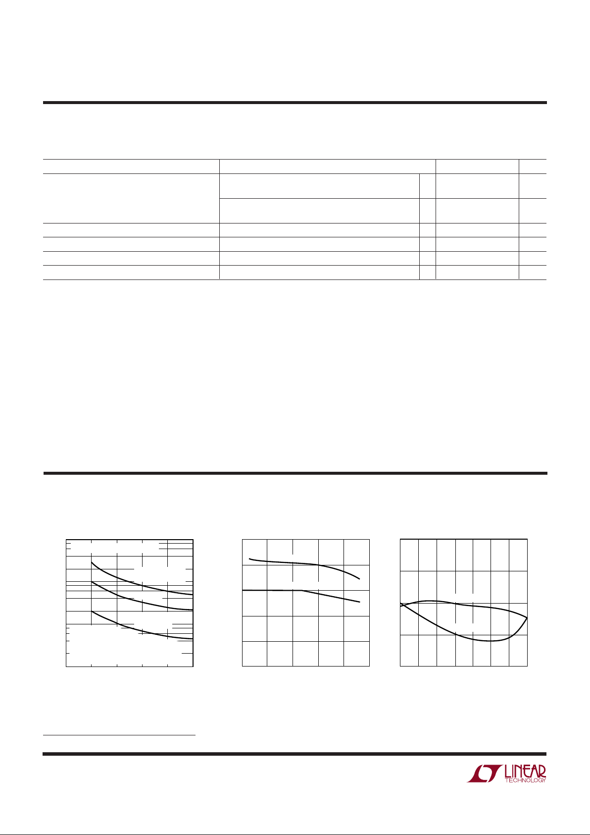
INDUCTANCE (µH)
05
CORE LOSS (W)
CORE LOSS (% OF 5W LOAD)
1.0
0.1
0.01
0.001
10 15 20
20
12
8
4
2
1.2
0.8
0.4
0.2
0.12
0.08
0.04
0.02
25
1375/76 G01
TYPE 52
POWDERED IRON
Kool Mµ
®
PERMALLOY
µ = 125
V
OUT
= 5V, V
IN
= 10V, I
OUT
= 1A
CORE LOSS IS
INDEPENDENT OF LOAD
CURRENT UNTIL LOAD CURRENT FALLS
LOW ENOUGH FOR CIRCUIT TO GO INTO
DISCONTINUOUS MODE
Inductor Core Loss
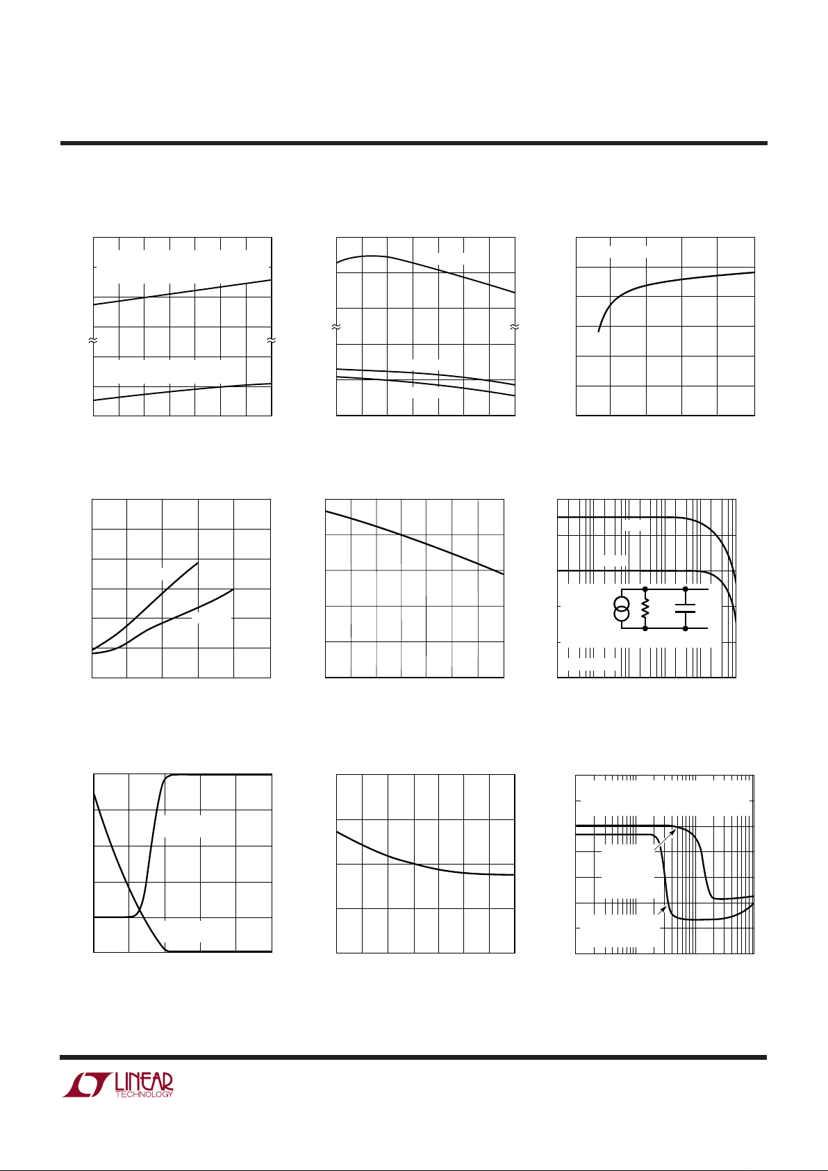
TYPICAL PERFORMANCE CHAR ACTERISTICS
UW
DUTY CYCLE (%)
0
SWITCH PEAK CURRENT (A)
2.5
2.0
1.5
1.0
0.5
0
80
1375/76 G08
20
40
60
100
TYPICAL
GUARANTEED MINIMUM
Switch Peak Current Limit
JUNCTION TEMPERATURE (°C)
–50
2.44
2.43
2.42
2.41
2.40
100
1375/76 G09
–25 0 25 50 75 125
FEEDBACK VOLTAGE (V)
CURRENT (µA)
2.0
1.5
1.0
0.5
0
VOLTAGE
CURRENT
Feedback Pin Voltage and Current
5
LT1375/LT1376
TYPICAL PERFORMANCE CHAR ACTERISTICS
UW
TEMPERATURE (°C)
–50
500
400
300
200
8
4
0
25 75
1375/76 G04
–25 0
50 100 125
CURRENT (µA)
CURRENT REQUIRED TO FORCE SHUTDOWN
(FLOWS OUT OF PIN). AFTER SHUTDOWN,
CURRENT DROPS TO A FEW µA
AT 2.38V STANDBY THRESHOLD
(CURRENT FLOWS OUT OF PIN)
Shutdown Pin Bias Current
JUNCTION TEMPERATURE (°C)
–50
TRANSCONDUCTANCE (µMho)
2500
2000
1500
1000
500
0
0
50
75
1375/76 G02
–25
25
100
125
Error Amplifier Transconductance
FREQUENCY (Hz)
GAIN (µMho)
PHASE (DEG)
3000
2500
2000
1500
1000
500
200
150
100
50
0
–50
100 10k 100k 10M
1375/76 G03
1k 1M
GAIN
PHASE
ERROR AMPLIFIER EQUIVALENT CIRCUIT
R
OUT
200k
C
OUT
12pF
V
C
R
LOAD
= 50Ω
V
FB
2 • 10
–3
)(
Error Amplifier Transconductance
Frequency Foldback
LOAD CURRENT (mA)
0
INPUT VOLTAGE (V)
8.5
8.0
7.5
7.0
6.5
6.0
5.5
5.0
10 100 1000
1375/76 G12
MINIMUM INPUT VOLTAGE CAN BE
REDUCED BY ADDING A SMALL EXTERNAL
PNP. SEE APPLICATIONS INFORMATION
MINIMUM
VOLTAGE TO
START WITH
STANDARD
CIRCUIT
MINIMUM VOLTAGE
TO RUN WITH
STANDARD CIRCUIT
LT1376 Minimum Input Voltage
with 5V Output
Shutdown Supply Current
INPUT VOLTAGE (V)
0
INPUT SUPPLY CURRENT (µA)
30
25
20
15
10
5
0
5101520
1375/76 G06
25
V
SHUTDOWN
= 0V
JUNCTION TEMPERATURE (°C)
–50
2.40
2.36
2.32
0.8
0.4
0
25 75
1375/76 G05
–25 0
50 100 125
SHUTDOWN PIN VOLTAGE (V)
STANDBY
START-UP
SHUTDOWN
Standby and Shutdown Thresholds
Shutdown Supply Current
SHUTDOWN VOLTAGE (V)
0
INPUT SUPPLY CURRENT (µA)
150
125
100
75
50
25
0
0.1 0.2 0.3 0.4
1375/76 G07
0.5
V
IN
= 25V
V
IN
= 10V
FEEDBACK PIN VOLTAGE (V)
0
SWITCHING FREQUENCY (kHz) OR CURRENT (µA)
500
400
300
200
100
0
2.0
1375/76 G10
0.5
1.0
1.5
2.5
SWITCHING
FREQUENCY
FEEDBACK PIN
CURRENT
Switching Frequency
JUNCTION TEMPERATURE (°C)
–50
600
550
500
450
400
100
1375/76 G11
–25 0 25 50 75 125
FREQUENCY (kHz)
6
LT1375/LT1376
TYPICAL PERFORMANCE CHARACTERISTICS
U
W
INPUT VOLTAGE (V)
0
CURRENT (A)
1.50
1.25
1.00
0.75
0.50
0.25
0
5101520
1375/76 G13
25
L = 20µH
L = 10µH
L = 5µH
V
OUT
= 10V
INPUT VOLTAGE (V)
0
CURRENT (A)
1.50
1.25
1.00
0.75
0.50
0.25
0
5101520
1375/76 G14
25
L = 20µH
L = 10µH
L = 5µH
V
OUT
= 3.3V
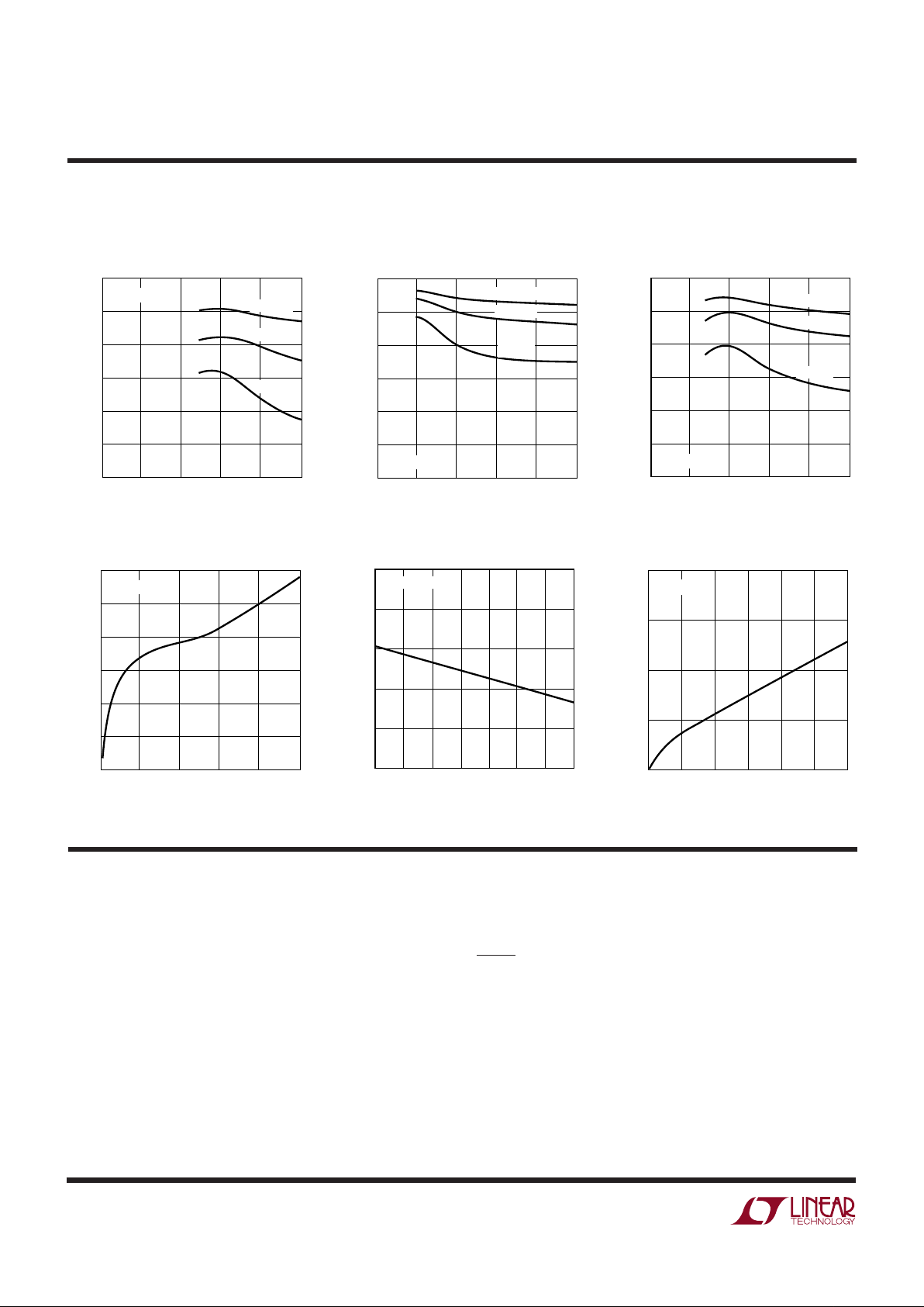
Maximum Load Current
at V
OUT
= 10V
Maximum Load Current
at V
OUT
= 3.3V
Maximum Load Current
at V
OUT
= 5V
INPUT VOLTAGE (V)
0
CURRENT (A)
1.50
1.25
1.00
0.75
0.50
0.25
0
5101520
1375/76 G15
25
L = 20µH
L = 10µH
L = 5µH
V
OUT
= 5V
PIN FUNCTIONS
UUU
BOOST: The BOOST pin is used to provide a drive voltage,
higher than the input voltage, to the internal bipolar NPN
power switch. Without this added voltage, the typical
switch voltage loss would be about 1.5V. The additional
boost voltage allows the switch to saturate and voltage
loss approximates that of a 0.3Ω FET structure, but with
much smaller die area. Efficiency improves from 75% for
conventional bipolar designs to > 87% for these new parts.
V
SW
: The switch pin is the emitter of the on-chip power
NPN switch. It is driven up to the input pin voltage during
switch on time. Inductor current drives the switch pin
negative during switch off time. Negative voltage is clamped
with the external catch diode. Maximum negative switch
voltage allowed is –0.8V.
SHDN: The shutdown pin is used to turn off the regulator
and to reduce input drain current to a few microamperes.
Actually, this pin has two separate thresholds, one at
2.38V to disable switching, and a second at 0.4V to force
complete micropower shutdown. The 2.38V threshold
functions as an accurate undervoltage lockout (UVLO).
This is sometimes used to prevent the regulator from
operating until the input voltage has reached a predeter-
mined level.
SWITCH CURRENT (A)
0
BOOST PIN CURRENT (mA)
12
10
8
6
4
2
0
0.25 0.50 0.75 1.00
1375/76 G16
1.25
T
J
= 25°C
BOOST Pin Current
V
C
Pin Shutdown Threshold
SWITCH CURRENT (A)
0
SWITCH VOLTAGE (V)
0.8
0.6
0.4
0.2
0
0.25 0.50 0.75 1.00
1375/76 G18
1.25 1.50
T
J
= 25°C
Switch Voltage Drop
JUNCTION TEMPERATURE (°C)
–50
1.4
1.2
1.0
0.8
0.6
0.4
100
1375/76 G11
–25 0 25 50 75 125
THRESHOLD VOLTAGE (V)
SHUTDOWN

7
LT1375/LT1376
PIN FUNCTIONS
UUU
BIAS (LT1376 Only): The BIAS pin is used to improve
efficiency when operating at higher input voltages and
light load current. Connecting this pin to the regulated
output voltage forces most of the internal circuitry to draw
its operating current from the output voltage rather than
the input supply. This is a much more efficient way of
doing business if the input voltage is much higher than the
output.
Minimum output voltage setting for this mode of
operation is 3.3V
. Efficiency improvement at V
IN
= 20V,
V
OUT
= 5V, and I
OUT
= 25mA is over 10%.
SYNC (LT1375 Only): The SYNC pin is used to synchro-
nize the internal oscillator to an external signal. It is directly
logic compatible and can be driven with any signal be-
tween 10% and 90% duty cycle. The synchronizing range
is equal to
initial
operating frequency, up to 900kHz. See
Synchronizing section in Applications Information for
details.
FB/SENSE: The feedback pin is used to set output voltage,
using an external voltage divider that generates 2.42V at
the pin with the desired output voltage. The fixed voltage
(-5) parts have the divider included on the chip, and the FB
pin is used as a SENSE pin, connected directly to the 5V
output. Two additional functions are performed by the FB
pin. When the pin voltage drops below 1.7V, switch
current limit is reduced. Below 1V, switching frequency is
also reduced. See Feedback Pin Function section in Appli-
cations Information for details.
V
C
: The V
C
pin is the output of the error amplifier and the
input of the peak switch current comparator. It is normally
used for frequency compensation, but can do double duty
as a current clamp or control loop override. This pin sits
at about 1V for very light loads and 2V at maximum load.
It can be driven to ground to shut off the regulator, but if
driven high, current must be limited to 4mA.
GND: The GND pin connection needs consideration for
two reasons. First, it acts as the reference for the regulated
output, so load regulation will suffer if the “ground” end of
the load is not at the same voltage as the GND pin of the
IC. This condition will occur when load current or other
currents flow through metal paths between the GND pin
and the load ground point. Keep the ground path short
between the GND pin and the load, and use a ground plane
when possible. The second consideration is EMI caused
by GND pin current spikes. Internal capacitance between
the V
SW
pin and the GND pin creates very narrow (<10ns)
current spikes in the GND pin. If the GND pin is connected
to system ground with a long metal trace, this trace may
radiate excess EMI. Keep the path between the input
bypass and the GND pin short.
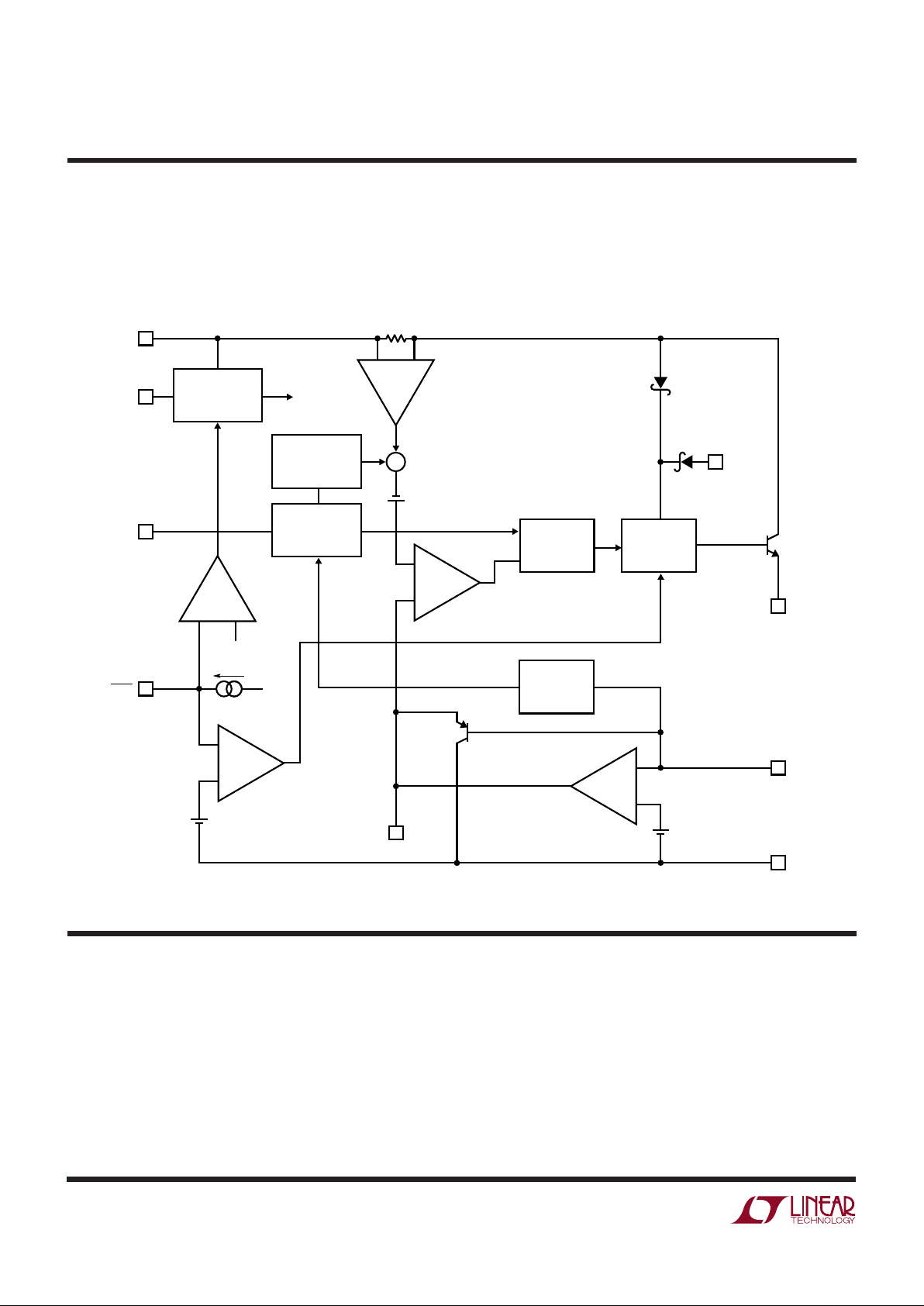
BLOCK DIAGRAM
W
The LT1376 is a constant frequency, current mode buck
converter. This means that there is an internal clock and
two feedback loops that control the duty cycle of the power
switch. In addition to the normal error amplifier, there is a
current sense amplifier that monitors switch current on a
cycle-by-cycle basis. A switch cycle starts with an oscilla-
tor pulse which sets the R
S
flip-flop to turn the switch on.
When switch current reaches a level set by the inverting
input of the comparator, the flip-flop is reset and the
switch turns off. Output voltage control is obtained by
using the output of the error amplifier to set the switch
current trip point. This technique means that the error
amplifier commands current to be delivered to the output
rather than voltage. A voltage fed system will have low
phase shift up to the resonant frequency of the inductor
and output capacitor, then an abrupt 180° shift will occur.
The current fed system will have 90° phase shift at a much
lower frequency, but will not have the additional 90° shift
until well beyond the LC resonant frequency. This makes
it much easier to frequency compensate the feedback loop
and also gives much quicker transient response.
Most of the circuitry of the LT1376 operates from an
internal 2.9V bias line. The bias regulator normally draws
power from the regulator input pin, but if the BIAS pin is
connected to an external voltage higher than 3V, bias
power will be drawn from the external source (typically the
regulated output voltage). This will improve efficiency if
the BIAS pin voltage is lower than regulator input voltage.
8
LT1375/LT1376
High switch efficiency is attained by using the BOOST pin
to provide a voltage to the switch driver which is higher
than the input voltage, allowing switch to be saturated.
This boosted voltage is generated with an external capaci-
BLOCK DIAGRAM
W
tor and diode. Two comparators are connected to the
shutdown pin. One has a 2.38V threshold for undervoltage
lockout and the second has a 0.4V threshold for complete
shutdown.
–
+
–
+
–
+
–
+
Σ
INPUT
2.9V BIAS
REGULATOR
500kHz
OSCILLATOR
FREQUENCY
SHIFT CIRCUIT
V
SW
FB
V
C
GND
1375/76 BD
SLOPE COMP
0.1Ω
BIAS
INTERNAL
V
CC
CURRENT
SENSE
AMPLIFIER
VOLTAGE GAIN = 10
SYNC
SHUTDOWN
COMPARATOR
CURRENT
COMPARATOR
ERROR
AMPLIFIER
g
m
= 2000µMho
FOLDBACK
CURRENT
LIMIT
CLAMP
BOOST
R
S
FLIP-FLOP
DRIVER
CIRCUITRY
S
R
0.9V
LOCKOUT
COMPARATOR
0.4V
3.5µA
Q2
Q1
POWER
SWITCH
2.38V
2.42V
–
+
SHDN
Figure 1. Block Diagram
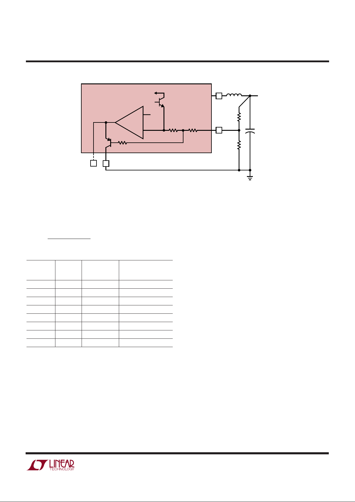
APPLICATIONS INFORMATION
WUU
U
FEEDBACK PIN FUNCTIONS
The feedback (FB) pin on the LT1376 is used to set output
voltage and also to provide several overload protection
features. The first part of this section deals with selecting
resistors to set output voltage and the remaining part talks
about foldback frequency and current limiting created by
the FB pin. Please read both parts before committing to a
final design. The fixed 5V LT1376-5 has internal divider
resistors and the FB pin is renamed SENSE, connected
directly to the output.
The suggested value for the output divider resistor (see
Figure 2) from FB to ground (R2) is 5k or less, and a
formula for R1 is shown below. The output voltage error
caused by ignoring the input bias current on the FB pin is
less than 0.25% with R2 = 5k. A table of standard 1%
values is shown in Table 1 for common output voltages.
9
LT1375/LT1376
APPLICATIONS INFORMATION
WUU
U
–
+
2.4V
V
SW
V
C
GND
1375/76 F02
TO FREQUENCY
SHIFTING
R3
1k
R4
1k
R1
R2
5k
OUTPUT
5V
R5
5k
ERROR
AMPLIFIER
FB
1.6V
Q1
LT1375/LT1376
Q2
+
Figure 2. Frequency and Current Limit Foldback
Please read the following if divider resistors are increased
above the suggested values.
R
RV
OUT
1
2242
242
=
−
()
.
.
Table 1
OUTPUT R1 % ERROR AT OUTPUT
VOLTAGE R2 (NEAREST 1%) DUE TO DISCREET 1%
(V) (k
Ω
)(k
Ω
) RESISTOR STEPS
3 4.99 1.21 +0.23
3.3 4.99 1.82 +0.08
5 4.99 5.36 +0.39
6 4.99 7.32 –0.5
8 4.99 11.5 –0.04
10 4.99 15.8 +0.83
12 4.99 19.6 –0.62
15 4.99 26.1 +0.52
More Than Just Voltage Feedback
The feedback (FB) pin is used for more than just output
voltage sensing. It also reduces switching frequency and
current limit when output voltage is very low (see the
Frequency Foldback graph in Typical Performance Char-
acteristics). This is done to control power dissipation in
both the IC and in the external diode and inductor during
short-circuit conditions. A shorted output requires the
switching regulator to operate at very low duty cycles, and
the average current through the diode and inductor is
equal to the short-circuit current limit of the switch (typi-
cally 2A for the LT1376, folding back to less than 1A).
Minimum switch on time limitations would prevent the
switcher from attaining a sufficiently low duty cycle if
switching frequency were maintained at 500kHz, so fre-
quency is reduced by about 5:1 when the feedback pin
voltage drops below 1V (see Frequency Foldback graph).
This does not affect operation with normal load condi-
tions; one simply sees a gear shift in switching frequency
during start-up as the output voltage rises.
In addition to lower switching frequency, the LT1376 also
operates at lower switch current limit when the feedback
pin voltage drops below 1.7V. Q2 in Figure 2 performs this
function by clamping the V
C
pin to a voltage less than its
normal 2.3V upper clamp level. This
foldback current limit
greatly reduces power dissipation in the IC, diode and
inductor during short-circuit conditions. Again, it is nearly
transparent to the user under normal load conditions. The
only loads which may be affected are current source loads
which maintain full load current with output voltage less
than 50% of final value. In these rare situations the
Feedback pin can be clamped above 1.5V with an external
diode to defeat foldback current limit.
Caution:
clamping
the feedback pin means that frequency shifting will also be
defeated, so a combination of high input voltage and dead
shorted output may cause the LT1376 to lose control of
current limit.
The internal circuitry which forces reduced switching
frequency also causes current to flow out of the feedback
 Loading...