


Linear Technology LTC1148CS-5, LTC1148CS-3.3, LTC1148CS, LTC1148CN-5, LTC1148CN-3.3 Datasheet
...LTC1148
LTC1148-3.3/LTC1148-5
High Efficiency Synchronous
Step-Down Switching Regulators
FEATURES
■Ultrahigh Efficiency: Over 95% Possible
■Current-Mode Operation for Excellent Line and Load Transient Response
■High Efficiency Maintained Over Three Decades of Output Current
■Low 160μA Standby Current at Light Loads
■Logic Controlled Micropower Shutdown: IQ < 20μA
■Wide VIN Range: 3.5V* to 20V
■Short-Circuit Protection
■Very Low Dropout Operation: 100% Duty Cycle
■Synchronous FET Switching for High Efficiency
■Adaptive Nonoverlap Gate Drives
■Output Can Be Externally Held High in Shutdown
■Available in 14-Pin Narrow SO Package
APPLICATIOUS
■Notebook and Palmtop Computers
■Portable Instruments
■Battery-Operated Digital Devices
■Cellular Telephones
■DC Power Distribution Systems
■GPS Systems
DESCRIPTIOU
The LTC®1148 series is a family of synchronous stepdown switching regulator controllers featuring automatic Burst ModeTM operation to maintain high efficiencies at low output currents. These devices drive external complementary power MOSFETs at switching frequencies up to 250kHz using a constant off-time current-mode architecture providing constant ripple current in the inductor.
The operating current level is user-programmable via an external current sense resistor. Wide input supply range allows operation from 3.5V* to 18V (20V maximum). Constant off-time architecture provides low dropout regu-
lation limited by only the RDS(ON) of the external MOSFET and resistance of the inductor and current sense resistor.
The LTC1148 series combines synchronous switching for maximum efficiency at high currents with an automatic low currentoperatingmode,calledBurstModeoperation,which reduces switching losses. Standby power is reduced to only
2mW at VIN = 10V (at IOUT = 0). Load currents in Burst Mode operation are typically 0mA to 300mA.
For operation up to 48V input, see the LTC1149 and LTC1159 data sheets and Application Note 54.
, LTC and LT are registered trademarks of Linear Technology Corporation.
Burst Mode is a trademark of Linear Technology Corporation. * LTC1148L and LTC1148L-3.3 only.
TYPICAL APPLICATIOU
|
|
|
|
|
|
|
|
|
|
|
VIN (5.2V TO 18V) |
|
|
|
|
|
|
|
|
|
|
|
|
|
|
||
+ |
|
|
|
1μF |
|
|
|
|
|
|
|
|
|
|
|
|
+ |
|
|
|
CIN |
|
|||||
|
|
|
|
|
|
|
|
|
|
|
|
|
|
|
|
|
|
|
|
|
|
|
|
|
|
||
|
|
|
|
|
|
|
|
|
VIN |
|
|
|
|
|
|
|
|
|
|
|
|
100μF |
|
||||
|
|
|
|
|
|
|
|
|
|
|
|
|
|
|
|
|
|
|
|
|
|
|
|||||
|
|
|
|
|
|
|
|
|
|
|
P-DRIVE |
|
|
|
|
|
|
P-CHANNEL |
L* |
|
|
|
|
|
RSENSE** |
|
|
|
|
|
|
|
|
|
|
|
|
|
|
|
|
|
|
|
Si4431DY |
|
|
|
|
|
|
||||
0V = NORMAL |
|
|
LTC1148HV-5 |
|
|
|
|
|
62μH |
|
|
|
|
|
|
0.05Ω |
VOUT |
||||||||||
|
|
SHUTDOWN |
|
|
|
|
|
|
|
|
|
|
|
|
|
||||||||||||
>1.5V = SHUTDOWN |
|
|
|
|
|
|
|
|
|
|
|
|
|
|
|
5V/2A |
|||||||||||
|
|
|
SENSE+ |
|
|
|
|
|
|
|
|
|
|
|
|
|
|
|
|
||||||||
|
|
|
|
|
|
|
|
|
|
|
|
|
|
|
|
|
|
|
|
|
|
|
|
|
|
|
|
|
|
ITH |
SENSE– |
1000pF |
+ |
|
RC |
|
CT |
|
COUT |
||
|
|
N-CHANNEL |
||||
|
|
N-DRIVE |
D1 |
|||
1k |
CT |
|
Si4412DY |
MBRS140T3 |
390μF |
|
|
SGND |
PGND |
|
|||
CC |
470pF |
|
|
|
||
|
|
|
|
|
||
3300pF |
|
|
|
|
|
LT1148 • TA01 |
|
|
|
|
|
*COILTRONICS CTX62-2-MP |
|
|
|
|
|
|
**KRL SL-1-C1-0R050J |
|
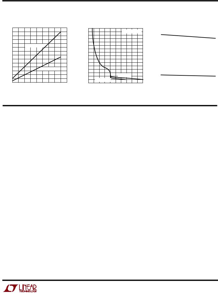
Figure 1. High Efficiency Step-Down Converter
|
|
|
LTC1148-5 Efficiency |
|
|
||||||||||||||||||
|
100 |
|
|
|
|
|
|
|
|
|
|
|
|
|
|
|
|
|
|
|
|
|
|
|
|
|
|
|
|
|
|
|
|
|
|
|
|
|
|
|
|
|
|
|
|
|
|
|
|
|
|
|
|
|
|
|
VIN = 6V |
|
|
|
|
|
|
|
|
|
|||||
|
95 |
|
|
|
|
|
|
|
|
|
|
|
|
|
|
|
|
|
|
|
|
|
|
(%) |
|
|
V |
IN |
|
= 10V |
|
|
|||||||||||||||
|
|
|
|
|
|
|
|
|
|
|
|
|
|
|
|
|
|
||||||
|
|
|
|
|
|
|
|
|
|
|
|
|
|
|
|
|
|
|
|
|
|
|
|
|
|
|
|
|
|
|
|
|
|
|
|
|
|
|
|
|
|
|
|
|
|
|
|
EFFICIENCY |
90 |
|
|
|
|
|
|
|
|
|
|
|
|
|
|
|
|
|
|
|
|
|
|
|
|
|
|
|
|
|
|
|
|
|
|
|
|
|
|
|
|
|
|
|
|
|
|
|
85 |
|
|
|
|
|
|
|
|
|
|
|
|
|
|
|
|
|
|
|
|
|
|
|
|
|
|
|
|
|
|
|
|
|
|
|
|
|
|
|
|
|
|
|
|
|
|
|
|
|
|
|
|
|
|
|
|
|
|
|
|
|
|
|
|
|
|
|
|
|
|
|
80 |
|
|
|
|
|
|
|
|
|
|
|
|
|
|
|
|
|
|
|
|
|
|
|
|
|
|
|
|
|
|
|
|
|
|
|
|
|
|
|
|
|
|
|
|
|
|
|
|
0.2 |
|
|
|
|
|
|
|
|
|
2 |
|||||||||||
|
0.02 |
|
|
|
|
|
|
|
|
|
|||||||||||||
LOAD CURRENT (A)
LTC1148 • TA01
1

LTC1148 LTC1148-3.3/LTC1148-5
ABSOLUTE WAXIWUW RATIUGS
(Note 1)
Input Supply Voltage (Pin 3) |
|
|
LTC1148 and LTC1148L Series |
............ |
16V to – 0.3V |
LTC1148HV Series ............................... |
|
20V to – 0.3V |
Continuous Output Current (Pins 1, ..............14) |
50mA |
|
Sense Voltages (Pins 7, 8) |
|
|
LTC1148HV (Adjustable Only) |
|
|
VIN ³ 12.7V ...................................... |
|
13V to – 0.3V |
VIN < 12.7V ......................... |
(V IN + 0.3V) to – 0.3V |
|
Operating Ambient Temperature Range ...... |
0°C to 70°C |
|
Extended Commercial |
|
– 40°C to 85°C |
Temperature Range ............................... |
|
|
Junction Temperature (Note 2) ............................ |
|
125°C |
Storage Temperature Range ................ |
|
– 65°C to 150°C |
Lead Temperature (Soldering, 10 sec)................. |
300°C |
|
PACKAGE/ORDER IUFORWATIOU
|
|
|
|
|
|
ORDER PART |
|
|
|
|
|
|
|
NUMBER |
|
|
|
|
TOP VIEW |
|
|
||
|
|
|
|
LTC1148CN |
|||
|
|
|
|
|
|
||
|
|
|
|
|
|
||
P-DRIVE |
1 |
|
|
14 |
N-DRIVE |
LTC1148HVCN |
|
|
|
|
|
|
|
||
NC |
2 |
|
|
13 |
NC |
LTC1148CN-3.3 |
|
|
|
|
|
|
|
||
VIN |
3 |
|
|
12 |
PGND |
||
|
|
LTC1148HVCN-3.3 |
|||||
|
|
|
|
|
|
||
CT |
4 |
|
|
11 |
SGND |
||
|
|
LTC1148CN-5 |
|||||
|
|
|
|
|
|
||
INTVCC |
5 |
|
|
10 |
SHUTDOWN |
||
|
|
LTC1148HVCN-5 |
|||||
|
|
|
|
|
|
||
ITH |
6 |
|
|
9 |
VFB* |
||
|
|
LTC1148CS |
|||||
|
|
|
|
||||
SENSE– |
7 |
|
|
8 |
SENSE+ |
||
|
|
|
|
|
|
LTC1148HVCS |
|
N PACKAGE |
S PACKAGE |
||||||
LTC1148LCS |
|||||||
14-LEAD PDIP |
14-LEAD PLASTIC SO |
||||||
*FIXED OUTPUT VERSIONS = NC |
LTC1148CS-3.3 |
||||||
TJMAX = 125°C, θJA = 70°C/ W (N) |
LTC1148HVCS-3.3 |
||||||
TJMAX = 125°C, θJA = 110°C/ W (S) |
LTC1148LCS-3.3 |
||||||
|
|
|
|
|
|
LTC1148CS-5 |
|
|
|
|
|
|
|
LTC1148HVCS-5 |
|
|
|
|
|
|
|
|
|
Consult factory for Industrial and Military grade parts.
ELECTRICAL CHARACTERISTICS TA = 25°C, VIN = 10V, VSHUTDOWN = 0V unless otherwise noted.
SYMBOL |
PARAMETER |
CONDITIONS |
|
MIN |
TYP |
MAX |
UNITS |
|
|
|
|
|
|
|
|
V9 |
Feedback Voltage (LTC1148, LTC1148L, |
VIN = 9V |
● |
1.21 |
1.25 |
1.29 |
V |
|
LTC1148HV) |
|
|
|
|
|
|
I9 |
Feedback Current (LTC1148, LTC1148L, |
|
● |
|
0.2 |
1 |
μA |
|
LTC1148HV) |
|
|
|
|
|
|
VOUT |
Regulated Output Voltage |
VIN = 9V |
|
|
|
|
|
|
LTC1148-3.3, LTC1148HV-3.3, LTC1148L-3.3 |
ILOAD = 700mA |
● |
3.23 |
3.33 |
3.43 |
V |
|
LTC1148-5, LTC1148HV-5 |
ILOAD = 700mA |
● |
4.90 |
5.05 |
5.20 |
V |
VOUT |
Output Voltage Line Regulation |
VIN = 7V to 12V, ILOAD = 50mA |
|
– 40 |
0 |
40 |
mV |
|
Output Voltage Load Regulation |
5mA < ILOAD < 2A |
|
|
40 |
65 |
mV |
|
LTC1148-3.3, LTC1148HV-3.3, LTC1148L-3.3 |
● |
|
||||
|
LTC1148-5, LTC1148HV-5 |
5mA < ILOAD < 2A |
● |
|
60 |
100 |
mV |
|
Output Ripple (Burst Mode) |
ILOAD = 0A |
|
|
50 |
|
mVP-P |
IQ |
Input DC Supply Current (Note 3) |
(Note 7) |
|
|
|
|
|
|
LTC1148 Series |
4V < VIN < 12V |
|
|
1.6 |
2.1 |
mA |
|
Normal Mode |
|
|
||||
|
Sleep Mode |
4V < VIN < 12V |
|
|
160 |
230 |
μA |
|
Sleep Mode (LTC1148-5) |
6V < VIN < 12V |
|
|
160 |
230 |
μA |
|
Shutdown |
VSHUTDOWN = 2.1V, 4V < VIN < 12V |
|
|
10 |
20 |
μA |
|
LTC1148HV Series |
4V < VIN < 18V |
|
|
1.6 |
2.3 |
mA |
|
Normal Mode |
|
|
||||
|
Sleep Mode |
4V < VIN < 18V |
|
|
160 |
250 |
μA |
|
Sleep Mode (LTC1148HV-5) |
6V < VIN < 18V |
|
|
160 |
250 |
μA |
|
Shutdown |
VSHUTDOWN = 2.1V, 4V < VIN < 18V |
|
|
10 |
22 |
μA |
|
LTC1148L Series |
3.5V < VIN < 12V |
|
|
1.6 |
2.1 |
mA |
|
Normal Mode |
|
|
||||
|
Sleep Mode |
3.5V < VIN < 12V |
|
|
160 |
230 |
μA |
|
Shutdown |
VSHUTDOWN = 2.1V, 3.5V < VIN < 12V |
|
|
10 |
20 |
μA |
|
|
|
|
|
|
|
|
|
|
|
|
|
|
|
|
2

LTC1148
LTC1148-3.3/LTC1148-5
ELECTRICAL CHARACTERISTICS TA = 25°C, VIN = 10V, VSHUTDOWN = 0V, unless otherwise noted.
SYMBOL |
PARAMETER |
CONDITIONS |
|
|
|
|
|
|
MIN |
TYP |
MAX |
UNITS |
||
|
|
|
|
|
|
|
|
|
|
|
|
|
|
|
V8 – V7 |
Current Sense Threshold Voltage |
|
– = 5V, V |
= V |
|
/4 + 25mV (Forced) |
|
|
25 |
|
mV |
|||
|
|
LTC1148, LTC1148HV, LTC1148L |
V |
|
|
|
|
|||||||
|
|
|
SENSE |
9 |
|
OUT |
|
|
|
|
|
|
|
|
|
|
|
V |
– = 5V, V |
= V |
|
/4 – 25mV (Forced) |
● |
130 |
150 |
170 |
mV |
||
|
|
|
SENSE |
9 |
|
OUT |
|
|
|
|
|
|
|
|
|
|
LTC1148-3.3, LTC1148HV-3.3 |
V |
– = V + 100mV (Forced) |
|
|
25 |
|
mV |
|||||
|
|
|
SENSE |
OUT |
|
|
|
|
|
|
|
|
|
|
|
|
LTC1148L-3.3 |
V |
– = V – 100mV (Forced) |
● |
130 |
150 |
170 |
mV |
|||||
|
|
|
SENSE |
OUT |
|
|
|
|
|
|
|
|
|
|
|
|
LTC1148-5, LTC1148HV-5 |
V |
– = V + 100mV (Forced) |
|
|
25 |
|
mV |
|||||
|
|
|
SENSE |
OUT |
|
|
|
|
|
|
|
|
|
|
|
|
|
V |
– = V – 100mV (Forced) |
● |
130 |
150 |
170 |
mV |
|||||
|
|
|
SENSE |
OUT |
|
|
|
|
|
|
|
|
|
|
V10 |
Shutdown Pin Threshold |
|
|
|
|
|
|
|
|
0.5 |
0.8 |
2 |
V |
|
I10 |
Shutdown Pin Input Current |
0V < VSHUTDOWN < 8V, VIN = 16V |
|
|
1.2 |
5 |
μA |
|||||||
I |
4 |
C Pin Discharge Current |
V in Regulation, V |
SENSE |
– = V |
OUT |
|
50 |
70 |
90 |
μA |
|||
|
T |
OUT |
|
|
|
|
|
|
|
|
μA |
|||
|
|
|
VOUT = 0V |
|
|
|
|
|
|
|
2 |
10 |
||
tOFF |
Off Time (Note 5) |
CT = 390pF, ILOAD = 700mA |
|
|
4 |
5 |
6 |
μs |
||||||
tR, tF |
Driver Output Transition Times |
CL = 3000pF (Pins 1, 14), VIN = 6V |
|
|
100 |
200 |
ns |
|||||||
–40°C ≤ TA ≤ 85°C (Note 5), VIN = 10V, unless otherwise noted.
SYMBOL |
PARAMETER |
CONDITIONS |
|
|
MIN |
TYP |
MAX |
UNITS |
||
|
|
|
|
|
|
|
|
|
|
|
V9 |
Feedback Voltage (LTC1148, LTC1148HV |
VIN = 9V |
|
|
|
1.20 |
1.25 |
1.30 |
V |
|
|
LTC1148L) |
|
|
|
|
|
|
|
|
|
VOUT |
Regulated Output Voltage |
VIN = 9V |
|
|
|
|
|
|
|
|
|
LTC1148-3.3, LTC1148HV-3.3, LTC1148L-3.3 |
ILOAD = 700mA |
|
|
3.17 |
3.33 |
3.43 |
V |
||
|
LTC1148-5, LTC1148HV-5 |
ILOAD = 700mA |
|
|
4.85 |
5.05 |
5.20 |
V |
||
IQ |
Input DC Supply Current (Note 3) |
(Note 7) |
|
|
|
|
|
|
|
|
|
LTC1148 Series |
4V < VIN < 12V |
|
|
|
1.6 |
2.4 |
mA |
||
|
Normal Mode |
|
|
|
||||||
|
Sleep Mode |
4V < VIN < 12V |
|
|
|
160 |
260 |
μA |
||
|
Sleep Mode |
6V < VIN < 12V |
|
|
|
160 |
260 |
μA |
||
|
Shutdown |
VSHUTDOWN = 2.1V, 4V < VIN < 12V |
|
|
10 |
22 |
μA |
|||
|
LTC1148HV Series |
4V < VIN < 18V |
|
|
|
1.6 |
2.6 |
mA |
||
|
Normal Mode |
|
|
|
||||||
|
Sleep Mode |
4V < VIN < 18V |
|
|
|
160 |
280 |
μA |
||
|
Sleep Mode |
6V < VIN < 18V |
|
|
|
160 |
280 |
μA |
||
|
Shutdown |
VSHUTDOWN = 2.1V, 4V < VIN < 18V |
|
|
10 |
24 |
μA |
|||
|
LTC1148L Series |
3.5V < VIN < 12V |
|
|
|
1.6 |
2.4 |
mA |
||
|
Normal Mode |
|
|
|
||||||
|
Sleep Mode |
3.5V < VIN < 12V |
|
|
|
160 |
260 |
μA |
||
|
Shutdown |
VSHUTDOWN = 2.1V, 3.5V < VIN < 12V |
|
|
10 |
22 |
μA |
|||
V8 – V7 |
Current Sense Threshold Voltage |
|
– |
= 5V, V |
= V /4 – 25mV (Forced) |
|
|
25 |
|
mV |
|
LTC1148, LTC1148HV, LTC1148L (Note 4) |
V |
|
|
|
|||||
|
|
SENSE |
– |
9 |
OUT |
|
|
|
|
|
|
|
V |
= 5V, V |
= V /4 + 25mV (Forced) |
|
125 |
150 |
175 |
mV |
|
|
|
SENSE |
|
9 |
OUT |
|
|
|
|
|
|
LTC1148-3.3, LTC1148HV-3.3, LTC1148L-3.3 |
V |
– |
= V + 100mV (Forced) |
|
|
25 |
|
mV |
|
|
|
SENSE |
– |
OUT |
|
|
|
|
|
|
|
|
V |
= V – 100mV (Forced) |
|
125 |
150 |
175 |
mV |
||
|
|
SENSE |
|
OUT |
|
|
|
|
|
|
|
LTC1148-5, LTC1148HV-5 |
V |
– |
= V + 100mV (Forced) |
|
|
25 |
|
mV |
|
|
|
SENSE |
– |
OUT |
|
|
|
|
|
|
|
|
V |
= V – 100mV (Forced) |
|
125 |
150 |
175 |
mV |
||
|
|
SENSE |
|
OUT |
|
|
|
|
|
|
V10 |
Shutdown Pin Threshold |
|
|
|
|
|
0.55 |
0.8 |
2 |
V |
tOFF |
Off Time (Note 5) |
CT = 390pF, ILOAD = 700mA |
|
3.8 |
5 |
6 |
μs |
|||
3

LTC1148 LTC1148-3.3/LTC1148-5
ELECTRICAL CHARACTERISTICS
The ● denotes specifications which apply over the full operating temperature range.
Note 1: Absolute Maximum Ratings are those values beyond which the life of a device may be impaired.
Note 2: TJ is calculated from the ambient temperature TA and power dissipation PD according to the following formulas:
LTC1148CN, LTC1148CN-3.3, LTC1148CN-5: TJ = TA + (PD × 70°C/W) LTC1148CS, LTC1148CS-3.3, LTC1148CS-5: TJ = TA + (PD × 110°C/W)
Note 3: Dynamic supply current is higher due to the gate charge being delivered at the switching frequency. See Applications Information.
Note 4: The LTC1148 and LTC1148HV versions are tested with external feedback resistors resulting in a nominal output voltage of 5V. The LTC1148L version is tested with external feedback resistors resulting in a nominal output voltage of 2.5V.
Note 5: In applications where RSENSE is placed at ground potential, the off time increases approximately 40%.
Note 6: The LTC1148, LTC1148HV and LTC1148L series are not tested and not quality assurance sampled at –40°C and 85°C. These specifications are guaranteed by design and/or correlation.
Note 7: The LTC1148L and LTC1148L-3.3 allow operation to VIN = 3.5V.
TYPICAL PERFORWAUCE CHARACTERISTICS
Efficiency vs Input Voltage
|
100 |
|
|
|
|
|
|
|
|
|
|
|
|
|
|
|
|
|
|
|
|
|
|
FIGURE 1 CIRCUIT |
|
||||||
|
98 |
|
|
|
|
|
|
|
|
||||||
|
|
|
|
|
|
|
|
|
|
|
|
|
|
|
|
|
96 |
|
|
|
|
|
|
|
|
|
|
|
|
|
|
|
|
|
|
|
|
|
|
|
ILOAD = 1A |
|
|
|
|||
|
94 |
|
|
|
|
|
|
|
|
|
|
|
|||
(%) |
|
|
|
|
|
|
|
|
|
|
|
|
|
|
|
92 |
|
|
|
|
|
|
|
|
|
|
|
|
|
|
|
|
|
|
|
|
|
|
|
|
|
|
|
|
|
||
EFFICIENCY |
|
|
|
|
|
|
|
|
|
|
|
|
|
|
|
90 |
|
|
|
ILOAD = |
100mA |
|
|
|
|
|
|
|
|||
|
|
|
|
|
|
|
|
|
|
|
|
|
|
|
|
|
88 |
|
|
|
|
|
|
|
|
|
|
|
|
|
|
|
|
|
|
|
|
|
|
|
|
|
|
|
|
|
|
|
86 |
|
|
|
|
|
|
|
|
|
|
|
|
|
|
|
|
|
|
|
|
|
|
|
|
|
|
|
|
|
|
|
84 |
|
|
|
|
|
|
|
|
|
|
|
|
|
|
|
|
|
|
|
|
|
|
|
|
|
|
|
|
|
|
|
82 |
|
|
|
|
|
|
|
|
|
|
|
|
|
|
|
|
|
|
|
|
|
|
|
|
|
|
|
|
|
|
|
80 |
|
|
|
|
|
|
|
|
|
|
|
|
|
|
|
|
4 |
|
|
|
|
|
16 |
|
20 |
|||||
|
0 |
8 |
12 |
|
|||||||||||
INPUT VOLTAGE (V)
LTC1148 • TPC01
DC Supply Current
|
2.1 |
|
|
|
|
|
|
|
|
|
|
|
|
|
|
NOT INCLUDING |
|
|
|
|
|
||||||
|
|
|
|
|
|
|
|
||||||
|
1.8 |
|
GATE CHARGE CURRENT |
|
|
|
|
|
|||||
(mA) |
|
|
|
|
|
|
|
|
|
|
|
|
|
1.5 |
|
|
|
|
|
|
|
|
|
|
|
|
|
|
|
|
|
|
|
|
|
|
|
|
|
||
|
|
|
ACTIVE MODE |
|
|||||||||
|
|
|
|
||||||||||
|
|
|
|
|
|||||||||
CURRENT |
1.2 |
|
|
|
|
|
|
|
|
|
|
|
|
|
|
|
|
|
|
|
|
|
|
|
|
||
|
|
|
|
|
|
|
|
|
|
|
|
|
|
SUPPLY |
0.9 |
|
|
|
|
|
|
|
|
|
|
|
|
|
|
|
|
|
|
|
|
|
|
|
|
||
|
|
|
|
|
|
|
|
|
|
|
|
||
0.6 |
|
|
|
|
|
|
|
|
|
|
|
|
|
|
|
|
|
|
|
|
|
|
|
|
|
||
|
|
|
|
|
|
|
|
|
|
|
|
|
|
|
0.3 |
|
|
|
|
|
|
|
|
|
|
|
|
|
|
|
|
|
|
|
|
|
|
|
|
|
|
|
|
|
SLEEP MODE |
|
|
||||||||
|
|
|
|
|
|
||||||||
0
0 |
2 |
4 |
6 |
8 |
10 |
12 |
14 |
16 |
18 |
20 |
INPUT VOLTAGE
LTC1148 • TPC04
Line Regulation |
Load Regulation |
|
40 |
FIGURE 1 CIRCUIT |
|
|
|
|
20 |
|
|
FIGURE 1 CIRCUIT |
|
||
|
|
|
|
|
|
|
|
|
|
||||
|
30 |
ILOAD = 1A |
|
|
|
|
|
0 |
|
|
RSENSE = 0.05Ω |
|
|
|
|
|
|
|
|
|
|
|
|
|
|
|
|
|
20 |
|
|
|
|
|
|
|
|
|
|
|
|
(mV) |
10 |
|
|
|
|
|
(mV) |
–20 |
|
VIN = 6V |
|
|
|
|
|
|
|
|
|
|
|
|
|
||||
0 |
|
|
|
|
|
–40 |
|
|
|
|
|
||
OUT |
|
|
|
|
|
OUT |
|
|
|
|
|
||
|
|
|
|
|
|
|
|
|
|
|
|
||
V |
–10 |
|
|
|
|
|
V |
|
|
VIN = 12V |
|
|
|
|
|
|
|
|
|
|
–60 |
|
|
|
|
||
|
|
|
|
|
|
|
|
|
|
|
|
||
|
–20 |
|
|
|
|
|
|
|
|
|
|
|
|
|
–30 |
|
|
|
|
|
|
–80 |
|
|
|
|
|
|
|
|
|
|
|
|
|
|
|
|
|
|
|
|
–40 |
|
8 |
12 |
|
|
–100 |
|
|
|
|
|
|
|
0 |
4 |
16 |
20 |
|
0 |
0.5 |
1 |
1.5 |
2 |
2.5 |
||
|
|
|
INPUT VOLTAGE (V) |
|
|
|
|
|
LOAD CURRENT (A) |
|
|
||
|
|
|
|
|
LTC1148 • TPC02 |
|
|
|
|
|
LTC1148 • TPC03 |
||
|
Operating Frequency |
Supply Current in Shutdown |
vs (VIN – VOUT) |
|
20 |
VSHUTDOWN = 2V |
|
|
|
|
|
|
|
1.6 |
VOUT = 5V |
|
|
|
|
||||
|
18 |
|
|
|
|
|
|
|
|
|
|
|
|
||||||
|
|
|
|
|
|
|
|
|
|
|
|
1.4 |
|
|
|
|
|||
|
16 |
|
|
|
|
|
|
|
|
|
|
|
|
|
|
0°C |
|
|
|
|
|
|
|
|
|
|
|
|
|
|
FREQUENCYNORMALIZED |
|
|
|
|
|
|
||
A)(CURRENTSUPPLYμ |
|
|
|
|
|
|
|
|
|
|
0.4 |
|
|
|
|
|
|
||
|
|
|
|
|
|
|
|
|
|
|
|
|
|
|
|
|
|||
|
14 |
|
|
|
|
|
|
|
|
|
|
|
1.2 |
|
|
|
|
|
|
|
|
|
|
|
|
|
|
|
|
|
|
|
|
|
|
70°C |
|
|
|
|
12 |
|
|
|
|
|
|
|
|
|
|
|
1.0 |
|
|
|
|
|
|
|
|
|
|
|
|
|
|
|
|
|
|
|
|
|
25°C |
|
|
||
|
|
|
|
|
|
|
|
|
|
|
|
|
|
|
|
|
|
|
|
|
10 |
|
|
|
|
|
|
|
|
|
|
|
0.8 |
|
|
|
|
|
|
|
8 |
|
|
|
|
|
|
|
|
|
|
|
0.6 |
|
|
|
|
|
|
|
|
|
|
|
|
|
|
|
|
|
|
|
|
|
|
|
|
|
|
|
6 |
|
|
|
|
|
|
|
|
|
|
|
|
|
|
|
|
|
|
|
4 |
|
|
|
|
|
|
|
|
|
|
|
|
|
|
|
|
|
|
|
2 |
|
|
|
|
|
|
|
|
|
|
|
0.2 |
|
|
|
|
|
|
|
0 |
2 |
4 |
6 |
8 |
10 |
12 |
14 |
16 |
18 |
20 |
|
0 |
2 |
4 |
6 |
8 |
10 |
12 |
|
0 |
|
0 |
||||||||||||||||
|
|
|
|
INPUT VOLTAGE (V) |
|
|
|
|
|
|
(VIN – VOUT) VOLTAGE (V) |
|
|
||||||
|
|
|
|
|
|
|
|
|
LTC1148 • TPC05 |
|
|
|
|
|
LTC1148 • TPC06 |
||||
4
LTC1148 LTC1148-3.3/LTC1148-5
TYPICAL PERFORWAUCE CHARACTERISTICS
Gate Charge Supply Current Off Time vs VOUT
|
28 |
|
|
|
|
|
80 |
|
|
VSENSE |
– = VOUT |
|
|
|
|
|
|
|
|
|
|
|
|||
|
|
|
|
|
|
|
|
|
|
|
||
(mA) |
24 |
|
|
|
|
|
70 |
|
|
|
|
|
20 |
|
|
|
|
|
60 |
|
|
|
|
|
|
CURRENTCHARGE |
QN + QP = 100nC |
|
|
|
|
|
|
|
|
|||
|
|
s)(TIMEOFFμ |
|
|
|
|
|
|
||||
|
|
|
50 |
|
|
|
|
|
||||
|
|
|
|
|
|
|
|
|
|
|||
|
16 |
|
|
|
|
|
|
|
|
|
|
|
|
|
|
|
|
|
|
|
|
|
|
|
|
|
12 |
|
|
|
|
|
40 |
|
|
|
|
|
|
|
|
|
|
|
30 |
|
|
|
|
|
|
|
|
|
|
|
|
|
|
|
|
|
|
|
GATE |
8 |
|
QN |
+ QP = 50nC |
|
20 |
|
|
|
|
|
|
|
|
|
|
|
|
|
|
|||||
|
|
|
|
|
|
|
|
|
||||
|
4 |
|
|
|
|
|
10 |
|
|
LTC1148-5 |
|
|
|
|
|
|
|
|
|
|
|
|
|
|
|
|
0 |
|
|
|
|
|
0 |
LTC1148-3.3 |
|
|
|
|
|
80 |
140 |
200 |
260 |
|
1 |
2 |
3 |
4 |
5 |
||
|
20 |
|
0 |
|||||||||
|
|
OPERATING FREQUENCY (kHz) |
|
|
|
OUTPUT VOLTAGE (V) |
|
|
||||
|
|
|
|
|
LTC1148 • TPC07 |
|
|
|
|
LTC1148 • TPC08 |
||
Current Sense Threshold Voltage
|
175 |
|
|
|
|
|
|
|
|
|
|
|
|
|
|
|
|
|
|
|
|
|
|
|
|
|
|
|
|
|
|
|
|
|
|
|
|
|
|
|
|
|
|
|
MAXIMUM |
|
|
|
||
|
|
|
|
|
|
|
|
|
|
|
|
|
|
|||
(mV) |
150 |
|
|
|
|
|
|
|
|
THRESHOLD |
|
|
|
|||
|
|
|
|
|
|
|
|
|
|
|
||||||
|
|
|
|
|
|
|
|
|
|
|
|
|
|
|
||
125 |
|
|
|
|
|
|
|
|
|
|
|
|
|
|
|
|
|
|
|
|
|
|
|
|
|
|
|
|
|
|
|
||
VOLTAGE |
|
|
|
|
|
|
|
|
|
|
|
|
|
|
|
|
100 |
|
|
|
|
|
|
|
|
|
|
|
|
|
|
|
|
|
|
|
|
|
|
|
|
|
|
|
|
|
|
|
||
|
|
|
|
|
|
|
|
|
|
|
|
|
|
|
|
|
SENSE |
75 |
|
|
|
|
|
|
|
|
|
|
|
|
|
|
|
|
|
|
|
|
|
|
|
|
|
|
|
|
|
|
||
|
|
|
|
|
|
|
|
|
|
|
|
|
|
|
||
50 |
|
|
|
|
|
|
|
|
|
|
|
|
|
|
|
|
|
|
|
|
|
|
|
|
|
|
|
|
|
|
|
||
|
|
|
MINIMUM |
|
|
|
|
|
|
|
|
|||||
|
|
|
|
|
|
|
|
|
|
|
|
|
||||
|
25 |
|
|
|
THRESHOLD |
|
|
|
|
|
|
|
|
|||
|
|
|
|
|
|
|
|
|
|
|
|
|
|
|
|
|
|
0 |
|
|
|
|
|
|
|
|
|
|
|
|
|
|
|
|
|
|
|
|
|
|
|
|
|
|
|
|
|
|
|
|
|
|
|
|
|
|
|
|
|
|
|
80 |
|
|
|
||
|
0 |
20 |
40 |
|
|
60 |
|
100 |
||||||||
TEMPERATURE (°C)
LTC1148 • TPC09
PIU FUUCTIOUS
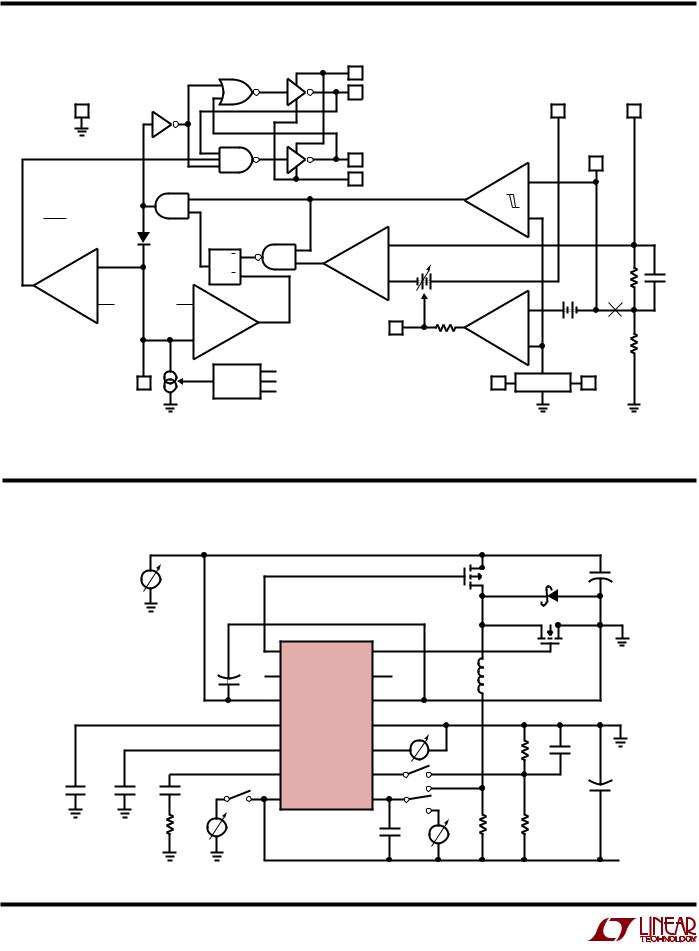
P-DRIVE (Pin 1): High Current Drive for Top P-Channel MOSFET. Voltage swing at this pin is from VIN to ground.
NC (Pin 2): No Connection. Can connect to power ground.
VIN (Pin 3): Main Supply Pin. Must be closely decoupled to power ground Pin 12.
CT (Pin 4): External capacitor CT from Pin 4 to ground sets the operating frequency. The actual frequency is also dependent upon the input voltage.
INTVCC (Pin 5): Internal Supply Voltage, Nominally 3.3V. Can be decoupled to signal ground. Do not externally load this pin.
ITH (Pin 6): Gain Amplifier Decoupling Point. The current comparator threshold increases with the Pin 6 voltage.
SENSE– (Pin 7): Connects to internal resistive divider which sets the output voltage in LTC1148-3.3 and LTC1148-5 versions. Pin 7 is also the (–) input for the current comparator.
SENSE+ (Pin 8): The (+) Input to the Current Comparator. A built-in offset between Pins 7 and 8 in conjunction with RSENSE sets the current trip threshold.
VFB (Pin 9): For the LTC1148 adjustable version, Pin 9 serves as the feedback pin from an external resistive divider used to set the output voltage. On LTC1148-3.3 and LTC1148-5 versions this pin is not used.
SHUTDOWN (Pin 10): When grounded, the LTC1148 series operates normally. Pulling Pin 10 high holds both MOSFETs off and puts the LTC1148 series in micropower shutdown mode. Requires CMOS logic signal with tR, tF < 1μs, should not be left floating.
SGND (Pin 11): Small-Signal Ground. Must be routed separately from other grounds to the (–) terminal of COUT.
PGND (Pin 12): Driver Power Ground. Connects to source of N-channel MOSFET and the (–) terminal of CIN.
NC (Pin 13): No Connection. Can connect to power ground.
N-DRIVE (Pin 14): High Current Drive for Bottom N-Channel MOSFET. Voltage swing at Pin 14 is from ground to VIN.
5
LTC1148
LTC1148-3.3/LTC1148-5
FUUCTIOUAL DIAGRAW Pin 9 connection shown for LTC1148-3.3 and LTC1148-5; changes create LTC1148.
SGND
11
 SLEEP
SLEEP
+ S –
|
|
|
|
3 |
VIN |
|
|
|
|
|
|
|
|
|
|
1 |
P-DRIVE |
|
|
SENSE+ |
|
SENSE– |
|
|
|
|
|
|
|
|
|
|
8 |
|
7 |
|
|
|
|
|
|
|
|
|
ADJUSTABLE |
||
|
|
|
|
|
|
|
|
|
|
VERSION |
|
|
|
|
|
14 |
N-DRIVE |
|
|
|
VFB |
||
|
|
|
|
|
|
|
|
9 |
|||
|
|
|
|
|
|
|
|
|
|
|
|
|
|
|
|
12 |
PGND |
|
|
– |
|
|
|
|
|
|
|
|
|
|
|
|
|
|
|
|
|
|
|
|
|
|
V |
|
|
|
|
|
|
|
|
|
|
|
|
+ |
|
|
|
|
|
R |
|
|
– |
25mV TO 150mV |
|
|
|
|
|
|
|
|
|
C |
|
|
|
|
|||
|
|
Q |
|
|
– |
+ |
|
|
|
|
|
|
|
|
|
|
|
|
|
|
|||
|
|
S |
|
|
+ |
|
|
|
5pF |
||
|
|
|
|
|
|
|
|
VOS |
|
|
|
VTH2 |
VTH1 |
– |
|
|
|
|
|
|
|
|
|
|
|
|
|
13k |
– |
|
|
|
|||
|
|
T |
|
|
|
|
|
|
|
||
|
|
|
|
ITH |
6 |
|
|
|
|
||
|
|
|
|
G |
|
|
|
|
|||
|
|
+ |
|
|
|
|
|
|
|||
|
|
|
|
|
|
|
+ |
1.25V |
|
100k |
|
|
|
OFF-TIME |
VIN |
– |
|
|
|
|
|
|
|
|
4 |
CONTROL |
SENSE |
|
|
|
SHUTDOWN 10 |
REFERENCE |
5 |
INTVCC |
|
|
CT |
|
VFB |
|
|
|
|
|
|
|
|
|
|
|
|
|
|
|
|
|
|
LTC1148 • FD |
|
|
|
|
|
|
|
|
|
|
|
|
|
TEST CIRCUIT
|
+ |
|
|
|
|
|
|
|
|
|
|
|
|
+ |
|
|
VIN |
|
|
|
|
|
|
|
|
IRF9Z34 |
1N5818 |
330μF |
|
|
|
|
|
|
|
|
|
|
|
|
|
|
IRFZ34 |
|
|
|
|
|
1 |
P-DRIVE |
N-DRIVE |
14 |
|
|
|
|
|
|
|
|
|
|
|
|
|
|
|
|
|
|
|
|||
|
|
|
1μF |
2 |
NC |
|
NC |
13 |
|
50μH |
|
|
|
|
|
|
|
|
|
|
|
|
|
|
|
||||
|
|
+ |
|
LTC1148 |
|
|
|
|
|
|
|
|||
|
|
|
3 |
12 |
|
|
|
|
|
|
||||
|
|
|
VIN |
|
PGND |
|
|
|
|
|
|
|||
|
|
|
|
|
|
|
|
|
|
|
|
|
||
|
|
|
|
4 |
CT |
|
SGND |
11 |
|
|
|
|
|
|
|
|
|
|
|
|
|
V10 |
|
|
|
|
|
||
|
|
|
|
5 |
|
|
|
10 |
|
|
|
|
|
|
|
|
|
|
INTVCC |
SHUTDOWN |
+ |
|
|
|
25k |
100pF |
|||
|
|
|
|
|
|
|
|
|
|
|||||
|
|
|
|
6 |
ITH |
|
NC (VFB) |
9 |
|
|
|
|
|
|
|
|
|
|
|
|
|
|
|
|
|
|
440μF |
||
390pF |
10nF |
3300pF |
|
7 |
|
|
|
8 |
|
|
|
|
|
|
|
SENSE |
– |
SENSE+ |
|
|
|
|
|
+ |
|||||
|
|
+ |
|
|
|
|
|
|
|
|
||||
|
|
|
|
|
|
|
|
+ |
V7 |
RSENSE |
75k |
|
||
|
|
1k |
V7 |
|
|
|
|
|
|
|||||
|
|
|
|
|
1000pF |
|
0.05 |
Ω |
|
|||||
|
|
|
|
|
|
|
|
|
TO |
|
|
|
||
|
|
|
|
|
|
|
|
|
|
V8 |
|
|
|
|
|
|
|
|
|
|
|
|
|
|
|
|
|
|
VOUT |
6
 Loading...