


LTC1445IN
Linear Technology LTC1445IN, LTC1445CS, LTC1445CN, LTC1444IS, LTC1444CN Datasheet
...
FEATURES
■
Ultralow Quiescent Current: 8.5µA Max
■
Wide Supply Range
Single: 2V to 11V
Dual: ±1V to ±5.5V
■
Input Voltage Range Includes the Negative Supply
■
Reference Output Drives 0.01µF Capacitor
■
Adjustable Hysteresis (LTC1444/LTC1445)
■
TTL/CMOS Compatible Outputs
■
Propagation Delay: 12µs (Typ) (10mV Overdrive)
■
No Crowbar Current
■
40mA Continuous Source Current
■
Pin Compatible Upgrades for MAX924 (LTC1443)
U
APPLICATIO S
■
Battery-Powered System Monitoring
■
Threshold Detectors
■
Window Comparators
■
Oscillator Circuits
LTC1443/LTC1444/LTC1445
Ultralow Power Quad
Comparators with Reference
U
DESCRIPTIO
The LTC®1443/LTC1444/LTC1445 are ultralow power quad
comparators with a built-in reference. The comparators
feature less than 8.5µA supply current over temperature,
an internal reference (1.182V ±1% for LTC1443 or 1.221V
±1% for LTC1444/LTC1445), programmable hysteresis
(LTC1444/LTC1445) and TTL/CMOS output (LTC1443/
LTC1445) that sinks and sources current (open-drain
output for LTC1444). The reference output can drive a
bypass capacitor of up to 0.01µF without oscillation.
The comparators operate from a single 2V to 11V supply
or a dual ±1V to ±5.5V supply (LTC1443). Comparator
hysteresis is easily programmable using two resistors and
the HYST pin (LTC1444/LTC1445). Each comparator’s
input operates from the negative supply to within 1.3V of
the positive supply. The LTC1443/LTC1445 comparator
output stage can continuously source up to 40mA. By
eliminating the cross-conducting current that normally
happens when the comparator changes logic states, power
supply glitches are eliminated.
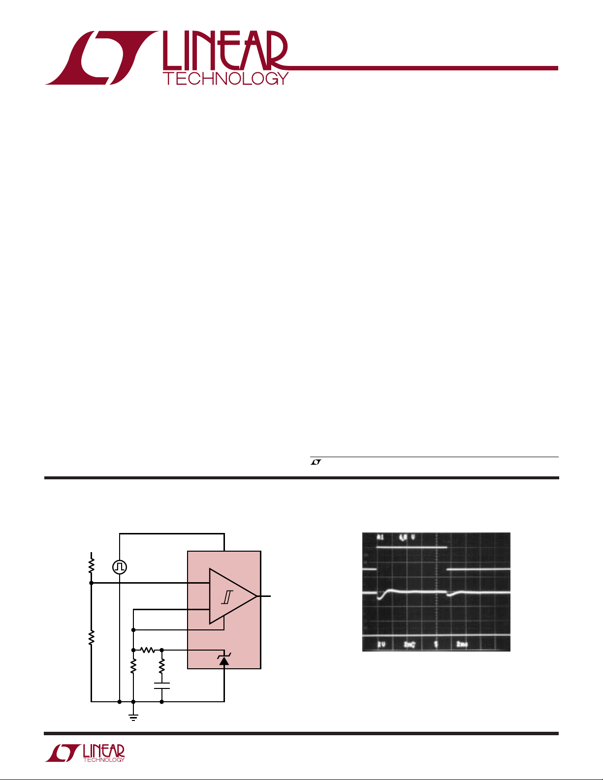
TYPICAL APPLICATIO
Reference Settling Test Circuit
V
IN
3.4M
1%
1.21M
1%
5V
TO 8V
R2
2.4M
R1
10k
5
4
14
8
R3
430Ω
C1
1.0µF
IN A
IN A
HYST
REF
U
+
–
+
–
3
+
V
LTC1445
–
V
9
LTC1443/44/45 • TA01
The LTC1443/LTC1444/LTC1445 are available in the
16-pin SO and PDIP packages.
, LTC and LT are registered trademarks of Linear Technology Corporation.
Reference Settling
8V
+
V
5V
2
OUT
V
REF
2mV/DIV
OUT
2ms/DIV
LTC1443/1444/1445 • TA02
1
LTC1443/LTC1444/LTC1445
WWWU
ABSOLUTE AXI U RATI GS
(Note 1)
Voltage:
V+ to V–, V+ to GND, GND to V–...........12V to –0.3V
IN+, IN–, HYST................. (V+ + 0.3V) to (V– – 0.3V)
REF.................................. (V+ + 0.3V) to (V– – 0.3V)
OUT (LTC1443) ............. (V+ + 0.3V) to (GND – 0.3V)
OUT (LTC1444/LTC1445)
......................................... (V+ + 0.3V) to (V– – 0.3V)
Storage Temperature Range ................. –65°C to 150°C
Lead Temperature Range (Soldering, 10 sec)....... 300°C
UU
W
PACKAGE/ORDER I FOR ATIO
1
OUT B
2
OUT A
+
3
V
–
4
IN A
+
5
IN A
–
6
IN B
+
7
IN B
8
REF
N PACKAGE
16-LEAD PDIP
T
JMAX
T
JMAX
TOP VIEW
16
15
14
13
12
11
10
9
S PACKAGE
16-LEAD PLASTIC SO
= 150°C, θJA = 90°C/W (N)
= 150°C, θJA = 150°C/ W (S)
OUT C
OUT D
GND
IN D
IN D
IN C
IN C
–
V
+
–
+
–
ORDER PART
NUMBER
LTC1443CN
LTC1443CS
LTC1443IN
LTC1443IS
Current:
IN+, IN–, HYST.................................................. 20mA
REF................................................................... 20mA
OUT .................................................................. 50mA
OUT Short Circuit Duration (V+ ≤ 5.5V) ....... Continuous
Power Dissipation.............................................. 500mW
Operating Temperature Range
Commercial ............................................ 0°C to 70°C
Industrial ............................................ – 40°C to 85°C
1
OUT B
2
OUT A
+
3
V
–
4
IN A
+
5
IN A
–
6
IN B
+
7
IN B
8
REF
N PACKAGE
16-LEAD PDIP
T
JMAX
T
JMAX
TOP VIEW
16
15
14
13
12
11
10
9
S PACKAGE
16-LEAD PLASTIC SO
= 150°C, θJA = 90°C/W (N)
= 150°C, θJA = 150°C/ W (S)
OUT C
OUT D
HYST
IN D
IN D
IN C
IN C
–
V
+
–
+
–
ORDER PART
NUMBER
LTC1444CN
LTC1444CS
LTC1444IN
LTC1444IS
LTC1445CN
LTC1445CS
LTC1445IN
LTC1445IS
Consult factory for Military grade parts.
ELECTRICAL CHARACTERISTICS
The ● denotes the specifications which apply over the full operating
temperature range, otherwise specifications are at TA = 25°C. V+ = 5V, V– = GND = 0V, unless otherwise noted.
SYMBOL PARAMETER CONDITIONS MIN TYP MAX UNITS
Power Supply
+
V
I
CC
Comparator
V
OS
I
IN
V
CM
CMRR Common Mode Rejection Ratio V– to (V+ – 1.3V) 0.1 1.0 mV/V
PSRR Power Supply Rejection Ratio V+ = 2V to 11V 0.1 1.0 mV/V
Noise Voltage Noise 100Hz to 100kHz 20 µV
V
HYST
Supply Voltage Range ● 2.0 11.0 V
Supply Current IN+ = IN– = 80mV ● 5.5 8.5 µA
HYST = REF (LTC1444/LTC1445)
Comparator Input Offset Voltage VCM = 2.5V ● ±3.0 ±10.0 mV
+
Input Leakage Current (IN+, IN–)V
–
= V
IN
= 2.5V ● ±0.01 ±1.0 nA
IN
Input Leakage Current (HYST) LTC1444/LTC1445 ● ±0.02 ±1.0 nA
Comparator Input Common Mode Range ● V
–
V+ – 1.3V V
RMS
Hysteresis Input Voltage Range LTC1444, LTC1445 ● REF – 50mV REF V
2
LTC1443/LTC1444/LTC1445
ELECTRICAL CHARACTERISTICS
The ● denotes the specifications which apply over the full operating
temperature range, otherwise specifications are at TA = 25°C. V+ = 5V, V– = GND = 0V, unless otherwise noted.
SYMBOL PARAMETER CONDITIONS MIN TYP MAX UNITS
t
PD
V
OH
V
OL
Propagation Delay Overdrive = 10mV, C
Overdrive = 100mV, C
= 100pF 12 µs
OUT
= 100pF 4 µs
OUT
Output High Voltage IO = –15mA; LTC1443/LTC1445 ● V+ – 0.4V V
Output Low Voltage IO = 1.8mA; LTC1443 ● GND + 0.4V V
IO = 1.8mA; LTC1444/LTC1445 ● V– + 0.4V V
Reference
V
REF
Reference Voltage No Load, LTC1443 C Temp Range ● 1.170 1.182 1.194 V
I Temp Range ● 1.164 1.200 V
No Load, LTC1444/ C Temp Range ● 1.209 1.221 1.233 V
I
SOURCE
I
SINK
LTC1445
Reference Output Source Current ∆V
Reference Output Sink Current ∆V
∆V
≤ 1mV ● 100 200 µA
REF
≤ 2.5mV 10 15 µA
REF
≤ 5mV ● 10 15 µA
REF
I Temp Range
Noise Voltage Noise 100Hz to 100kHz 100 µV
● 1.203 1.239 V
RMS
The ● denotes the specifications which apply over the full operating temperature range, otherwise specifications are at TA = 25°C.
V+ = 3V, V– = GND = 0V, unless otherwise noted.
SYMBOL PARAMETER CONDITIONS MIN TYP MAX UNITS
Power Supply
+
V
I
CC
Comparator
V
OS
I
IN
V
CM
CMRR Common Mode Rejection Ratio V– to (V+ –1.3V) 0.1 1.0 mV/V
PSRR Power Supply Rejection Ratio V+ = 2V to 11V 0.1 1.0 mV/V
Noise Voltage Noise 100Hz to 100kHz 100 µV
V
HYST
t
PD
V
OH
V
OL
Reference
V
REF
I
SOURCE
I
SINK
Noise Noise Voltage 100Hz to 100kHz 100 µV
Note 1: Absolute Maximum Ratings are those values beyond which the life
of the device may be impaired.
Supply Voltage Range ● 2.0 11.0 V
Supply Current IN+ = IN– = 80mV, HYST = REF ● 58 µA
Comparator Input Offset Voltage VCM = 1.5V ● ±3.0 ±10.0 mV
+
Input Leakage Current (IN+, IN–)V
–
= V
IN
= 1.5V ● ±0.01 ±1.0 nA
IN
Input Leakage Current (HYST) LTC1444/LTC1445 ● ±0.02 ±1.0 nA
Comparator Input Common Mode Range ● V
–
V+ – 1.3V V
RMS
Hysteresis Input Voltage Range LTC1444/LTC1445 ● REF – 50mV REF V
Propagation Delay Overdrive = 10mV, C
Overdrive = 100mV, C
= 100pF 14 µs
OUT
= 100pF 5 µs
OUT
Output High Voltage IO = –10mA, LTC1443/LTC1445 ● V+ – 0.4V V
Output Low Voltage IO = 0.8mA; LTC1443 ● GND + 0.4V V
IO = 0.8mA; LTC1444/LTC1445 ● V– + 0.4V V
Reference Voltage No Load, LTC1443 C Temp Range ● 1.170 1.182 1.194 V
I Temp Range ● 1.164 1.200 V
No Load, LTC1444/ C Temp Range ● 1.209 1.221 1.233 V
LTC1445
Reference Output Source Current ∆V
Reference Output Sink Current ∆V
∆V
I Temp Range
≤ 1mV ● 60 120 µA
REF
≤ 2.5mV 10 15 µA
REF
≤ 5mV ● 10 15 µA
REF
● 1.203 1.239 V
RMS
3
LTC1443/LTC1444/LTC1445
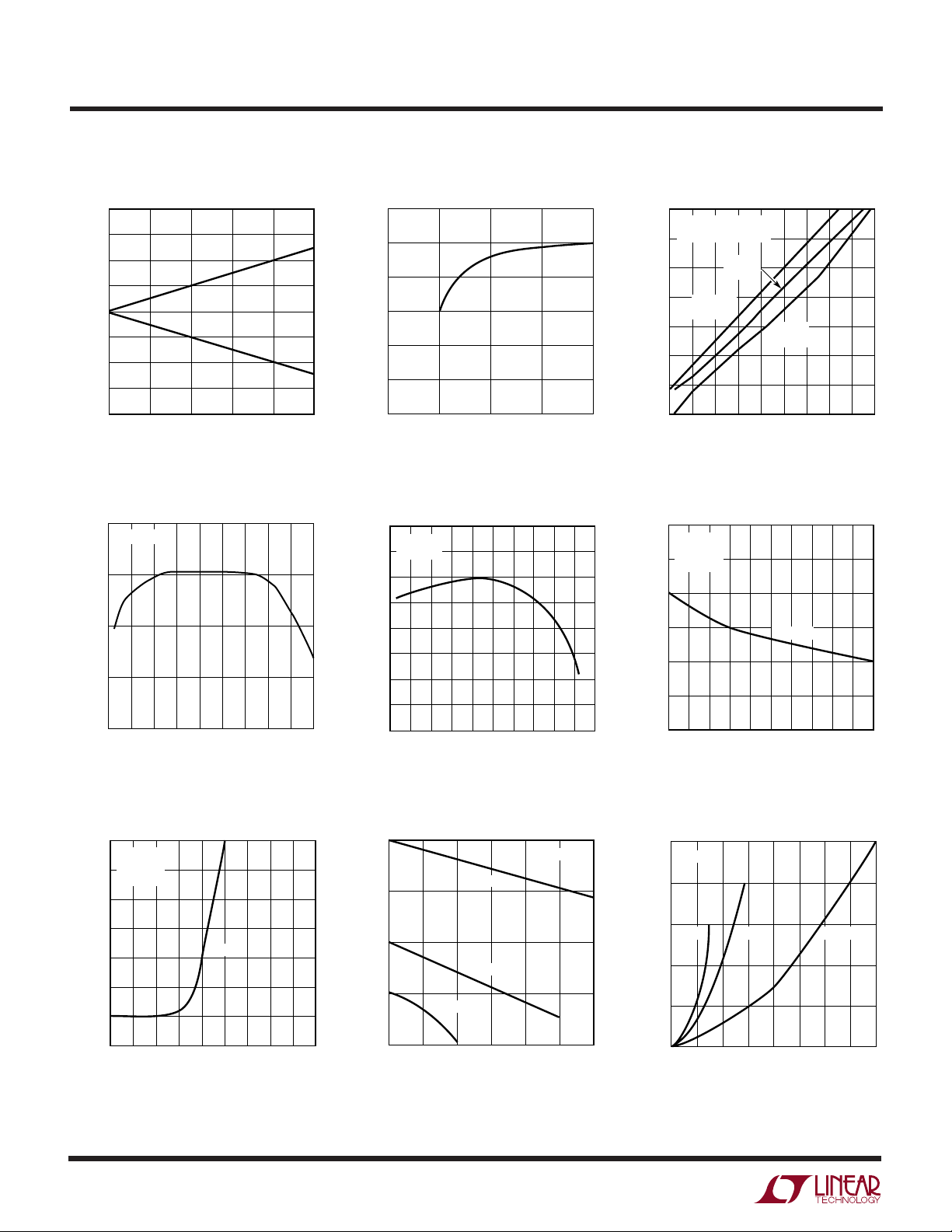
LOAD CURRENT (mA)
REFERENCE VOLTAGE (V)
1.184
1.183
1.182
1.181
1.180
1.179
1.178
0.2 0.4 0.6 0.8
LTC1443/44/45 • TPC06
1.00.10 0.3 0.5 0.7 0.9
V+ = 5V
V
–
= GND
T
A
= 25°C
SOURCE
UW
TYPICAL PERFOR A CE CHARACTERISTICS
LTC1444/LTC1445
Hysteresis Control
80
60
40
20
(mV)
–
0
– IN
+
–20
IN
–40
–60
–80
0
10 20 40
V
REF
– V
HYST
30
(mV)
LTC1443/44/45 • TPC01
50
Supply Current vs Supply Voltage Supply Current vs Temperature
5.2
TA = 25°C
5.0
4.8
4.6
4.4
SUPPLY CURRENT (µA)
4.2
4.0
1.0
1.5 2.0 2.5 3.0
SUPPLY VOLTAGE (V)
LTC1443/44/45 • TPC02
5.8
5.4
5.0
4.6
4.2
3.8
SUPPLY CURRENT (µA)
3.4
3.0
–60
IN+ = (IN– + 100mV)
–
= GND (LTC1443)
V
V+ = 5V
–
= 0V
V
V+ = 5V
–
= –5V
V
–20 60
–40
080100 120
TEMPERATURE (°C)
20
V+ = 3V
–
V
= 0V
40
LTC1443/44/45 • TPC03
LTC1444/LTC1445 Reference
Voltage vs Temperature
1.224
1.220
1.216
1.212
REFERENCE VOLTAGE (V)
1.208
–60
LTC1443 Reference Output
Voltage vs Output Load Current
1.194
1.192
1.190
1.188
1.186
1.184
1.182
REFERENCE OUTPUT VOLTAGE (V)
1.180
0
V+ = 5V
–40 –20 0 20
TEMPERATURE (°C)
V+ = 5V
–
= GND
V
= 25°C
T
A
10 30
15 35 40 45
5
LOAD CURRENT (µA)
40 60 80 100 120
LTC1443/44/45 • TPC04
SINK
20
25
LTC1443/44/45 • TPC07
LTC1443 Reference Voltage
vs Temperature
1.186
V+ = 5V
–60
–
V
–40
= GND
–20
40
0
TEMPERATURE (°C)
60
20
1.184
1.182
1.180
1.178
1.176
1.174
REFERENCE VOLTAGE (V)
1.172
1.170
Comparator Output Voltage High
vs Load Current
5.0
4.0
3.0
2.0
OUTPUT VOLTAGE HIGH (V)
1.0
V+ = 2V
0
10 20 30 40
V+ = 5V
V+ = 3V
LOAD CURRENT (mA)
100
80
120 140
LTC1443/44/45 • TPC05
TA = 25°C
50 60
LTC1443/44/45 • TPC08
LTC1443 Reference Output
Voltage vs Output Load Current
Comparator Output Voltage Low
vs Load Current
2.5
TA = 25°C
2.0
1.5
V+ = 2V V+ = 3V V+ = 5V
1.0
OUTPUT VOLTAGE HIGH (V)
0.5
0
0
10 20
40
30 50 80
LOAD CURRENT (mA)
60 70
LTC1443/44/45 • TPC09
4
 Loading...