


Linear Technology LTC1165CN8, LTC1165, LTC1163CS8, LTC1163CN8, LTC1163 Datasheet
...
FEATURES
■Operates from 1.8V to 6V
■0.01μA Standby Current
■95μA Operating Current per Channel at 3.3V
■Fully Enhances N-Channel Switches
■No External Charge Pump Components
■Built-In Gate Voltage Clamps
■Easily Protected Against Supply Transients
■Controlled Switching ON and OFF Times
■Compatible with 5V, 3V and Sub-3V Logic Families
■Available in 8-Pin SOIC
APPLICATIOUS
■PCMCIA Card 3.3V/5V Switch
■2-Cell High-Side Load Switching
■Boost Regulator Shutdown to Zero Standby Current
■Replacing P-Channel Switches
■Notebook Computer Power Management
■Palmtop Computer Power Management
■Portable Medical Equipment
■Mixed 3.3V and 5V Supply Switching
LTC1163/LTC1165
Triple 1.8V to 6V High-Side MOSFET Drivers
DESCRIPTIOU
The LTC1163/LTC1165 triple low voltage MOSFET drivers make it possible to switch supply or ground referenced loadsthroughinexpensive,lowRDS(ON) N-channelswitches from as little as a 1.8V supply. The LTC1165 has inverting inputs and makes it possible to directly replace P-channel MOSFET switches while maintaining system drive polarity. The LTC1163 has noninverting inputs.
Micropower operation, with 0.01μA standby current and 95μA operating current, coupled with a power supply range of 1.8V to 6V, make the LTC1163/LTC1165 ideally suited for 2- to 4-cell battery-powered applications. The LTC1163/LTC1165 are also well suited for sub-3V, 3.3V and 5V nominal supply applications.
The LTC1163/LTC1165 internal charge pumps boost the gate voltage 8V above a 3.3V rail, fully enhancing inexpensive N-channels for highor low-side switch applications.
The LTC1163/LTC1165 are available in both an 8-pin DIP and an 8-pin SOIC.
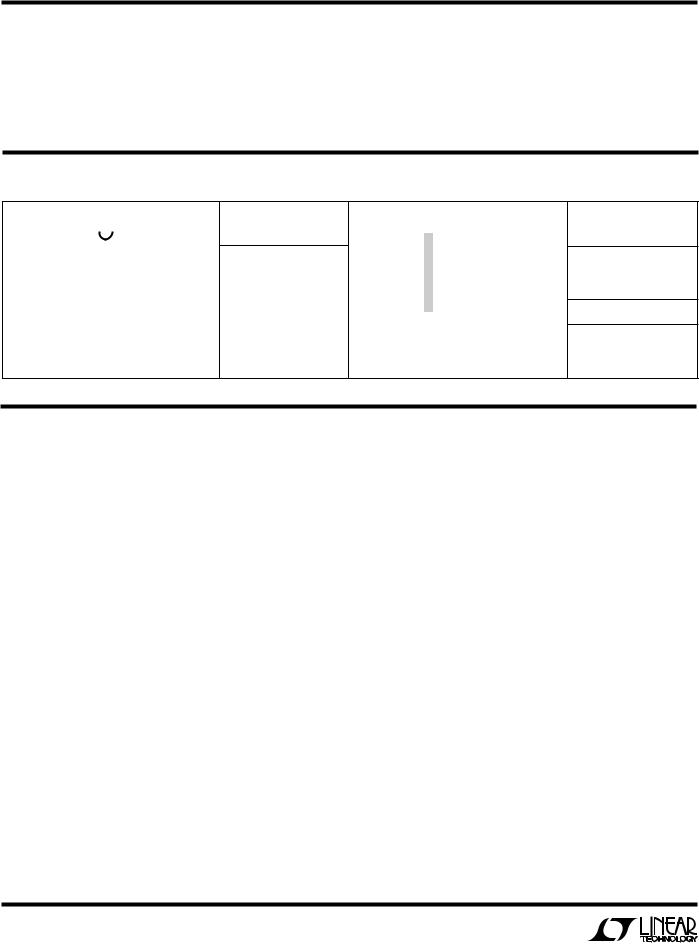
TYPICAL APPLICATIOU
|
2-Cell Triple High-Side Switch |
|
|
|
|
||||
(1.8V TO 3V) |
|
|
|
|
|
|
|
|
|
+ 2-CELL |
+ |
|
|
|
|
|
|
|
|
BATTERY |
10μF |
|
|
|
|
|
|
|
|
PACK |
|
|
|
|
|
|
|
|
(V) |
|
|
|
RFD14N05LSM |
RFD14N05LSM |
RFD14N05LSM |
||||
|
|
|
VOLTAGE |
||||||
CONTROL |
IN1 |
VS |
OUT1 |
|
|
|
|
|
|
|
|
|
|
|
|
||||
IN2 |
LTC1163 OUT2 |
|
|
|
|
|
|
||
LOGIC |
2-CELL |
2-CELL |
2-CELL |
OUTPUTGATE |
|||||
OR μP |
|
LTC1165 |
|
||||||
|
|
|
|
|
|
|
|
||
IN3 |
|
OUT3 |
|
|
|
|
|
|
|
|
GND |
|
|
|
|
|
|
||
|
|
|
|
|
|
|
|
|
|
LTC1163 HAS NONINVERTING INPUTS |
LOAD |
LOAD |
LOAD |
|
|||||
|
|
|
|
|
|
||||
LTC1165 HAS INVERTING INPUTS |
|
|
|
|
|
|
|||
|
|
|
|
|
|
|
LTC1163/65 • TA01 |
|
|
MOSFET Switch Gate Voltage
18
16
14
12
10
8
6
4
2
0
0 |
1 |
2 |
3 |
4 |
5 |
6 |
SUPPLY VOLTAGE (V)
LTC1163/65 • TA02
1
LTC1163/LTC1165
ABSOLUTE WAXIWUW RATIUGS
Supply Voltage ......................................................... |
7V |
Any Input Voltage .......................... |
7V to (GND – 0.3V) |
Any Output Voltage ....................... |
20V to (GND – 0.3V) |
Current (Any Pin)................................................. |
50mA |
Operating Temperature Range |
0°C to 70°C |
LTC1163C/LTC1165C ........................... |
|
Storage Temperature Range ................ |
– 65°C to 150°C |
Lead Temperature (Soldering, 10 sec)................. |
300°C |
PACKAGE/ORDER IUFORWATIOU
|
|
TOP VIEW |
|
|
IN1 |
|
|
|
VS |
|
|
|
||
1 |
|
8 |
||
IN2 |
|
|
|
OUT1 |
2 |
|
7 |
||
IN3 |
|
|
|
OUT2 |
3 |
|
6 |
||
GND |
|
|
|
OUT3 |
4 |
|
5 |
||
|
|
|
|
|
N8 PACKAGE
8-LEAD PLASTIC DIP
TJMAX = 100°C, θJA = 130°C/W
ORDER PART
NUMBER
LTC1163CN8
LTC1165CN8
|
|
|
TOP VIEW |
|
|
IN1 |
|
|
|
|
VS |
1 |
|
|
8 |
||
IN2 |
|
|
|
|
OUT1 |
2 |
|
|
7 |
||
IN3 |
|
|
|
|
OUT2 |
3 |
|
|
6 |
||
GND |
|
|
|
|
OUT3 |
4 |
|
|
5 |
||
|
|
|
|
|
|
S8 PACKAGE
8-LEAD PLASTIC SOIC
TJMAX = 100°C, θJA = 150°C/W
ORDER PART
NUMBER
LTC1163CS8
LTC1165CS8
S8 PART MARKING
1163
1165
ELECTRICAL CHARACTERISTICS VS = 1.8V to 6V, TA = 25°C, unless otherwise noted.
|
|
|
|
LTC1163C/LTC1165C |
|
||
SYMBOL |
PARAMETER |
CONDITIONS |
|
MIN |
TYP |
MAX |
UNITS |
|
|
|
|
|
|
|
|
IQ |
Quiescent Current OFF |
VS = 1.8V, VIN1 = VIN2 = VIN3 = VOFF (Note 1,2) |
|
|
0.01 |
1 |
μA |
|
|
VS = 3.3V, VIN1 = VIN2 = VIN3 = VOFF (Note 1,2) |
|
|
0.01 |
1 |
μA |
|
|
VS = 5V, VIN1 = VIN2 = VIN3 = VOFF (Note 1,2) |
|
|
0.01 |
1 |
μA |
|
Quiescent Current ON |
VS = 1.8V, VIN = VON (Note 2,3) |
|
|
60 |
120 |
μA |
|
|
VS = 3.3V, VIN = VON (Note 2,3) |
|
|
95 |
200 |
μA |
|
|
VS = 5V, VIN = VON (Note 2,3) |
|
|
180 |
400 |
μA |
VINH |
Input High Voltage |
1.8V < VS < 2.7V |
● |
80% × VS |
|
|
V |
|
|
2.7V < VS < 6V |
● |
70% × VS |
|
|
V |
VINL |
Input Low Voltage |
1.8V < VS < 6V |
● |
|
|
15% × VS |
V |
IIN |
Input Current |
0V ≤ VIN ≤ VS |
● |
|
|
±1 |
μA |
CIN |
Input Capacitance |
|
|
|
5 |
|
pF |
VGATE – VS |
Gate Voltage Above Supply |
VS = 1.8V, VIN = VON (Note 2) |
● |
3.5 |
4.1 |
6.0 |
V |
|
|
VS = 2V, VIN = VON (Note 2) |
● |
4.0 |
4.6 |
7.0 |
V |
|
|
VS = 2.2V, VIN = VON (Note 2) |
● |
4.5 |
5.2 |
8.0 |
V |
|
|
VS = 3.3V, VIN = VON (Note 2) |
● |
6.0 |
8.0 |
9.5 |
V |
|
|
VS = 5V, VIN = VON (Note 2) |
● |
5.0 |
9.0 |
13.0 |
V |
tON |
Turn-ON Time |
VS = 3.3V, CGATE = 1000pF |
|
|
|
|
μs |
|
|
Time for VGATE > VS + 1V |
|
40 |
120 |
400 |
|
|
|
Time for VGATE > VS + 2V |
|
60 |
180 |
600 |
μs |
|
|
VS = 5V, CGATE = 1000pF |
|
|
|
|
μs |
|
|
Time for VGATE > VS + 1V |
|
30 |
95 |
300 |
|
|
|
Time for VGATE > VS + 2V |
|
40 |
130 |
400 |
μs |
2
LTC1163/LTC1165
ELECTRICAL CHARACTERISTICS VS = 1.8V to 6V, TA = 25°C, unless otherwise noted.
|
|
|
|
|
LTC1163C/LTC1165C |
|
||
SYMBOL |
PARAMETER |
CONDITIONS |
|
|
MIN |
TYP |
MAX |
UNITS |
|
|
|
|
|
|
|
|
|
tOFF |
Turn-OFF Time |
VS = 3.3V, CGATE = 1000pF |
|
|
|
|
|
μs |
|
|
Time for VGATE < 0.5V |
|
|
20 |
65 |
200 |
|
|
|
VS = 5V, CGATE = 1000pF |
|
|
|
|
|
μs |
|
|
Time for VGATE < 0.5V |
|
|
15 |
45 |
150 |
|
The ● denotes specifications which apply over the full operating |
Note 2: LTC1163: VOFF = 0V, VON = VS. LTC1165: VOFF = VS, VON = 0V |
|||||||
temperature range. |
|
Note 3: Quiescent current ON is per driver and is measured independently. |
||||||
Note 1: Quiescent current OFF is for all channels in OFF condition.
TYPICAL PERFORWAUCE CHARACTERISTICS
Standby Supply Current
|
5 |
|
|
|
|
|
|
|
|
|
|
|
|
|
|
|
|
|
|
TA = |
25°C |
|
|
|
|
|
|
|
|
|
|
|
4 |
|
|
ALL THREE INPUTS = OFF |
|
|
|
|
|
|
|
||||
(μA) |
|
|
|
|
|
|
|
|
|
|
|
|
|
|
|
3 |
|
|
|
|
|
|
|
|
|
|
|
|
|
|
|
CURRENT |
|
|
|
|
|
|
|
|
|
|
|
|
|
|
|
2 |
|
|
|
|
|
|
|
|
|
|
|
|
|
|
|
SUPPLY |
|
|
|
|
|
|
|
|
|
|
|
|
|
|
|
1 |
|
|
|
|
|
|
|
|
|
|
|
|
|
|
|
|
|
|
|
|
|
|
|
|
|
|
|
|
|
|
|
|
0 |
|
|
|
|
|
|
|
|
|
|
|
|
|
|
|
|
|
|
|
|
|
|
|
|
|
|
|
|
|
|
|
–1 |
|
|
|
|
|
|
|
|
|
|
|
|
|
|
|
|
|
1 |
2 |
3 |
|
4 |
5 |
6 |
||||||
|
0 |
|
|||||||||||||
|
|
|
|
|
|
SUPPLY VOLTAGE (V) |
|
|
|
|
|||||
|
|
|
|
|
|
|
|
|
|
|
|
LTC1163/65 • TPC01 |
|||
|
|
Input Threshold Voltage |
|
|
|
|
|||||||||
|
6 |
|
|
|
|
|
|
|
|
|
|
|
|
|
|
|
|
|
|
|
|
|
|
|
|
|
|
|
|
|
|
|
|
|
|
TA = |
25°C |
|
|
|
|
|
|
|
|
|
|
(V) |
5 |
|
|
|
|
|
|
|
|
|
|
|
|
|
|
|
|
|
|
|
|
|
|
|
|
|
|
|
|
||
VOLTAGE |
4 |
|
|
|
|
|
|
|
|
|
|
|
|
|
|
THRESHOLD |
2 |
|
|
|
|
|
|
|
|
|
|
|
|
|
|
|
3 |
|
|
|
|
|
|
VHI |
|
|
|
|
|
|
|
|
|
|
|
|
|
|
|
|
|
|
|
|
|
||
INPUT |
|
|
|
|
|
|
|
|
|
|
VLO |
|
|
|
|
1 |
|
|
|
|
|
|
|
|
|
|
|
|
|
|
|
|
|
|
|
|
|
|
|
|
|
|
|
|
|
||
|
0 |
|
|
|
|
|
|
|
|
|
|
|
|
|
|
|
|
|
1 |
2 |
3 |
|
4 |
5 |
6 |
||||||
|
0 |
|
|||||||||||||
SUPPLY VOLTAGE (V)
LTC1163/65 • TPC04
Supply Current per Driver ON
|
600 |
|
|
|
|
|
|
|
|
|
|
|
|
|
|
|
|
|
|
|
|
|
|
|
|
|
|
|
|
|
|
|
|
|
|
|
|
|
|
|
|
TA = |
25°C |
|
|
|
|
|
|
|
|
|
|
|
|
|
|
500 |
|
|
ONE INPUT = ON |
|
|
|
|
|
|
|
|
|
|
||||
|
|
|
OTHER INPUTS = OFF |
|
|
|
|
|
|
|
|
|||||||
|
|
|
|
|
|
|
|
|
|
|
|
|||||||
(μA) |
400 |
|
|
|
|
|
|
|
|
|
|
|
|
|
|
|
|
|
CURRENT |
|
|
|
|
|
|
|
|
|
|
|
|
|
|
|
|
|
|
300 |
|
|
|
|
|
|
|
|
|
|
|
|
|
|
|
|
|
|
SUPPLY |
|
|
|
|
|
|
|
|
|
|
|
|
|
|
|
|
|
|
200 |
|
|
|
|
|
|
|
|
|
|
|
|
|
|
|
|
|
|
|
|
|
|
|
|
|
|
|
|
|
|
|
|
|
|
|
|
|
|
100 |
|
|
|
|
|
|
|
|
|
|
|
|
|
|
|
|
|
|
|
|
|
|
|
|
|
|
|
|
|
|
|
|
|
|
|
|
|
0 |
|
|
|
|
|
|
|
|
|
|
|
|
|
|
|
|
|
|
|
|
1 |
2 |
|
3 |
4 |
5 |
6 |
|||||||||
|
0 |
|
|
|||||||||||||||
|
|
|
|
|
|
SUPPLY VOLTAGE (V) |
|
|
|
|
|
|||||||
|
|
|
|
|
|
|
|
|
|
|
|
|
LTC1163/65 • TPC02 |
|||||
|
Turn-ON Time |
|
|
|
|
|
|
|
|
|
|
|||||||
|
600 |
|
|
|
|
|
|
|
|
|
|
|
|
|
|
|
|
|
|
|
|
|
|
|
|
|
|
|
|
|
|
|
|
|
|
|
|
|
|
|
|
CGATE = 1000pF |
|
|
|
|
|
|
|
|
|
|
|
|
||
(μs) |
500 |
|
|
|
|
|
|
|
|
|
|
|
|
|
|
|
|
|
|
|
|
|
|
|
|
|
|
|
|
|
|
|
|
|
|
||
400 |
|
|
|
|
|
|
|
|
|
|
|
|
|
|
|
|
|
|
|
|
|
|
|
|
|
|
|
|
|
|
|
|
|
|
|
||
TIME |
300 |
|
|
|
|
|
|
|
|
|
|
|
|
|
|
|
|
|
TURN-ON |
|
|
|
|
|
|
|
|
|
|
|
|
|
|
|
|
|
|
200 |
|
|
|
|
|
|
|
|
|
|
|
|
|
|
|
|
|
|
|
|
|
|
|
|
|
|
|
|
VGS = 2V |
|
|
|
|
|
|||
|
|
|
|
|
|
|
|
|
|
|
|
|
|
|
||||
|
100 |
|
|
|
|
|
|
|
|
|
|
|
|
|
|
|
|
|
|
|
|
|
|
|
|
|
|
|
|
VGS = 1V |
|
|
|
|
|
||
|
|
|
|
|
|
|
|
|
|
|
|
|
|
|
|
|
||
|
0 |
|
|
|
|
|
|
|
|
|
|
|
|
|
|
|
|
|
|
|
|
1 |
2 |
|
3 |
4 |
5 |
6 |
|||||||||
|
0 |
|
|
|||||||||||||||
SUPPLY VOLTAGE (V)
LTC1163/65 • TPC05
Gate Voltage Above Supply
|
12 |
|
|
|
|
|
|
|
|
|
|
|
|
|
|
|
|
|
|
|
|
|
TA = |
25°C |
|
|
|
|
|
|
10 |
|
|
|
|
|
|
|
|
|
|
|
|
|
|
|
|
|
|
(V) |
8 |
|
|
|
|
|
|
|
|
|
|
|
|
|
|
|
|
||
|
|
|
|
|
|
|
|
|
|
S |
|
|
|
|
|
|
|
|
|
– V |
6 |
|
|
|
|
|
|
|
|
|
|
|
|
|
|
|
|
||
GATE |
|
|
|
|
|
|
|
|
|
|
|
|
|
|
|
|
|
|
|
V |
4 |
|
|
|
|
|
|
|
|
|
|
|
|
|
|
|
|
|
|
|
2 |
|
|
|
|
|
|
|
|
|
|
|
|
|
|
|
|
|
|
|
0 |
|
|
|
|
|
|
|
|
|
|
|
|
|
|
|
|
|
0 1 2 3 4 5 6 SUPPLY VOLTAGE (V)
LTC1163/65 • TPC03
Turn-OFF Time
|
300 |
|
|
|
|
|
|
|
|
|
|
|
|
|
|
|
CGATE |
= 1000pF |
|
|
|
|
|
|
|
|
|
|
250 |
|
TIME FOR VGATE < 0.5V |
|
|
|
|
|
|||||
(μs) |
200 |
|
|
|
|
|
|
|
|
|
|
|
|
|
|
|
|
|
|
|
|
|
|
|
|
||
TIME |
150 |
|
|
|
|
|
|
|
|
|
|
|
|
-OFF |
|
|
|
|
|
|
|
|
|
|
|
|
|
|
|
|
|
|
|
|
|
|
|
|
|
||
|
|
|
|
|
|
|
|
|
|
|
|
|
|
TURN |
100 |
|
|
|
|
|
|
|
|
|
|
|
|
|
|
|
|
|
|
|
|
|
|
|
|
|
|
|
50 |
|
|
|
|
|
|
|
|
|
|
|
|
|
|
|
|
|
|
|
|
|
|
|
|
|
|
|
0 |
|
|
|
|
|
|
|
|
|
|
|
|
|
|
1 |
2 |
3 |
4 |
5 |
6 |
||||||
|
0 |
||||||||||||
SUPPLY VOLTAGE (V)
LTC1163/65 • TA06
3
 Loading...